DATA SHEET
Product specification
Supersedes data of 1997 Apr 14
File under Discrete Semiconductors, SC16
1998 Mar 12
DISCRETE SEMICONDUCTORS
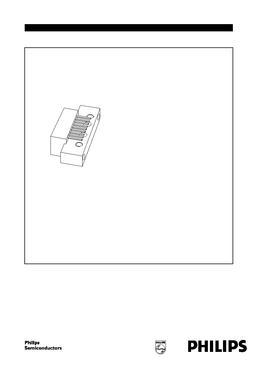
BGD885
CATV amplifier module
book, halfpage
M3D248
1998 Mar 12
2
Philips Semiconductors
Product specification
CATV amplifier module
BGD885
FEATURES
∑
Excellent linearity
∑
Extremely low noise
∑
Silicon nitride passivation
∑
Rugged construction
∑
Gold metallization ensures excellent reliability.
DESCRIPTION
Hybrid amplifier module for CATV/MATV systems
operating over a frequency range of 40 to 860 MHz at a
voltage supply of 24 V (DC).
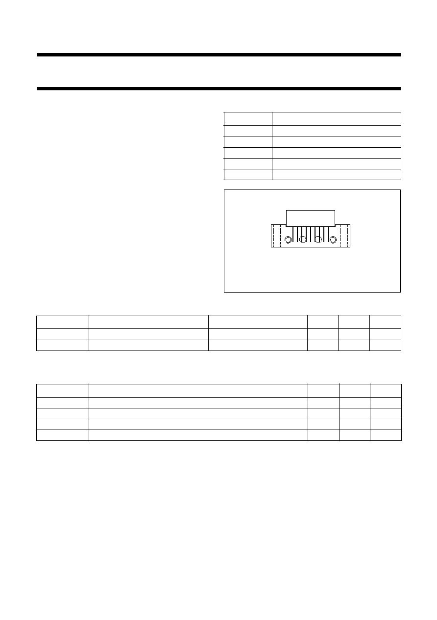
PINNING - SOT115D
PIN
DESCRIPTION
1
input
2, 3, 5, 6, 7
common
4
10 V, 200 mA supply terminal
8
+V
B
9
output
Fig.1 Simplified outline.
handbook, halfpage
7
8
9
2
4
6
3
5
1
Side view
MBK049
QUICK REFERENCE DATA
LIMITING VALUES
In accordance with the Absolute Maximum Rating System (IEC 134).
SYMBOL
PARAMETER
CONDITIONS
MIN.
MAX.
UNIT
G
p
power gain
f = 50 MHz
16.5
17.5
dB
I
tot
total current consumption (DC)
V
B
= 24 V
-
450
mA
SYMBOL
PARAMETER
MIN.
MAX.
UNIT
V
B
DC supply voltage
-
26
V
V
i
RF input voltage
-
65
dBmV
T
stg
storage temperature
-
40
+100
∞
C
T
mb
operating mounting base temperature
-
20
+100
∞
C
1998 Mar 12
3
Philips Semiconductors
Product specification
CATV amplifier module
BGD885
CHARACTERISTICS
Table 1
Bandwidth 40 to 860 MHz; V
B
= 24 V; T
mb
= 35
∞
C; Z
S
= Z
L
= 75
Notes
1. Decrease per octave of 1.5 dB.
2. V
p
= 59 dBmV at f
p
= 349.25 MHz;
V
q
= 59 dBmV at f
q
= 403.25 MHz;
measured at f
p
+ f
q
= 752.5 MHz.
3. Measured according to DIN45004B:
f
p
= 341.25 MHz; V
p
= V
o
;
f
q
= 348.25 MHz; V
q
= V
o
-
6 dB;
f
r
= 350.25 MHz; V
r
= V
o
-
6 dB;
measured at f
p
+ f
q
-
f
r
= 339.25 MHz.
4. Measured according to DIN45004B:
f
p
= 851.25 MHz; V
p
= V
o
;
f
q
= 858.25 MHz; V
q
= V
o
-
6 dB;
f
r
= 860.25 MHz; V
r
= V
o
-
6 dB;
measured at f
p
+ f
q
-
f
r
= 849.25 MHz.
5. The module normally operates at V
B
= 24 V, but is able to withstand supply transients up to 30 V.
SYMBOL
PARAMETER
CONDITIONS
MIN.
MAX.
UNIT
G
p
power gain
f = 50 MHz
16.5
17.5
dB
SL
slope cable equivalent
f = 40 to 860 MHz
0.2
1.6
dB
FL
flatness of frequency response
f = 40 to 860 MHz
-
±
0.5
dB
S
11
input return losses
f = 40 MHz; note 1
20
-
dB
f = 800 to 860 MHz
10
-
dB
S
22
output return losses
f = 40 MHz; note 1
20
-
dB
f = 800 to 860 MHz
10
-
dB
d
2
second order distortion
note 2
-
-
53
dB
V
o
output voltage
d
im
=
-
60 dB; note 3
64
-
dBmV
d
im
=
-
60 dB; note 4
63
-
dBmV
F
noise figure
f = 50 MHz
-
8
dB
f = 550 MHz
-
8
dB
f = 650 MHz
-
8
dB
f = 750 MHz
-
8
dB
f = 860 MHz
-
8
dB
I
tot
total current consumption (DC)
note 5
-
450
mA
1998 Mar 12
4
Philips Semiconductors
Product specification
CATV amplifier module
BGD885
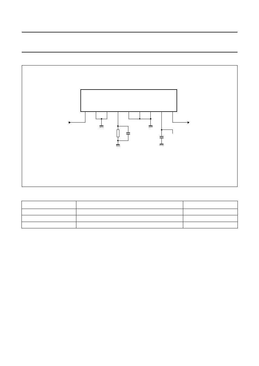
1
2
3
4
5
6
7
8
9
BGD885
input
C2
output
VB = 24 V
MEA094-2
10 V
C1
Fig.2 Test circuit.
List of components (see Fig.2)
COMPONENT
DESCRIPTION
VALUE
C1
ceramic multilayer capacitor
1 nF (max.)
C2
ceramic multilayer capacitor
1 nF
R
resistor
56
,
2 W
1998 Mar 12
5
Philips Semiconductors
Product specification
CATV amplifier module
BGD885
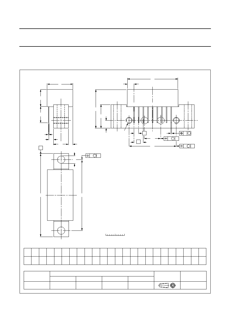
PACKAGE OUTLINE
UNIT
A2
max.
c
e
e1
q
Q
max.
q1
U1
max.
U2
W
REFERENCES
OUTLINE
VERSION
EUROPEAN
PROJECTION
ISSUE DATE
IEC
JEDEC
EIAJ
mm
20.8
9.1
0.51
0.38
0.25 27.2 2.54 13.75 2.54 5.08 12.7
8.8
4.15
3.85
2.4
38.1 25.4
q2
10.2
4.2 44.75
8
0.25
0.1
3.8
b
F
P
6-32
UNC
y
w
S
DIMENSIONS (mm are the original dimensions)
SOT115D
0
5
10 mm
scale
A
max.
D
max.
L
min.
E
max.
Z
max.
Rectangular single-ended package; aluminium flange; 2 vertical mounting holes;
2 x 6-32 UNC and 2 extra horizontal mounting holes; 9 gold-plated in-line leads
SOT115D
D
U1
q
q1
b
F
S
A
Z
E
A2
L
c
d
Q
U2
M
w
7
8
9
2
3
W
e
e1
5
6
4
P
y
M
B
y
M
B
1
B
d
max.
97-04-10
q2
y
M
B