 | –≠–ª–µ–∫—Ç—Ä–æ–Ω–Ω—ã–π –∫–æ–º–ø–æ–Ω–µ–Ω—Ç: N74F07N | –°–∫–∞—á–∞—Ç—å:  PDF PDF  ZIP ZIP |
Document Outline
- FEATURES
- ORDERING INFORMATION
- PIN CONFIGURATIONS
- LOGIC SYMBOLS
- IEC/IEEE SYMBOLS
- LOGIC DIAGRAMS
- INPUT AND OUTPUT LOADING AND FAN OUT TABLE
- FUNCTION TABLE
- ABSOLUTE MAXIMUM RATINGS
- RECOMMENDED OPERATING CONDITIONS
- DC ELECTRICAL CHARACTERISTICS
- AC ELECTRICAL CHARACTERISTICS
- TYPICAL PROPAGATION DELAYS VERSUS LOAD FOR OPEN COLLECTOR OUTPUTS
- AC WAVEFORMS
- TEST CIRCUIT AND WAVEFORMS
- PACKAGE OUTLINE
- REVISION HISTORY
- Data sheet status
- Definitions
- Disclaimers
Philips
Semiconductors
74F07
Inverter/buffer drivers
Product data
Supersedes data of 1992 Jul 24
2004 Mar 12
INTEGRATED CIRCUITS

Philips Semiconductors
Product data
74F07
Hex inverter/buffer drivers (open-collector)
2
2004 Mar 12
FEATURES
∑
Open Collector output drive 64mA
∑
High speed
∑
12V output termination voltage
TYPE
TYPICAL
PROPAGATION
DELAY
TYPICAL SUPPLY
CURRENT
(TOTAL)
74F07
4.5ns
32mA
ORDERING INFORMATION
DESCRIPTION
TYPE NUMBER
PKG DWG #
14-pin plastic small outline package
N74F07D
SOT108≠1
14-pin plastic dual in-line package
N74F07N
SOT27≠1
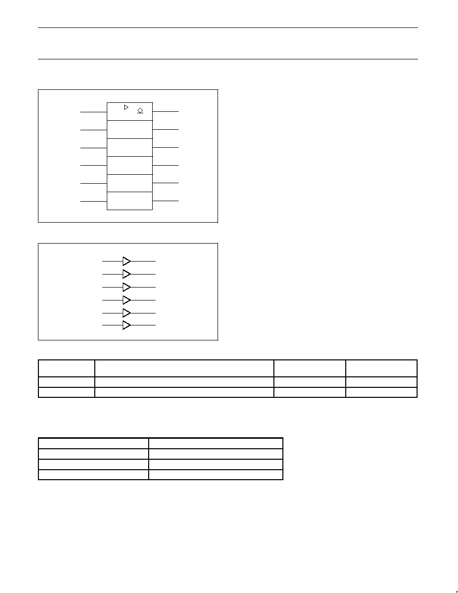
PIN CONFIGURATIONS
14
13
12
11
10
9
8
7
6
5
4
3
2
1
GND
V
CC
Y4
A3
Y3
A4
A5
Y5
A0
Y0
Y2
A1
Y1
A2
SF00017
74F07
LOGIC SYMBOLS
4
6
8
10
1
3
5
9
11 13
V
CC
= Pin 14
GND = Pin 7
SF00019
A0
A1 A2
A3 A4 A5
2
Y0
Y1 Y2
Y3
Y4 Y5
12
74F07
Philips Semiconductors
Product data
74F07
Hex inverter/buffer drivers (open-collector)
2004 Mar 12
3
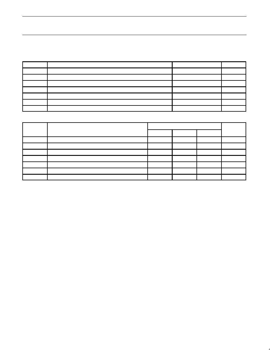
IEC/IEEE SYMBOLS
13
SF00021
12
11
10
9
8
5
6
3
4
1
2
74F07
LOGIC DIAGRAMS
V
CC
= Pin 14
GND = Pin 7
SF00023
2
4
6
8
10
12
Y0
Y1
Y2
Y3
Y4
Y5
1
3
5
9
11
13
A0
A1
A2
A3
A4
A5
74F07
INPUT AND OUTPUT LOADING AND FAN OUT TABLE
PINS
DESCRIPTION
74F (U.L.)
HIGH/LOW
LOAD VALUE
HIGH/LOW
An
Data inputs
1.0/1.0
20
µ
A/0.6mA
Yn
Data outputs
OC/106.7
OC/64mA
NOTES:
1. One (1.0) FAST unit load is defined as: 20
µ
A in the High state and 0.6mA in the Low state.
2. OC = Open Collector
FUNCTION TABLE
INPUTS
OUTPUTS
An
Yn
L
L
H
H
NOTES:
1. H = High voltage level
2. L = Low voltage level
Philips Semiconductors
Product data
74F07
Hex inverter/buffer drivers (open-collector)
2004 Mar 12
4
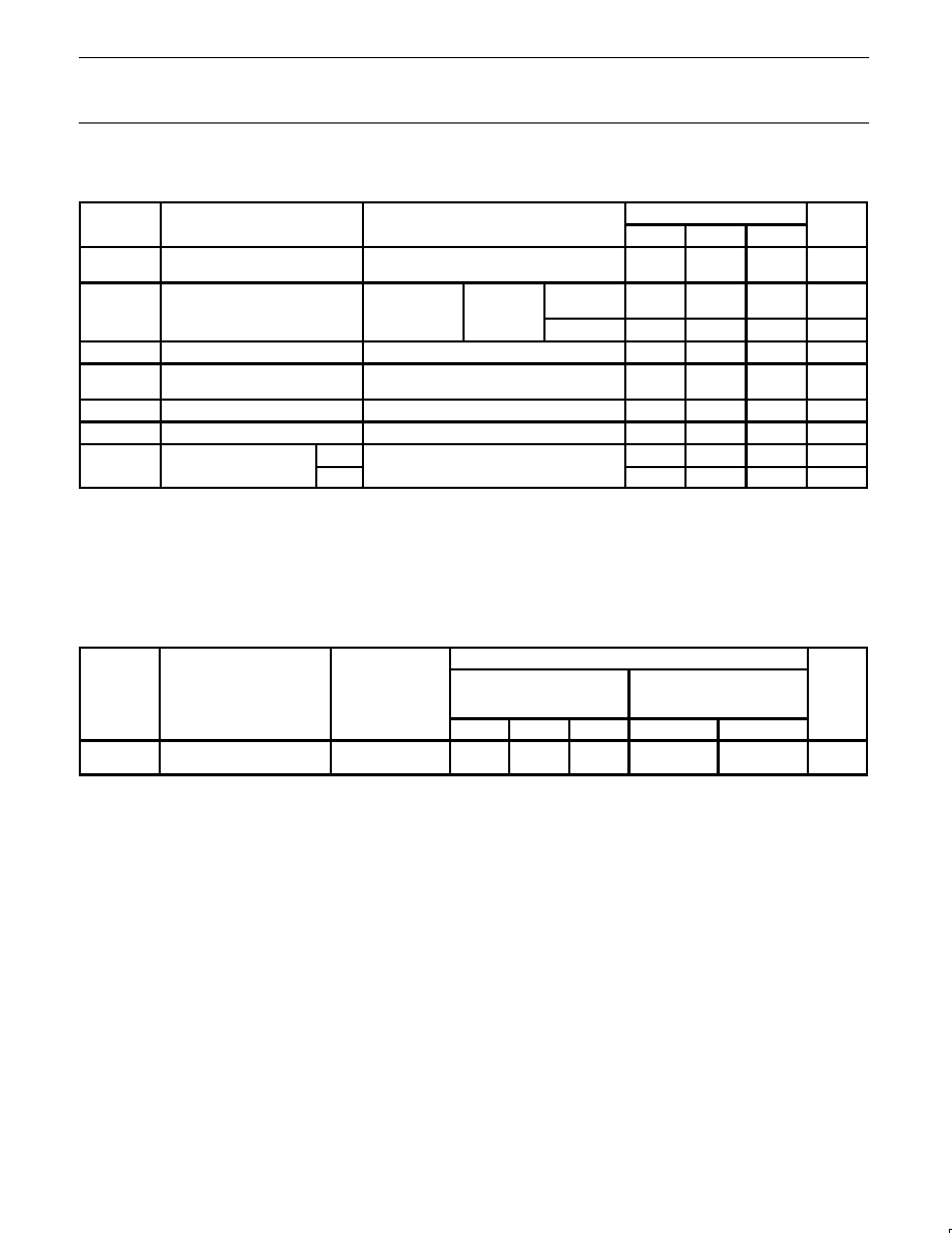
ABSOLUTE MAXIMUM RATINGS
(Operation beyond the limit set forth in this table may impair the useful life of the device.
Unless otherwise noted these limits are over the operating free air temperature range.)
SYMBOL
PARAMETER
RATING
UNIT
V
CC
Supply voltage
≠0.5 to +7.0
V
V
IN
Input voltage
≠0.5 to +7.0
V
I
IN
Input current
≠30 to +5
mA
V
OUT
Voltage applied to output in High output state
≠0.5 to 12
V
I
OUT
Current applied to output in Low output state
128
mA
T
amb
Operating free air temperature range
0 to +70
∞
C
T
stg
Storage temperature range
≠65 to +150
∞
C
RECOMMENDED OPERATING CONDITIONS
SYMBOL
PARAMETER
LIMITS
UNIT
MIN
NOM
MAX
V
CC
Supply voltage
4.5
5.0
5.5
V
V
IH
High-level input voltage
2.0
V
V
IL
Low-level input voltage
0.8
V
I
Ik
Input clamp current
≠18
mA
V
OH
High-level output voltage
12
V
I
OL
Low-level output current
64
mA
T
amb
Operating free air temperature range
0
+70
∞
C
Philips Semiconductors
Product data
74F07
Hex inverter/buffer drivers (open-collector)
2004 Mar 12
5
DC ELECTRICAL CHARACTERISTICS
(Over recommended operating free-air temperature range unless otherwise noted.)
SYMBOL
PARAMETER
TEST CONDITIONS
1
LIMITS
UNIT
MIN
TYP
2
MAX
I
OH
High-level output current
V
CC
= MIN, V
IL
= MAX,
V
OH
= MAX, V
IH
= MIN
250
µ
A
V
OL
Low-level output voltage
V
CC
= MIN,
V
IL
= MAX,
I
OL
= MAX
±
10% V
CC
0.30
0.50
V
V
IH
= MIN
±
5% V
CC
0.30
0.50
V
V
IK
Input clamp voltage
V
CC
= MIN, I
I
= I
IK
≠0.73
≠1.2
V
I
I
Input current at maximum input
voltage
V
CC
= MAX, V
I
= 7.0V
100
µ
A
I
IH
High-level input current
V
CC
= MAX, V
I
= 2.7V
20
µ
A
I
IL
Low-level input current
V
CC
= MAX, V
I
= 0.5V
≠0.6
mA
I
CC
Supply current (total)
I
CCH
V
CC
= MAX
10
14
mA
I
CCL
32
45
mA
NOTES:
1. For conditions shown as MIN or MAX, use the appropriate value specified under recommended operating conditions for the applicable type.
2. All typical values are at V
CC
= 5V, T
amb
= 25
∞
C.
3. Not more than one output should be shorted at a time. For testing I
OS
, the use of high-speed test apparatus and/or sample-and-hold
techniques are preferable in order to minimize internal heating and more accurately reflect operational values. Otherwise, prolonged shorting
of a High output may raise the chip temperature well above normal and thereby cause invalid readings in other parameter tests. In any
sequence of parameter tests, I
OS
tests should be performed last.
AC ELECTRICAL CHARACTERISTICS
LIMITS
SYMBOL
PARAMETER
TEST CONDITION
V
CC
= +5.0V
T
amb
= +25
∞
C
C
L
= 50pF, R
L
= 100
V
CC
= +5.0V
±
10%
T
amb
= 0
∞
C to +70
∞
C
C
L
= 50pF, R
L
= 100
UNIT
Min
Typ
Max
Min
Max
t
PLH
t
PHL
Propagation delay
An to Yn
Waveform 1
2.0
3.0
4.0
5.0
6.0
7.0
2.0
2.5
6.5
7.5
ns