 | –≠–ª–µ–∫—Ç—Ä–æ–Ω–Ω—ã–π –∫–æ–º–ø–æ–Ω–µ–Ω—Ç: N74F139N | –°–∫–∞—á–∞—Ç—å:  PDF PDF  ZIP ZIP |

Philips
Semiconductors
74F139
Dual 1-of-4 decoder/demultiplexer
Product specification
IC15 Data Handbook
1990 Feb 23
INTEGRATED CIRCUITS

Philips Semiconductors
Product specification
74F139
1-of-4 decoder/demultiplexer
2
February 23, 1990
853≠0344 98903
FEATURES
∑
Demultiplexing capability
∑
Two independent 1-of-4 decoders
∑
Multifunction capability
DESCRIPTION
The 74F139 is a high speed, dual 1-of-4 decoder/demultiplexer. This
device has two independent decoders, each accepting two binary
weighted inputs (A0n, A1n) and providing four mutually exclusive
active-Low outputs (Q0n≠Q3n). Each decoder has an active-Low
Enable (E). When E is High, every output is forced High. The Enable
can be used as the Data input for a 1-of-4 demultiplexer application.
TYPE
TYPICAL
PROPAGATION
DELAY
TYPICAL
SUPPLY CURRENT
(TOTAL)
74F139
5.3ns
13mA
PIN CONFIGURATION
16
15
14
13
12
11
10
7
6
5
4
3
2
1
Q3a
V
CC
Q0b
Q1b
Q2b
A1b
Eb
A0b
Ea
A0a
Q2a
A1a
Q0a
Q1a
9
8
GND
Q3b
SF00129
ORDERING INFORMATION
DESCRIPTION
COMMERCIAL RANGE
V
CC
= 5V
±
10%,
T
amb
= 0
∞
C to +70
∞
C
PKG DWG #
16-pin plastic DIP
N74F139N
SOT38-4
16-pin plastic SO
N74F139D
SOT109-1
INPUT AND OUTPUT LOADING AND FAN-OUT TABLE
PINS
DESCRIPTION
74F (U.L.) HIGH/LOW
LOAD VALUE HIGH/LOW
Ana, Anb
Address inputs
1.0/1.0
20
µ
A/0.6mA
Ea, Eb
Enable inputs (active Low)
1.0/1.0
20
µ
A/0.6mA
Q0n≠Q3n
Data outputs (active Low)
50/33
1.0mA/20mA
NOTE: One (1.0) FAST unit load is defined as: 20
µ
A in the High state and 0.6mA in the Low state.
LOGIC SYMBOL
A0a
A1a
Ea
1
2
3
V
CC
= Pin 16
GND = Pin 8
SF00130
Q0a
Q1a Q2a
4
5
6
Q3a
7
A0b
A1b
Eb
15
14
13
Q0b
Q1b Q2b
12
11
10
Q3b
9
DECODER a
DECODER b
IEC/IEEE SYMBOL
SF00131
DEMUX
2
3
1
14
13
15
4
5
6
7
12
11
10
9
0
1
0
1
2
G
0
3
3
Philips Semiconductors
Product specification
74F139
1-of-4 decoder/demultiplexer
February 23, 1990
3
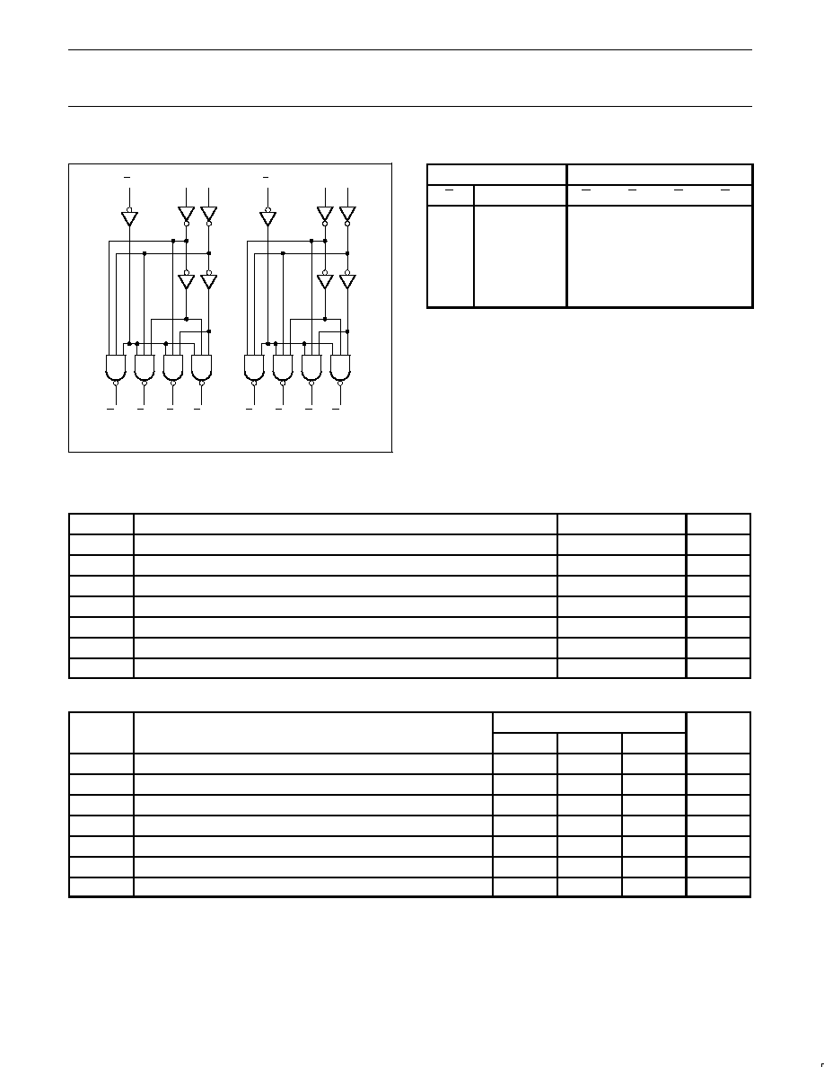
LOGIC DIAGRAM
SF00132
1
2
3
Ea
A0a
A1a
4
5
6
7
Q0a
Q1a
Q2a
Q3a
V
CC
= Pin 16
GND = Pin 8
15
14
13
Eb
A0b
A1b
12
11
10
9
Q0b
Q1b
Q2b
Q3b
FUNCTION TABLE
INPUTS
OUTPUTS
E
A0
A1
Q0
Q1
Q2
Q3
H
X
X
H
H
H
H
L
L
L
L
H
H
H
L
H
L
H
L
H
H
L
L
H
H
H
L
H
L
H
H
H
H
H
L
NOTES:
H = High voltage level
L
= Low voltage level
X = Don't care
ABSOLUTE MAXIMUM RATINGS
(Operation beyond the limits set forth in this table may impair the useful life of the device.
Unless otherwise noted these limits are over the operating free-air temperature range.)
SYMBOL
PARAMETER
RATING
UNIT
V
CC
Supply voltage
≠0.5 to +7.0
V
V
IN
Input voltage
≠0.5 to +7.0
V
I
IN
Input current
≠30 to +5
mA
V
OUT
Voltage applied to output in High output state
≠0.5 to +V
CC
V
I
OUT
Current applied to output in Low output state
40
mA
T
amb
Operating free-air temperature range
0 to +70
∞
C
T
stg
Storage temperature range
≠65 to +150
∞
C
RECOMMENDED OPERATING CONDITIONS
SYMBOL
PARAMETER
LIMITS
UNIT
SYMBOL
PARAMETER
MIN
NOM
MAX
UNIT
V
CC
Supply voltage
4.5
5.0
5.5
V
V
IH
High-level input voltage
2.0
V
V
IL
Low-level input voltage
0.8
V
I
IK
Input clamp current
≠18
mA
I
OH
High-level output current
≠1
mA
I
OL
Low-level output current
20
mA
T
amb
Operating free-air temperature range
0
+70
∞
C
Philips Semiconductors
Product specification
74F139
1-of-4 decoder/demultiplexer
February 23, 1990
4
DC ELECTRICAL CHARACTERISTICS
(Over recommended operating free-air temperature range unless otherwise noted.)
SYMBOL
PARAMETER
TEST CONDITIONS
1
LIMITS
UNIT
SYMBOL
PARAMETER
TEST CONDITIONS
1
MIN
TYP
2
MAX
UNIT
V
O
High level output voltage
V
CC
= MIN, V
IL
= MAX
±
10%V
CC
2.5
V
V
OH
High-level output voltage
V
IH
= MIN, I
OH
= MAX
±
5%V
CC
2.7
3.4
V
V
O
Low level output voltage
V
CC
= MIN, V
IL
= MAX
±
10%V
CC
0.30
0.50
V
V
OL
Low-level output voltage
V
IH
= MIN, I
OL
= MAX
±
5%V
CC
0.30
0.50
V
V
IK
Input clamp voltage
V
CC
= MIN, I
I
= I
IK
≠0.73
≠1.2
V
I
I
Input current at maximum input voltage
V
CC
= MAX, V
I
= 7.0V
100
µ
A
I
IH
High-level input current
V
CC
= MAX, V
I
= 2.7V
20
µ
A
I
ILL
Low-level input current
V
CC
= MAX, V
I
= 0.5V
≠0.6
mA
I
OS
Short-circuit output current
3
V
CC
= MAX
≠60
≠150
mA
I
CC
Supply current (total)
V
CC
= MAX
13
20
mA
NOTES:
1. For conditions shown as MIN or MAX, use the appropriate value specified under recommended operating conditions for the applicable type.
2. All typical values are at V
CC
= 5V, T
amb
= 25
∞
C.
3. Not more than one output should be shorted at a time. For testing I
OS
, the use of high-speed test apparatus and/or sample-and-hold
techniques are preferable in order to minimize internal heating and more accurately reflect operational values. Otherwise, prolonged shorting
of a High output may raise the chip temperature well above normal and thereby cause invalid readings in other parameter tests. In any
sequence of parameter tests, I
OS
tests should be performed last.
AC ELECTRICAL CHARACTERISTICS
LIMITS
TEST
V
CC
= +5.0V
V
CC
= +5.0V
±
10%
SYMBOL
PARAMETER
TEST
CONDITION
T
amb
= +25
∞
C
T
amb
= 0
∞
C to +70
∞
C
UNIT
CONDITION
C
L
= 50pF, R
L
= 500
C
L
= 50pF, R
L
= 500
MIN
TYP
MAX
MIN
MAX
t
PLH
t
PHL
Propagation delay
A0 ir A1 to Qna, Qnb
Waveform 1, 2
3.5
4.0
5.3
6.1
7.0
8.0
3.0
4.0
8.0
9.0
ns
t
PLH
t
PHL
Propagation delay
En to Qna, Qnb
Waveform 2
3.5
3.0
5.4
4.7
7.0
6.5
3.5
3.0
8.0
7.5
ns
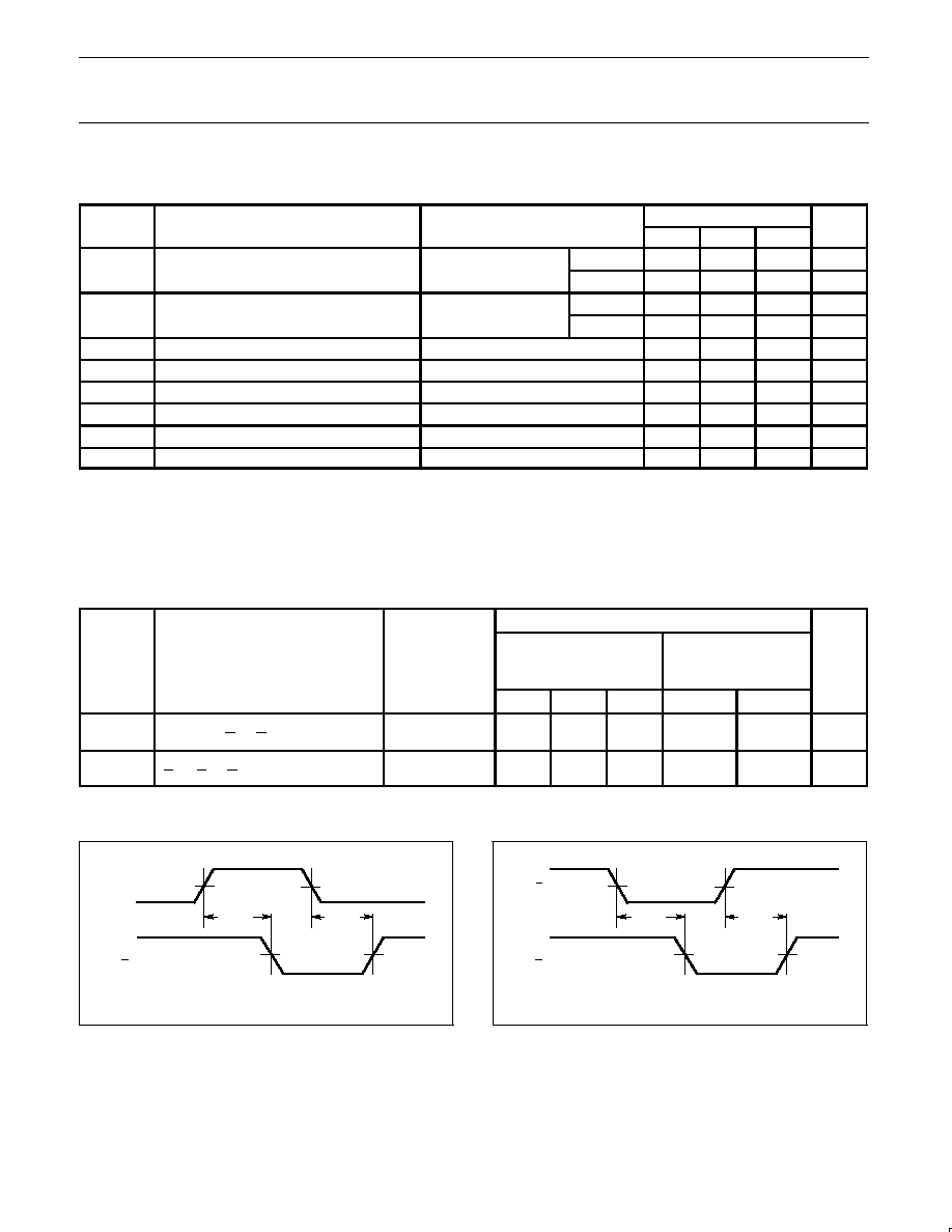
AC WAVEFORMS
For all waveforms, V
M
= 1.5V
VM
VM
VM
VM
Qn
An
tPHL
tPLH
SF00133
Waveform 1.
Propagation Delay for Inverting Outputs
VM
VM
VM
VM
Qn
An, En
tPHL
tPLH
SF00134
Waveform 2.
Propagation Delay for Non-Inverting Outputs
Philips Semiconductors
Product specification
74F139
1-of-4 decoder/demultiplexer
February 23, 1990
5
TEST CIRCUIT AND WAVEFORMS
tw
90%
VM
10%
90%
VM
10%
90%
VM
10%
90%
VM
10%
NEGATIVE
PULSE
POSITIVE
PULSE
tw
AMP (V)
0V
0V
tTHL (tf
)
INPUT PULSE REQUIREMENTS
rep. rate
t
w
t
TLH
t
THL
1MHz
500ns
2.5ns
2.5ns
Input Pulse Definition
VCC
family
74F
D.U.T.
PULSE
GENERATOR
RL
CL
RT
VIN
VOUT
Test Circuit for Totem-Pole Outputs
DEFINITIONS:
R
L
= Load resistor;
see AC ELECTRICAL CHARACTERISTICS for value.
C
L
= Load capacitance includes jig and probe capacitance;
see AC ELECTRICAL CHARACTERISTICS for value.
R
T
= Termination resistance should be equal to Z
OUT
of
pulse generators.
tTHL (tf
)
tTLH (tr
)
tTLH (tr
)
AMP (V)
amplitude
3.0V
1.5V
V
M
SF00006