 | –≠–ª–µ–∫—Ç—Ä–æ–Ω–Ω—ã–π –∫–æ–º–ø–æ–Ω–µ–Ω—Ç: N74F151AD | –°–∫–∞—á–∞—Ç—å:  PDF PDF  ZIP ZIP |
Document Outline
- FEATURES
- DESCRIPTION
- PIN CONFIGURATION
- ORDERING INFORMATION
- INPUT AND OUTPUT LOADING AND FAN-OUT TABLE
- LOGIC SYMBOL
- IEC/IEEE SYMBOL
- LOGIC DIAGRAM
- FUNCTION TABLE
- ABSOLUTE MAXIMUM RATINGS
- RECOMMENDED OPERATING CONDITIONS
- DC ELECTRICAL CHARACTERISTICS
- AC ELECTRICAL CHARACTERISTICS
- AC WAVEFORMS
- TEST CIRCUIT AND WAVEFORMS
- PACKAGE OUTLINES
- Data sheet status
- Definitions
- Disclaimers

Philips
Semiconductors
74F151A
8-input multiplexer
Product specification
Supercedes data of 1989 Mar 03
IC15 Data Handbook
1995 Jul 17
INTEGRATED CIRCUITS
Philips Semiconductors
Product specification
74F151A
8-input multiplexer
2
1995 Jul 17
853≠1158 15459
FEATURES
∑
High speed 8-to-1 multiplexing
∑
On chip decoding
∑
Multifunction capability
∑
Complementary outputs
DESCRIPTION
The 74F151A is a logic implementation of a single-pole, 8-position
switch with the switch position controlled by the state of three Select
(S0, S1, S2) inputs. True (Y) and complementary (Y) outputs are
both provided. The Enable input (E) is active Low. When E is High,
the Y output is High and the Y output is Low, regardless of all other
inputs. In one package the 74F151A provides the ability to select
from eight sources of data or control information. The device can
provide any logic function of four variables and the negation with
correct manipulation.
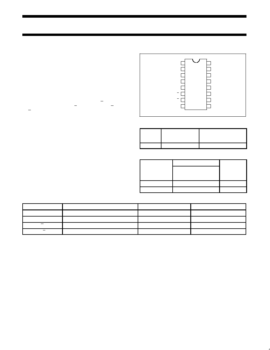
PIN CONFIGURATION
16
15
14
13
12
11
10
7
6
5
4
3
2
1
E
V
CC
I7
S0
S1
I6
I4
I5
I3
I2
Y
I1
I0
Y
9
8
GND
S2
SF00742
TYPE
TYPICAL
PROPAGATION
DELAY
TYPICAL
SUPPLY CURRENT
(TOTAL)
74F151A
4.5ns
17mA
ORDERING INFORMATION
ORDER CODE
DESCRIPTION
COMMERCIAL RANGE
V
CC
= 5V
±
10%,
T
amb
= 0
∞
C to +70
∞
C
PKG DWG #
16-pin plastic DIP
N74F151AN
SOT38-4
16-pin plastic SO
N74F151AD
SOT109-1
INPUT AND OUTPUT LOADING AND FAN-OUT TABLE
PINS
DESCRIPTION
74F (U.L.) HIGH/LOW
LOAD VALUE HIGH/LOW
I0≠I7
Data inputs
1.0/1.0
20
µ
A/0.6mA
S0≠S2
Select inputs
1.0/1.0
20
µ
A/0.6mA
E
Enable input (active High)
1.0/1.0
20
µ
A/0.6mA
Y, Y
Data outputs
150/33
3mA/20mA
NOTE:
One (1.0) FAST unit load is defined as: 20
µ
A in the High state and 0.6mA in the Low state.
Philips Semiconductors
Product specification
74F151A
8-input multiplexer
1995 Jul 17
3
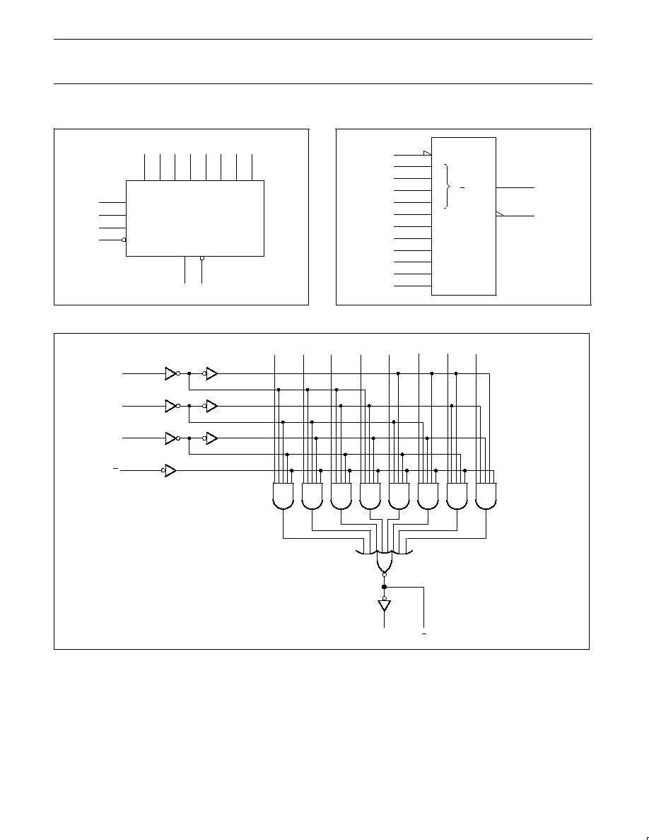
LOGIC SYMBOL
1
2
3
V
CC
= Pin 16
GND = Pin 8
SF00743
6
5
11
10
9
S0
S1
S2
7
4
12
13
14
15
E
Y
Y
I0
I1
I2
I3
I4
I5
I6
I7
IEC/IEEE SYMBOL
SF00744
MUX
7
11
3
2
1
5
6
0
G
0
7
10
2
EN
9
4
14
13
12
15
LOGIC DIAGRAM
9
10
11
V
CC
= Pin 16
GND = Pin 8
SF00741
Y
Y
5
6
4
3
2
1
15
14
13
12
I0
I1
I2
I3
I4
I5
I6
I7
7
E
S0
S1
S2
Philips Semiconductors
Product specification
74F151A
8-input multiplexer
1995 Jul 17
4
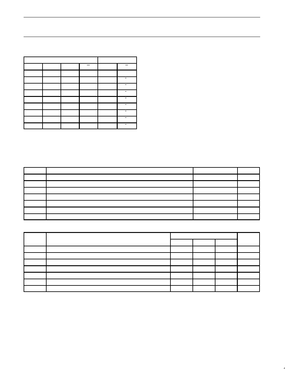
FUNCTION TABLE
INPUTS
OUTPUTS
S2
S1
S0
E
Y
Y
X
X
X
H
L
H
L
L
L
L
I0
I0
L
L
H
L
I1
I1
L
H
L
L
I2
I2
L
H
H
L
I3
I3
H
L
L
L
I4
I4
H
L
H
L
I5
I5
H
H
L
L
I6
I6
H
H
H
L
I7
I7
NOTES:
H = High voltage level
L
= Low voltage level
X = Don't care
ABSOLUTE MAXIMUM RATINGS
(Operation beyond the limit set forth in this table may impair the useful life of the device.
Unless otherwise noted these limits are over the operating free air temperature range.)
SYMBOL
PARAMETER
RATING
UNIT
V
CC
Supply voltage
≠0.5 to +7.0
V
V
IN
Input voltage
≠0.5 to +7.0
V
I
IN
Input current
≠30 to +5
mA
V
OUT
Voltage applied to output in High output state
≠0.5 to V
CC
V
I
OUT
Current applied to output in Low output state
40
mA
T
amb
Operating free-air temperature range
0 to +70
∞
C
T
stg
Storage temperature
≠65 to +150
∞
C
RECOMMENDED OPERATING CONDITIONS
SYMBOL
PARAMETER
LIMITS
UNIT
SYMBOL
PARAMETER
MIN
NOM
MAX
UNIT
V
CC
Supply voltage
4.5
5.0
5.5
V
V
IH
High-level input voltage
2.0
V
V
IL
Low-level input voltage
0.8
V
I
IK
Input clamp current
≠18
mA
I
OH
High-level output current
≠1
mA
I
OL
Low-level output current
20
mA
T
amb
Operating free-air temperature range
0
+70
∞
C

Philips Semiconductors
Product specification
74F151A
8-input multiplexer
1995 Jul 17
5
DC ELECTRICAL CHARACTERISTICS
(Over recommended operating free-air temperature range unless otherwise noted.)
NO TAG
LIMITS
SYMBOL
PARAMETER\
TEST CONDITIONS
NO TAG
MIN
TYP
NO TAG
MAX
UNIT
V
O
High level output voltage
V
CC
= MIN, V
IL
= MAX,
±
10%V
CC
2.5
V
V
OH
High-level output voltage
CC
,
IL
,
V
IH
= MIN, I
OH
= MAX
±
5%V
CC
2.7
3.4
V
V
O
Low level output voltage
V
CC
= MIN, V
IL
= MAX,
±
10%V
CC
0.30
0.50
V
V
OL
Low-level output voltage
CC
,
IL
,
V
IH
= MIN, I
OL
= MAX
±
5%V
CC
0.30
0.50
V
V
IK
Input clamp voltage
V
CC
= MIN, I
I
= I
IK
≠0.73
≠1.2
V
I
I
Input current at maximum input
voltage
V
CC
= MAX, V
I
= 7.0V
100
µ
A
I
IH
High-level input current
V
CC
= MAX, V
I
= 2.7V
20
µ
A
I
IL
Low-level input current
V
CC
= MAX, V
I
= 0.5V
≠0.6
mA
I
OS
Short-circuit output current
NO TAG
V
CC
= MAX
≠60
≠150
mA
I
CC
Supply current (total)
I
CCH
V
CC
= MAX
18
25
mA
I
CC
Supply current (total)
I
CCL
V
CC
= MAX
17
25
mA
NOTES:
1. For conditions shown as MIN or MAX, use the appropriate value specified under recommended operating conditions for the applicable type.
2. All typical values are at V
CC
= 5V, T
amb
= 25
∞
C.
3. Not more than one output should be shorted at a time. For testing I
OS
, the use of high-speed test apparatus and/or sample-and-hold
techniques are preferable in order to minimize internal heating and more accurately reflect operational values. Otherwise, prolonged shorting
of a High output may raise the chip temperature well above normal and thereby cause invalid readings in other parameter tests. In any
sequence of parameter tests, I
OS
tests should be performed last.
AC ELECTRICAL CHARACTERISTICS
LIMITS
SYMBOL
PARAMETER
TEST
CONDITION
V
CC
= +5.0V
T
amb
= +25
∞
C
C
L
= 50pF
R
L
= 500
V
CC
= +5.0V
±
10%
T
amb
= 0
∞
C to +70
∞
C
C
L
= 50pF
R
L
= 500
UNIT
MIN
TYP
MAX
MIN
MAX
t
PLH
t
PHL
Propagation delay
In to Y
Waveform NO TAG
2.5
2.5
4.5
4.5
7.0
7.0
2.5
2.5
7.5
7.5
ns
t
PLH
t
PHL
Propagation delay
In to Y
Waveform NO TAG
2.0
1.0
4.0
2.0
7.0
4.5
2.0
1.0
7.5
5.0
ns
t
PLH
t
PHL
Propagation delay
Sn to Y
Waveform 1, 2
4.5
4.0
6.5
6.0
10.0
8.5
4.0
3.5
11.0
9.5
ns
t
PLH
t
PHL
Propagation delay
Sn to Y
Waveform NO TAG,
NO TAG
3.5
2.5
5.5
4.5
8.5
7.0
3.0
2.0
9.5
7.5
ns
t
PLH
t
PHL
Propagation delay
E to Y
Waveform 1
4.0
3.0
6.5
5.0
9.0
7.0
3.5
3.0
9.5
7.5
ns
t
PLH
t
PHL
Propagation delay
E to Y
Waveform NO TAG
2.5
2.0
4.5
3.5
6.5
5.5
2.5
1.5
7.0
6.0
ns
AC WAVEFORMS
For all waveforms, V
M
= 1.5V