
Philips
Semiconductors
74F157*, 74F157A, 74F158*, 74F158A
Data selectors/multiplexers
Product specification
1996 Mar 12
INTEGRATED CIRCUITS
IC15 Data Handbook
* Discontinued part. Please see the Discontinued Product List in Section 1, page 21.

Philips Semiconductors
Product specification
74F157A, 74F158A
Data selectors/multiplexers
74F157A:
Quad 2-input data selector/multiplexer, non-inverting
74F158A:
Quad 2-input data selector/multiplexer, inverting
2
1996 Mar 12
853-0346 16555
DESCRIPTION
The 74F157A is a high speed Quad 2-Input Multiplexer which
selects 4 bits of data from one of two sources under the control of a
common Select input (S). The Enable input (E) is active when Low.
When E is High, all of the outputs (Yn) are forced Low regardless of
all other input conditions.
Moving data from two registers to a common output bus is a
common use of the 74F157A. The state of the Select input
determines the particular register from which the data comes.
The device is the logic implementation of a 4-pole, 2-position switch
where the position of the switch is determined by the logic levels
supplied to the Select input.
The 74F158A is similar, but has inverting outputs (Yn).
�
Industrial temperature range (�10
�
C to +85
�
C) available for
74F157A
TYPE
TYPICAL
PROPAGATION
DELAY
TYPICAL
SUPPLY CURRENT
(TOTAL)
74F157
4.6ns
15mA
74F157A
4.6ns
15mA
74F158
3.7ns
10mA
74F158A
3.7ns
10mA
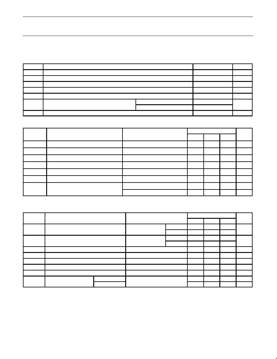
ORDERING INFORMATION
ORDER CODE
DESCRIPTION
COMMERCIAL RANGE
V
CC
= 5V
�
10%, T
amb
= 0
�
C to +70
�
C
INDUSTRIAL RANGE
V
CC
= 5V
�
10%, T
amb
= �40
�
C to +85
�
C
PKG. DWG. #
16-pin plastic DIP
N74F157AN, N174F158AN
I74F157AN
SOT38-4
16-pin plastic SO
N74F157AD, N74F158AD
I74F157AD
SOT109-1
INPUT AND OUTPUT LOADING AND FAN OUT TABLE
PINS
DESCRIPTION
74F (U.L.) HIGH/LOW
LOAD VALUE HIGH/LOW
Ina, Inb, Inc, Ind
Data inputs
1.0/1.0
20
�
A/0.6mA
S
Select input
1.0/1.0
20
�
A/0.6mA
E
Enable input
1.0/1.0
20
�
A/0.6mA
Ya�Yd
Data outputs (74F157/74F157A)
50/33
1.0mA/20mA
Ya�Yd
Data outputs (74F158/74F158A)
50/33
1.0mA/20mA
NOTE: One (1.0) FAST unit load is defined as: 20
�
A in the High state and 0.6mA in the Low state.
PIN CONFIGURATIONS, 74F157A 74F158A
16
15
14
13
12
11
10
7
6
5
4
3
2
1
Yb
V
CC
Yd
I0c
I1c
I1d
E
I0d
S
I0a
I1b
I1a
Ya
I0b
9
8
GND
Yc
SF00215
16
15
14
13
12
11
10
7
6
5
4
3
2
1
Yb
V
CC
Yd
I0c
I1c
I1d
E
I0d
S
I0a
I1b
I1a
Ya
I0b
9
8
GND
Yc
SF00216
LOGIC SYMBOLS, 74F157A 74F158A
V
CC
= Pin 16
GND = Pin 8
SF00217
1
15
S
E
2
3
5
6
11
10
14
I0a
I1a
I0b
I1b
I0c
I1c
I0d
Ya
Yb
Yc
Yd
4
7
9
12
13
I1d
V
CC
= Pin 16
GND = Pin 8
SF00218
1
15
S
E
2
3
5
6
11
10
14
I0a
I1a
I0b
I1b
I0c
I1c
I0d
Ya
Yb
Yc
Yd
4
7
9
12
13
I1d

Philips Semiconductors
Product specification
74F157A, 74F158A
Data selectors/multiplexers
1996 Mar 12
3
IEEE/IEC SYMBOLS, 74F157A 74F158A
SF00219
2
1
1
G1
15
EN
3
4
1
MUX
5
6
7
11
10
9
14
13
12
SF00220
2
1
1
G1
15
EN
3
4
1
MUX
5
6
7
11
10
9
14
13
12
LOGIC DIAGRAM, 74F157A
I0a
I1a
I0b
I1b
I0c
I1c
I0d
I1d
E
S
2
3
5
6
11
10
14
13
15
1
4
7
9
12
Ya
Yb
Yc
Yd
V
CC
= Pin 16
GND = Pin 8
SF00225
FUNCTION TABLE, 74F157A
INPUTS
OUTPUT
E
S
I0n
I1n
Yn
H
X
X
X
L
L
H
X
L
L
L
H
X
H
H
L
L
L
X
L
L
L
H
X
H
H = High voltage level
L = Low voltage level
X = Don't care
74F158A
I0a
I1a
I0b
I1b
I0c
I1c
I0d
I1d
E
S
2
3
5
6
11
10
14
13
15
1
4
7
9
12
Ya
Yb
Yc
Yd
V
CC
= Pin 16
GND = Pin 8
SF00226
74F158A
INPUTS
OUTPUT
E
S
I0n
I1n
Yn
H
X
X
X
H
L
L
L
X
H
L
L
H
X
L
L
H
X
L
H
L
H
X
H
L
H = High voltage level
L = Low voltage level
X = Don't care
Philips Semiconductors
Product specification
74F157A, 74F158A
Data selectors/multiplexers
1996 Mar 12
4
ABSOLUTE MAXIMUM RATINGS
(Operation beyond the limit set forth in this table may impair the useful life of the device.
Unless otherwise noted these limits are over the operating free-air temperature range.)
SYMBOL
PARAMETER
RATING
UNIT
V
CC
Supply voltage
�0.5 to +7.0
V
V
IN
Input voltage
�0.5 to +7.0
V
I
IN
Input current
�30 to +5
mA
V
OUT
Voltage applied to output in High output state
�0.5 to V
CC
V
I
OUT
Current applied to output in Low output state
40
mA
T
b
Operating free-air temperature range
Commercial Range
0 to +70
�
C
T
amb
O erating free-air tem erature range
Industrial Range 74F157A only
�40 to +85
�
C
T
stg
Storage temperature range
�65 to +150
�
C
RECOMMENDED OPERATING CONDITIONS
SYMBOL
PARAMETER
LIMITS
UNIT
SYMBOL
PARAMETER
MIN
NOM
MAX
UNIT
V
CC
Supply voltage
4.5
5.0
5.5
V
V
IH
High-level input voltage
2.0
V
V
IL
Low-level input voltage
0.8
V
I
IK
Input clamp current
�18
mA
I
OH
High-level output current
�1
mA
I
OL
Low-level output current
20
mA
T
Operating free air temperature range
Commercial Range
0
70
T
amb
Operating free air temperature range
Industrial Range 74F157A only
�40
85
�
C
DC ELECTRICAL CHARACTERISTICS
(Over recommended operating free-air temperature range unless otherwise noted.)
SYMBOL
PARAMETER
TEST CONDITIONS
1
LIMITS
UNIT
SYMBOL
PARAMETER
TEST CONDITIONS
1
MIN
TYP
2
MAX
UNIT
V
OH
High-level output voltage
V
CC
= MIN, V
IL
= MAX
�
10%V
CC
2.5
V
V
OH
High-level out ut voltage
V
IH
= MIN, I
OH
= MAX
�
5%V
CC
2.7
3.4
V
V
OL
Low-level output voltage
V
CC
= MIN, V
IL
= MAX
�
10%V
CC
0.30
0.50
V
V
OL
Low-level out ut voltage
V
IH
= MIN, I
OL
= MAX
�
5%V
CC
0.30
0.50
V
V
IK
Input clamp voltage
V
CC
= MIN, I
I
= I
IK
�0.73
�1.2
V
I
I
Input current at maximum input voltage
V
CC
= MAX, V
I
= 7.0V
100
�
A
I
IH
High-level input current
V
CC
= MAX, V
I
= 2.7V
20
�
A
I
IL
Low-level input current
V
CC
= MAX, V
I
= 0.5V
�0.6
mA
I
OS
Short-circuit output current
3
V
CC
= MAX
�60
�150
mA
I
CC
Supply current (total)
4
74F157A
V
CC
= MAX
15.0
23.0
mA
I
CC
Su
ly current (total)
4
74F158A
V
CC
= MAX
14.0
19.0
mA
NOTES:
1. For conditions shown as MIN or MAX, use the appropriate value specified under recommended operating conditions for the applicable type.
2. All typical values are at V
CC
= 5V, T
amb
= 25
�
C.
3. Not more than one output should be shorted at a time. For testing I
OS
, the use of high-speed test apparatus and/or sample-and-hold
techniques are preferable in order to minimize internal heating and more accurately reflect operational values. Otherwise, prolonged shorting
of a High output may raise the chip temperature well above normal and thereby cause invalid readings in other parameter tests. In any
sequence of parameter tests, I
OS
tests should be performed last.
4. I
CC
is measured with 4.5V applied to all inputs and all outputs open.
Philips Semiconductors
Product specification
74F157A, 74F158A
Data selectors/multiplexers
1996 Mar 12
5
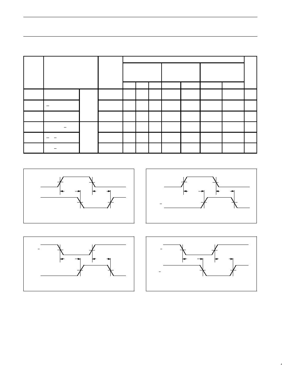
AC ELECTRICAL CHARACTERISTICS FOR 74F157A AND 74F158A
LIMITS
SYMBOL
PARAMETER
TEST
CONDITION
V
CC
= +5.0V
T
amb
= +25
�
C
C
L
= 50pF
R
L
= 500
V
CC
= +5.0V
�
10%
T
amb
= 0
�
C to +70
�
C
C
L
= 50pF
R
L
= 500
V
CC
= +5.0V
�
10%
T
amb
= �40
�
C to +85
�
C
C
L
= 50pF
R
L
= 500
UNIT
MIN
TYP
MAX
MIN
MAX
MIN
MAX
t
PLH
t
PHL
Propagation delay
I0n, I1n to Yn
Waveform 1
3.5
2.5
4.5
3.5
6.5
5.0
3.0
1.5
7.0
6.0
3.0
1.5
7.5
6.5
ns
t
PLH
t
PHL
Propagation delay
E to Yn
74F157A
Waveform 3
6.0
4.0
7.5
5.0
9.0
6.5
5.5
4.0
10.5
7.0
5.5
4.0
11.0
7.5
ns
t
PLH
t
PHL
Propagation delay
S to Yn
Waveform 1
5.5
4.5
7.5
6.0
10.0
7.5
5.0
4.0
11.0
8.5
5.0
4.0
11.5
9.0
ns
t
PLH
t
PHL
Propagation delay
I0n, I1n to Yn
Waveform 2
3.0
1.5
4.0
2.5
6.0
4.0
2.5
1.0
7.0
4.5
--
--
ns
t
PLH
t
PHL
Propagation delay
E to Yn
74F158A
Waveform 4
4.5
5.0
5.5
6.0
7.0
7.5
4.0
5.0
7.5
8.0
--
--
ns
t
PLH
t
PHL
Propagation delay
S to Yn
Waveform 2
4.5
4.0
6.5
5.5
8.5
7.5
4.0
3.5
9.5
8.0
--
--
ns
AC WAVEFORMS
For all waveforms, V
M
= 1.5V
VM
VM
VM
VM
Yn
I0n, I1n, S
tPHL
tPLH
SF00221
Waveform 1.
Propagation Delay for Data and Select to Output
VM
VM
VM
VM
Yn
I0n, I1n, S
tPLH
tPHL
SF00222
Waveform 2.
Propagation Delay for Data and Select to Output
VM
VM
VM
VM
Yn
E
tPLH
tPHL
SF00223
Waveform 3.
Propagation Delay for Enable to Output
VM
VM
VM
VM
Yn
E
tPHL
tPLH
SF00224
Waveform 4.
Propagation Delay for Enable to Output