 | –≠–ª–µ–∫—Ç—Ä–æ–Ω–Ω—ã–π –∫–æ–º–ø–æ–Ω–µ–Ω—Ç: N74F169D | –°–∫–∞—á–∞—Ç—å:  PDF PDF  ZIP ZIP |
Document Outline
- FEATURES
- DESCRIPTION
- PIN CONFIGURATION
- ORDERING INFORMATION
- INPUT AND OUTPUT LOADING AND FAN-OUT TABLE
- LOGIC SYMBOL
- LOGIC SYMBOL (IEEE/IEC)
- FUNCTIONAL DESCRIPTION
- MODE SELECT Ñ FUNCTION TABLE
- MODE SELECT TABLE
- STATE DIAGRAM
- LOGIC DIAGRAM
- APPLICATION
- ABSOLUTE MAXIMUM RATINGS
- RECOMMENDED OPERATING CONDITIONS
- DC ELECTRICAL CHARACTERISTICS
- AC ELECTRICAL CHARACTERISTICS
- AC SETUP REQUIREMENTS
- AC WAVEFORMS
- TIMING DIAGRAM
- TEST CIRCUIT AND WAVEFORM
- PACKAGE OUTLINE
- DEFINITIONS
Philips
Semiconductors
74F168*, 74F169
4-bit up/down binary synchronous counter
Product specification
1996 Jan 05
INTEGRATED CIRCUITS
IC15 Data Handbook
* Discontinued part. Please see the Discontinued Product List in Section 1, page 21.
Philips Semiconductors
Product specification
74F169
4-bit up/down binary synchronous counter
2
1996 Jan 05
853≠0350 16190
FEATURES
∑
Synchronous counting and loading
∑
Up/Down counting
∑
Modulo 16 binary counter
∑
Two Count Enable inputs for n-bit cascading
∑
Positive edge-triggered clock
∑
Built-in carry look-ahead capability
∑
Presettable for programmable operation
DESCRIPTION
The 74F169 is a 4-bit synchronous, presettable Modulo 16 up/down
counter featuring an internal carry look-ahead for applications in
high-speed counting designs. Synchronous operation is provided by
having all flip-flops clocked simultaneously so that the outputs
change coincident with each other when instructed by the Count
Enable inputs and internal gating. This mode of operation eliminates
the output spikes which are normally associated with asynchronous
(ripple clock) counters. A buffered clock input triggers the flip-flops
on the Low-to-High transition of the clock.
The counter is fully programmable; that is, the outputs may be
preset to either level.
Presetting is synchronous with the clock and takes place regardless
of the levels of the Count Enable inputs. A Low level on the Parallel
Enable (PE) input disables the counter and causes the data at the
D
n
input to be loaded into the counter on the next Low-to-High
transition of the clock.
The direction of counting is controlled by the Up/Down (U/D) input; a
High will cause the count to increase, a Low will cause the count to
decrease.
The carry look-ahead circuitry provides for n-bit synchronous
applications without additional gating. Instrumental in accomplishing
this function are two Count Enable inputs (CET
,
CEP) and a
Terminal Count (TC) output. Both Count Enable inputs must be Low
to count. The CET input is fed forward to enable the TC output. The
TC output thus enabled will produce a Low output pulse with a
duration approximately equal to the High level portion of the Q
0
output. The Low level TC pulse is used to enable successive
cascaded stages.
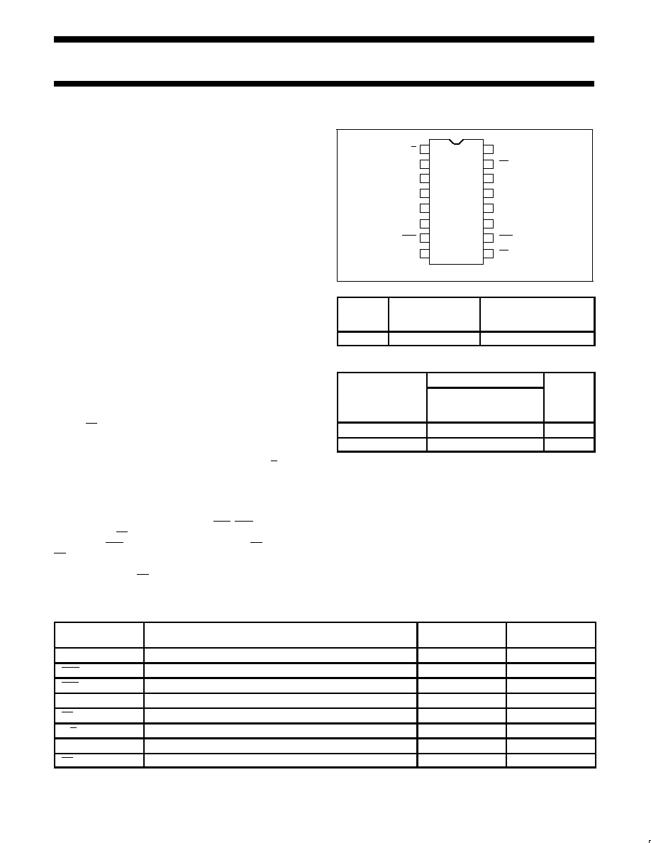
PIN CONFIGURATION
16
15
14
13
12
11
10
9
8
7
6
5
4
3
2
1
VCC
TC
Q0
Q1
Q2
Q3
CET
PE
U/D
CP
D0
D1
D2
D3
CEP
GND
SF00766
TYPE
TYPICAL f
MAX
TYPICAL
SUPPLY CURRENT
(TOTAL)
74F169
115MHz
35mA
ORDERING INFORMATION
ORDER CODE
DESCRIPTION
COMMERCIAL RANGE
V
CC
= 5V
±
10%,
T
amb
= 0
∞
C to +70
∞
C
PKG
DWG #
16-pin plastic DIP
N74F169N
SOT38-4
16-pin plastic SO
N74F169D
SOT109-1
INPUT AND OUTPUT LOADING AND FAN-OUT TABLE
PINS
DESCRIPTION
74F(U.L.)
HIGH/LOW
LOAD VALUE
HIGH/LOW
D
0
- D
3
Parallel data inputs
1.0/1.0
20
µ
A/0.6mA
CEP
Count Enable parallel input (active Low)
1.0/1.0
20
µ
A/0.6mA
CET
Count Enable Trickle input (active Low)
1.0/2.0
20
µ
A/1.2mA
CP
Clock input (active rising edge)
1.0/1.0
20
µ
A/0.6mA
PE
Parallel Enable input (active Low)
1.0/1.0
20
µ
A/0.6mA
U/D
Up/Down count control input
1.0/1.0
20
µ
A/0.6mA
Q
0
- Q
3
Flip-flop outputs
50/33
1.0mA/20mA
TC
Terminal count output (active Low)
50/33
1.0mA/20mA
NOTE: One (1.0) FAST Unit Load (U.L.) is defined as: 20
µ
A in the High state and 0.6mA in the Low state.
Philips Semiconductors
Product specification
74F169
4-bit up/down binary synchronous counter
1996 Jan 05
3
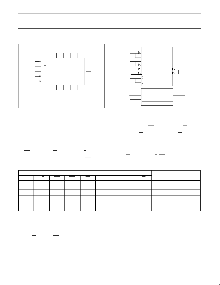
LOGIC SYMBOL
9
3
4
5
6
15
11
12
13
14
1
2
7
10
CP
CEP
CET
PE
D0
D1
D2
D3
Q0
Q1
Q2
Q3
TC
U/D
SF00786
V
CC
= Pin 16
GND = Pin 8
LOGIC SYMBOL (IEEE/IEC)
M4 [DOWN]
9
1
10
7
2
[1]
3
4
5
6
1, 7D
14
13
12
11
M1 [LOAD]
SF00787
M2 [COUNT]
M3 [UP]
CTR DIV 16
[2]
[4]
[8]
15
3, 5 CT=15
4, 5 CT=0
G5
G6
2, 3, 5, 6+/C7
2, 4, 5, 6≠
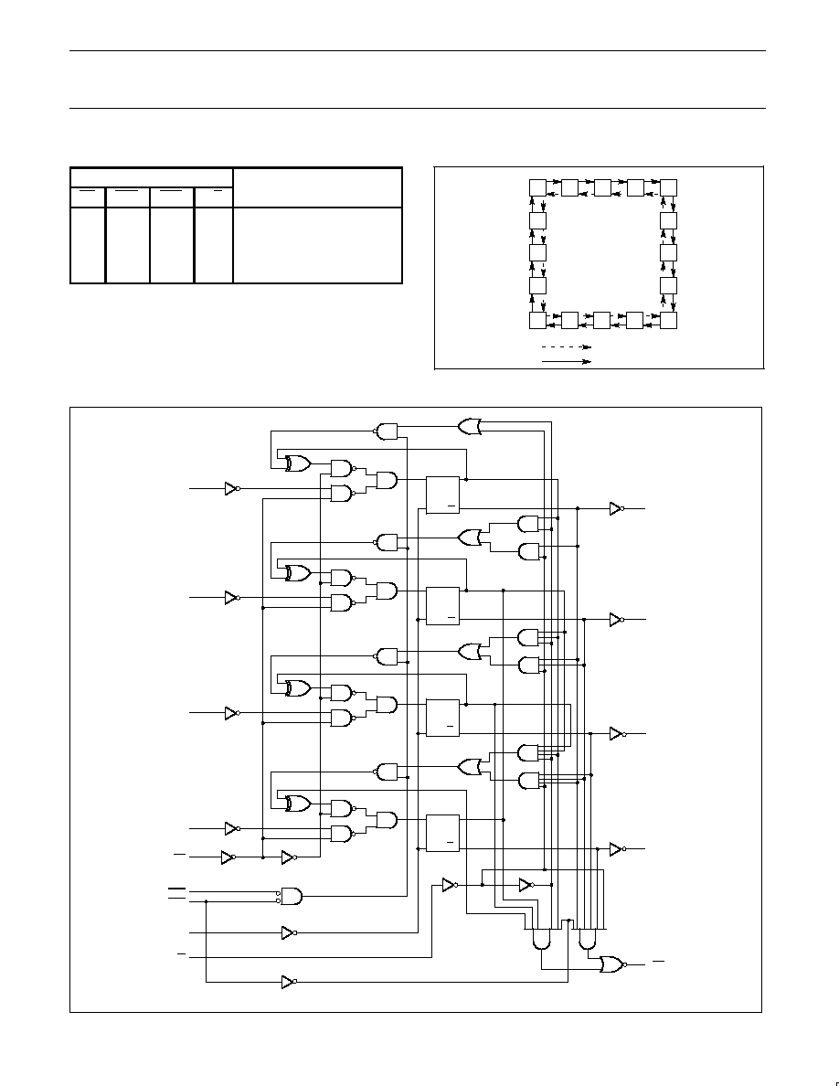
FUNCTIONAL DESCRIPTION
The 74F169 uses edge-triggered J-K-type flip-flops and have no
constraints on changing the control or data input signals in either
state of the clock. The only requirement is that the various inputs
attain the desired state at least a setup time before the rising edge
of the clock and remain valid for the recommended hold time
thereafter. The parallel load operation takes precedence over the
other operations, as indicated in the Mode Select Table. When PE is
Low, the data on the D
0
- D
3
inputs enter the flip-flops on the next
rising edge of the Clock. In order for counting to occur, both CEP
and CET must be Low and PE must be High; the U/D input
determines the direction of counting. The Terminal Count (TC)
output is normally High and goes Low, provided that CET is Low,
when a counter reaches zero in the Count Down mode or reaches
15 in the Count Up mode. The TC output state is not a function of
the Count Enable Parallel (CEP) input level. Since the TC signal is
derived by decoding the flip-flop states, there exists the possibility of
decoding spikes on TC. For this reason the use of TC as a clock
signal is not recommended (see logic equations below).
1) Count Enable = CEP
CET
PE
2) Up: TC = Q
0
Q
3
(U/D)
CET
3) Down: TC = Q
0
Q
1
Q
2
Q
3
(U/D)
CET
MODE SELECT -- FUNCTION TABLE
INPUTS
OUTPUTS
OPERATING MODE
CP
U/D
CEP
CET
PE
D
n
Q
n
TC
OPERATING MODE
X
X
X
l
l
L
(1)
Parallel load (Dn
Qn)
X
X
X
X
X
H
(1)
h
l
l
h
X
Count Up
(1)
Count Up (increment)
l
l
l
h
X
Count Down
(1)
Count Down (decrement)
X
h
X
h
X
q
n
(1)
Hold (do nothing)
X
X
X
h
X
q
n
H
H = High voltage level steady state
h = High voltage level one setup time prior to the Low-to-High clock transition
L = Low voltage level steady state
l
= Low voltage level one setup time prior to the Low-to-High clock transition
q = Lower case letters indicate the state of the referenced output prior to the Low-to-High clock transition
X = Don't care
= Low-to-High clock transition
(1) = The TC is Low when CET is Low and the counter is at Terminal Count.
Terminal Count Up is (HHHH) and Terminal Count Down is (LLLL).
Philips Semiconductors
Product specification
74F169
4-bit up/down binary synchronous counter
1996 Jan 05
4
MODE SELECT TABLE
INPUTS
OPERATING MODE
PE
CEP
CET
U/D
OPERATING MODE
L
X
X
X
Load (D
n
Q
n
)
H
L
L
H
Count Up (Increment)
H
L
L
L
Count Down (Decrement)
H
H
X
X
No Change (Hold)
H
X
H
X
No Change (Hold)
H = High Voltage
L = Low Voltage Level
X = Don't care
STATE DIAGRAM
0
1
2
3
4
5
6
7
8
9
10
11
12
13
14
15
COUNT DOWN
COUNT UP
SF00788
LOGIC DIAGRAM
D
CP
Q
Q
D
CP
Q
Q
D
CP
Q
Q
D
CP
Q
Q
3
4
5
6
9
7
10
2
1
15
11
12
13
14
Q0
Q1
Q2
Q3
CP
D3
D2
D1
D0
U/D
PE
CEP
CET
TC
V
CC
= Pin 16
GND = Pin 8
SF00789
Philips Semiconductors
Product specification
74F169
4-bit up/down binary synchronous counter
1996 Jan 05
5
APPLICATION
CP
CEP
CET
PE
D0 D1 D2 D3
Q0 Q1 Q2 Q3
TC
U/D
CP
CEP
CET
PE
D0 D1 D2 D3
Q0 Q1 Q2 Q3
TC
U/D
CP
CEP
CET
PE
D0 D1 D2 D3
Q0 Q1 Q2 Q3
TC
U/D
CP
CEP
CET
PE
D0 D1 D2 D3
Q0 Q1 Q2 Q3
TC
U/D
CP
U/D
PE
LEAST SIGNIFICANT
4-BIT COUNTER
MOST SIGNIFICANT
4-BIT COUNTER
SF00790
Figure 1. Synchronous Multistage Counting Scheme
ABSOLUTE MAXIMUM RATINGS
(Operation beyond the limits set forth in this table may impair the useful life of the device.
Unless otherwise noted these limits are over the operating free-air temperature range.)
SYMBOL
PARAMETER
RATING
UNIT
V
CC
Supply voltage
≠0.5 to +7.0
V
V
IN
Input voltage
≠0.5 to +7.0
V
I
IN
Input current
≠30 to +5
mA
V
OUT
Voltage applied to output in High output state
≠0.5 to +V
CC
V
I
OUT
Current applied to output in Low output state
40
mA
T
amb
Operating free-air temperature range
0 to +70
∞
C
T
STG
Storage temperature
≠65 to +150
∞
C
RECOMMENDED OPERATING CONDITIONS
SYMBOL
PARAMETER
LIMITS
UNIT
Min
Nom
Max
V
CC
Supply voltage
4.5
5.0
5.5
V
V
IH
High-level input voltage
2.0
V
V
IL
Low-level input voltage
0.8
V
I
IK
Input clamp current
≠18
mA
I
OH
High-level output current
≠1
mA
I
OL
Low-level output current
20
mA
T
amb
Operating free-air temperature range
0
70
∞
C
Philips Semiconductors
Product specification
74F169
4-bit up/down binary synchronous counter
1996 Jan 05
6
DC ELECTRICAL CHARACTERISTICS
(Over recommended operating free-air temperature range unless otherwise noted.)
NO TAG
LIMITS
SYMBOL
PARAMETER
TEST CONDITIONS
NO TAG
MIN
TYP
NO TAG
MAX
UNIT
V
O
High level output voltage
V
CC
= MIN, V
IL
= MAX,
±
10%V
CC
2.5
V
V
OH
High-level output voltage
CC
,
IL
,
V
IH
= MIN, I
OH
= MAX
±
5%V
CC
2.7
3.4
V
V
O
Low level output voltage
V
CC
= MIN, V
IL
= MAX,
±
10%V
CC
0.35
0.50
V
V
OL
Low-level output voltage
CC
,
IL
,
V
IH
= MIN, I
OL
= MAX
±
5%V
CC
0.35
0.50
V
V
IK
Input clamp voltage
V
CC
= MIN, I
I
= I
IK
≠0.73
≠1.2
V
I
I
Input current at maximum input
voltage
V
CC
= MAX, V
I
= 7.0V
100
µ
A
I
IH
High-level input current
V
CC
= MAX, V
I
= 2.7V
20
µ
A
I
Low level input current
CET
V
CC
= MAX, V
I
= 0.5V
≠1.2
mA
I
IL
Low-level input current
Others
V
CC
= MAX, V
I
= 0.5V
≠0.6
mA
I
OS
Short-circuit output current
NO TAG
V
CC
= MAX
≠60
≠150
mA
I
CC
Supply current (total)
4
V
CC
= MAX
35
52
mA
NOTES:
1. For conditions shown as MIN or MAX, use the appropriate value specified under recommended operating conditions for the applicable type.
2. All typical values are at V
CC
= 5V, T
amb
= 25
∞
C.
3. Not more than one output should be shorted at a time. For testing I
OS
, the use of high-speed test apparatus and/or sample-and-hold
techniques are preferable in order to minimize internal heating and more accurately reflect operational values. Otherwise, prolonged shorting
of a High output may raise the chip temperature well above normal and thereby cause invalid readings in other parameter tests. In any
sequence of parameter tests, I
OS
tests should be performed last.
4. I
CC
is measured after applying a momentary 4.5V, then ground to the clock input with all other inputs grounded and all outputs open.
Philips Semiconductors
Product specification
74F169
4-bit up/down binary synchronous counter
1996 Jan 05
7
AC ELECTRICAL CHARACTERISTICS
LIMITS
T
amb
= +25
∞
C
T
amb
= 0
∞
C to +70
∞
C
SYMBOL
PARAMETER
TEST CONDITIONS
V
CC
= +5V
V
CC
= +5V
±
10%
UNIT
C
L
= 50pF, R
L
= 500
C
L
= 50pF, R
L
= 500
MIN
TYP
MAX
MIN
MAX
f
MAX
Maximum clock frequency
Waveform 1
100
115
90
MHz
t
PLH
t
PHL
Propagation delay
CP to Q
n
(PE, High or Low)
Waveform 1
3.0
4.0
6.5
9.0
8.5
11.5
3.0
4.0
9.5
13.0
ns
ns
t
PLH
t
PHL
Propagation delay
CP to TC
Waveform 1
5.5
4.0
12.0
8.5
15.5
11.0
5.5
4.0
17.0
12.5
ns
ns
t
PLH
t
PHL
Propagation delay
CET to TC
Waveform 2
2.5
2.5
4.5
6.0
6.0
8.0
2.5
2.5
7.0
9.0
ns
ns
t
PLH
t
PHL
Propagation delay
U/D to TC
Waveform 3
3.5
4.0
8.5
8.0
15.0
10.5
3.5
4.0
15.5
12.0
ns
ns
AC SETUP REQUIREMENTS
LIMITS
LIMITS
T
amb
= +25
∞
C
T
amb
= 0
∞
C to +70
∞
C
SYMBOL
PARAMETER
TEST CONDITIONS
V
CC
= +5.0V
V
CC
= +5.0V
±
10%
UNIT
C
L
= 50pF, R
L
= 500
C
L
= 50pF, R
L
= 500
MIN
TYP
MIN
MAX
t
s
(H)
t
s
(L)
Setup time, High or Low
D
n
to CP
Waveform 4
4.0
4.0
4.5
4.5
ns
ns
t
h
(H)
t
h
(L)
Hold time, High or Low
D
n
to CP
Waveform 4
3.0
3.0
3.5
3.5
ns
ns
t
s
(H)
t
s
(L)
Set-up time, High or Low
CEP or CET to CP
Waveform 5
5.0
5.0
5.5
5.5
ns
ns
t
h
(H)
t
h
(L)
Hold time, High or Low
CEP or CET to CP
Waveform 5
0
0
0
0
ns
ns
t
s
(H)
t
s
(L)
Set-up time, High or Low
PE to CP
Waveform 4
8.0
8.0
9.0
9.0
ns
ns
t
h
(H)
t
h
(L)
Hold time, High or Low
PE to CP
Waveform 4
0
0
0
0
ns
ns
t
s
(H)
t
s
(L)
Set-up time, High or Low
U/D to CP
Waveform 6
11.0
7.0
12.5
8.0
ns
ns
t
h
(H)
t
h
(L)
Hold time, High or Low
U/D to CP
Waveform 6
0
0
0
0
ns
ns
t
w
(H)
t
w
(L)
CP
U
or CP
D
pulse width,
High or Low
Waveform 1
5.0
5.0
5.5
5.5
ns
ns
Philips Semiconductors
Product specification
74F169
4-bit up/down binary synchronous counter
1996 Jan 05
8
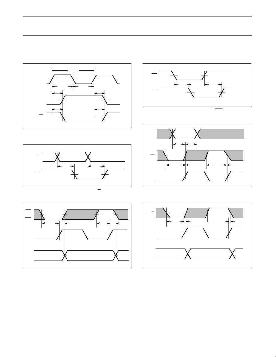
AC WAVEFORMS
For all waveforms, V
M
= 1.5V
The shaded areas indicate when the input is permitted to change for predictable output performance.
t
PHL
V
M
t
PHL
V
M
V
M
V
M
1/f
MAX
t
W
(L)
CP
Q
n
t
W
(H)
V
M
V
M
t
PLH
t
PLH
V
M
TC
SF00791A
Waveform 1. Propagation Delay, Clock Input to Output,
Clock Pulse Width, and Maximum Clock Frequency
V
M
V
M
V
M
t
PLH
t
PHL
V
M
U/D
TC
SF00793
Waveform 3. Propagation Delay U/D Input to
Terminal Count Output
t
s
(L)
CPn
Q
n
V
M
V
M
V
M
V
M
t
h
(L)
t
h
(H)
CEP
CET
t
s
(H)
NO
CHANGE
V
M
V
M
COUNT
V
M
V
M
NO CHANGE
SF00795
Waveform 5. Count Enable Setup and Hold Times
V
M
V
M
V
M
V
M
t
PLH
t
PHL
CET
TC
SF00792
Waveform 2. Propagation Delays CET Input to
Terminal Count Output
t
h
CPn
V
M
V
M
V
M
V
M
V
M
V
M
t
s
t
s
(L)
t
s
(H)
t
h
= 0
D
n
PE
V
M
V
M
t
h
= 0
SF00794
Waveform 4. Parallel Data and Parallel Enable
Setup and Hold Times
t
s
(L)
Q
n
CPn
V
M
V
M
V
M
V
M
t
h
(L)
t
h
(H)
U/D
t
s
(H)
V
M
V
M
COUNT UP
COUNT DOWN
SF00796
Waveform 6. Up/Down Control Setup and Hold Times
Philips Semiconductors
Product specification
74F169
4-bit up/down binary synchronous counter
1996 Jan 05
9
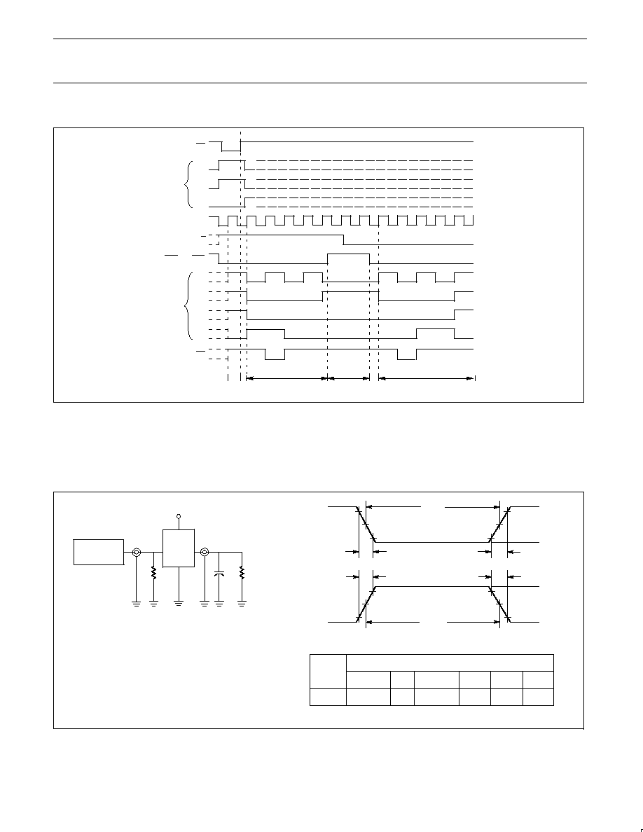
TIMING DIAGRAM (Typical Load, Count, and Inhibit Sequences)
}
7
8
9
0
1
2
2
1
0
9
8
7
COUNT UP
COUNT DOWN
INHIBIT
LOAD
PE
TC
CEP and CET
U/D
D0
D1
D2
D3
Q0
Q1
Q2
Q3
CP
2
SEQUENCE
SF00797
NOTES:
The operation of the 74F169 is similar to the Illustration above.
1. Load (preset) to BCD seven
2. Count up to eight, nine (maximum), zero, one, and two
3. Inhibit
4. Count down to one, zero (minimum), nine, eight, and seven
TEST CIRCUIT AND WAVEFORM
tw
90%
VM
10%
90%
VM
10%
90%
VM
10%
90%
VM
10%
NEGATIVE
PULSE
POSITIVE
PULSE
tw
AMP (V)
0V
0V
tTHL (tf
)
INPUT PULSE REQUIREMENTS
rep. rate
t
w
t
TLH
t
THL
1MHz
500ns
2.5ns
2.5ns
Input Pulse Definition
VCC
family
74F
D.U.T.
PULSE
GENERATOR
RL
CL
RT
VIN
VOUT
Test Circuit for Totem-Pole Outputs
DEFINITIONS:
R
L
= Load resistor;
see AC ELECTRICAL CHARACTERISTICS for value.
C
L
= Load capacitance includes jig and probe capacitance;
see AC ELECTRICAL CHARACTERISTICS for value.
R
T
= Termination resistance should be equal to Z
OUT
of
pulse generators.
tTHL (tf
)
tTLH (tr
)
tTLH (tr
)
AMP (V)
amplitude
3.0V
1.5V
V
M
SF00006
Philips Semiconductors
Product specification
74F168*, 74F169
4-bit up/down binary synchronous counter
1996 Jan 05
10
* Discontinued part. Please see the Discontinued Product List in Section 1, page 21.
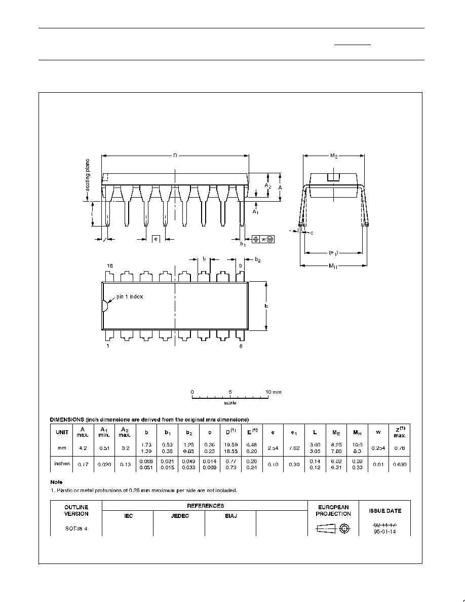
DIP16:
plastic dual in-line package; 16 leads (300 mil)
SOT38-4

Philips Semiconductors
Product specification
74F168*, 74F169
4-bit up/down binary synchronous counter
1996 Jan 05
11
* Discontinued part. Please see the Discontinued Product List in Section 1, page 21.
SO16:
plastic small outline package; 16 leads; body width 3.9 mm
SOT109-1
Philips Semiconductors
Product specification
74F168*, 74F169
4-bit up/down binary synchronous counter
* Discontinued part. Please see the Discontinued Product List in Section 1, page 21.
Philips Semiconductors and Philips Electronics North America Corporation reserve the right to make changes, without notice, in the products,
including circuits, standard cells, and/or software, described or contained herein in order to improve design and/or performance. Philips
Semiconductors assumes no responsibility or liability for the use of any of these products, conveys no license or title under any patent, copyright,
or mask work right to these products, and makes no representations or warranties that these products are free from patent, copyright, or mask
work right infringement, unless otherwise specified. Applications that are described herein for any of these products are for illustrative purposes
only. Philips Semiconductors makes no representation or warranty that such applications will be suitable for the specified use without further testing
or modification.
LIFE SUPPORT APPLICATIONS
Philips Semiconductors and Philips Electronics North America Corporation Products are not designed for use in life support appliances, devices,
or systems where malfunction of a Philips Semiconductors and Philips Electronics North America Corporation Product can reasonably be expected
to result in a personal injury. Philips Semiconductors and Philips Electronics North America Corporation customers using or selling Philips
Semiconductors and Philips Electronics North America Corporation Products for use in such applications do so at their own risk and agree to fully
indemnify Philips Semiconductors and Philips Electronics North America Corporation for any damages resulting from such improper use or sale.
This data sheet contains preliminary data, and supplementary data will be published at a later date. Philips
Semiconductors reserves the right to make changes at any time without notice in order to improve design
and supply the best possible product.
Philips Semiconductors
811 East Arques Avenue
P.O. Box 3409
Sunnyvale, California 94088≠3409
Telephone 800-234-7381
DEFINITIONS
Data Sheet Identification
Product Status
Definition
Objective Specification
Preliminary Specification
Product Specification
Formative or in Design
Preproduction Product
Full Production
This data sheet contains the design target or goal specifications for product development. Specifications
may change in any manner without notice.
This data sheet contains Final Specifications. Philips Semiconductors reserves the right to make changes
at any time without notice, in order to improve design and supply the best possible product.
Philips Semiconductors and Philips Electronics North America Corporation
register eligible circuits under the Semiconductor Chip Protection Act.
©
Copyright Philips Electronics North America Corporation 1996
All rights reserved. Printed in U.S.A.
(print code)
Date of release: July 1994
Document order number:
9397-750-05087