 | –≠–ª–µ–∫—Ç—Ä–æ–Ω–Ω—ã–π –∫–æ–º–ø–æ–Ω–µ–Ω—Ç: N74F173D | –°–∫–∞—á–∞—Ç—å:  PDF PDF  ZIP ZIP |

Philips
Semiconductors
74F173
Quad D-type flip-flop (3-State)
Product specification
IC15 Data Handbook
1990 Aug 31
INTEGRATED CIRCUITS
Philips Semiconductors
Product specification
74F173
Quad D-type flip≠flop (3-State)
2
August 31, 1990
853≠1160 00286
FEATURES
∑
Edge≠triggered D≠type register
∑
Gated clock enable for hold "do nothing" mode
∑
3≠state output buffers
∑
Gated output enable control
∑
Speed upgrade of N8T10 and current sink upgrade
∑
Controlled output edges to minimize ground bounces
∑
48mA sinking capability
DESCRIPTION
The 74F173 is a high speed 4≠bit parallel load register with
clock enable control, 3≠state buffered outputs, and master
reset (MR). When the two clock enable (E0 and E1) inputs
are low, the data on the D inputs is loaded into the register
simultaneously with low≠to≠high clock (CP) transition. When
one or both enable inputs are high one setup time before the
low≠to≠high clock transition, the register retains the previous
data.
Data inputs and clock enable inputs are fully edge≠triggered
and must be stable only one setup time before the
low≠to≠high clock transition.
The master reset (MR) is an active≠high asynchronous
input. When the MR is high, all four flip≠flops are reset
(cleared) independently of any other input condition.
The 3≠state output buffers are controlled by a 2≠input NOR
gate. When both output enable (OE0 and OE1) inputs are
low, the data in the register is presented at the Q output.
When one or both OE inputs are high, the outputs are forced
to a high impedance "off" state.
The 3≠state output buffers are completely independent of
the register operation; the OE transition does not affect the
clock and reset operations.
TYPE
TYPICAL f
max
TYPICAL SUPPLY CURRENT (TOTAL)
74F173
125MHz
23mA
ORDERING INFORMATION
ORDER CODE
DESCRIPTION
COMMERCIAL RANGE
V
CC
= 5V
±
10%, T
amb
= 0
∞
C to +70
∞
C
PKG DWG #
16≠pin plastic DIP
N74F173N
SOT38-4
16≠pin plastic SO
N74F173D
SOT109-1
INPUT AND OUTPUT LOADING AND FAN OUT TABLE
PINS
DESCRIPTION
74F (U.L.) HIGH/
LOW
LOAD VALUE
HIGH/LOW
D0 ≠ D3
Data inputs
1.0/1.0
20
µ
A/0.6mA
CP
Clock input
1.0/1.0
20
µ
A/0.6mA
E0, E1
Clock enable inputs
1.0/1.0
20
µ
A/0.6mA
MR
Master reset input
1.0/1.0
20
µ
A/0.6mA
OE0, OE1
Output enable inputs
1.0/1.0
20
µ
A/0.6mA
Q0 ≠ Q3
Data outputs
750/80
15mA/48mA
Note to input and output loading and fan out table
1. One (1.0) FAST unit load is defined as: 20
µ
A in the high state and 0.6mA in the low state.
Philips Semiconductors
Product specification
74F173
Quad D-type flip≠flop (3-State)
August 31, 1990
3
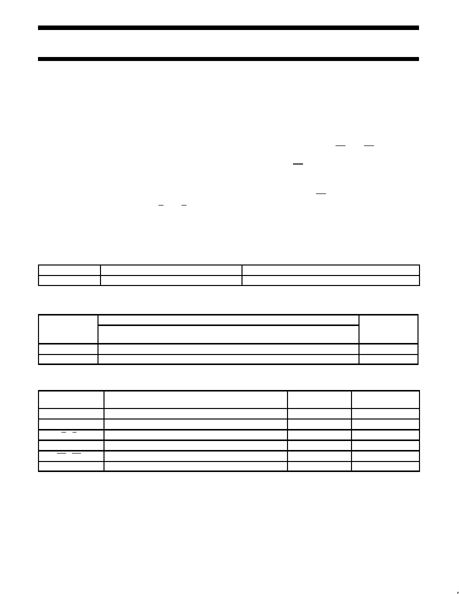
PIN CONFIGURATION
16
15
14
13
12
11
10
7
6
5
4
3
2
1
9
8
VCC
OE0
OE1
Q0
Q1
Q2
Q3
CP
GND
MR
D0
D3
D2
Q2
E1
E0
SF00290
LOGIC SYMBOL
Q0 Q1 Q2 Q3
VCC = Pin 16
GND = Pin 8
D0 D1 D2 D3
14 13 12 11
E0
E1
CP
MR
OE0
OE1
9
10
7
15
1
2
3
4
5
6
SF00291
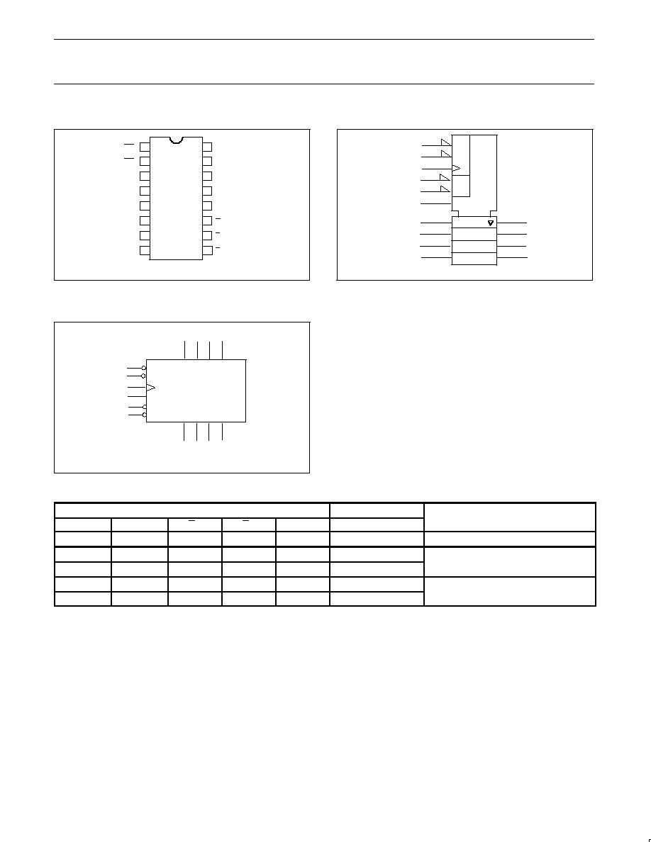
IEC/IEEE SYMBOL
14
13
12
11
&
9
10
7
1
2
15
1D
C1
&
R
3
4
5
6
EN
SF00292
FUNCTION TABLE
INPUTS
OUTPUTS
OUTPUTS
MR
CP
E0
E1
Dn
Qn (register)
H
X
X
X
X
L
Reset (clear)
L
l
l
l
L
Parallel load
L
l
l
h
H
L
X
h
X
X
qn
Hold (do nothing)
L
X
X
h
X
qn
Notes to function table
H = High≠voltage level
h
= High state one setup time before the low≠to≠high clock transition
L
= Low≠voltage level
l
= Low state one setup time before the low≠to≠high clock transition
qn = Lower case letters indicate the state of the referenced input (or output) on setup time prior to the low≠to≠high clock transition
X = Don't care
= Low≠to≠high clock transition
Philips Semiconductors
Product specification
74F173
Quad D-type flip≠flop (3-State)
August 31, 1990
4
FUNCTION TABLE
INPUTS
OUTPUTS
OUTPUTS
Qn (register)
OE0
OE1
Qn
L
L
L
L
Read
H
L
L
H
X
H
X
Z
Disabled
X
X
H
Z
Notes to function table
H = High≠voltage level
L
= Low≠voltage level
X = Don't care
Z = High impedance "off" state
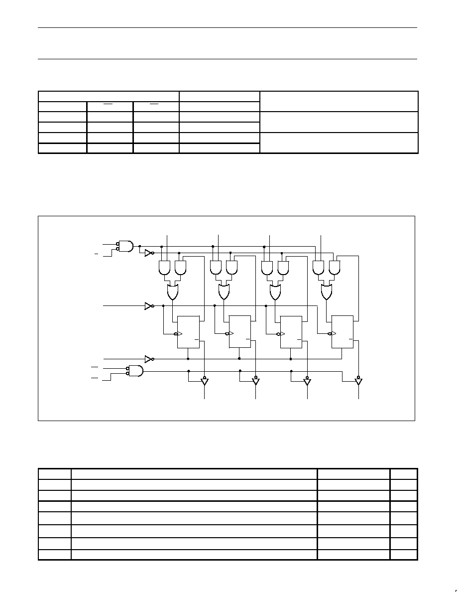
LOGIC DIAGRAM
VCC = Pin 16
GND = Pin 8
D
CP
Q
Q0
3
D0
14
MR
15
Q
RD
D
CP
Q
Q1
4
D1
13
Q
RD
D
CP
Q
Q2
5
D2
12
Q
RD
D
CP
Q
Q3
6
D3
11
Q
RD
1
2
OE0
OE1
E0
E1
9
10
CP
7
SF00293
ABSOLUTE MAXIMUM RATINGS
(Operation beyond the limit set forth in this table may impair the useful life of the device. Unless otherwise noted these limits are over the
operating free air temperature range.)
SYMBOL
PARAMETER
RATING
UNIT
V
CC
Supply voltage
≠0.5 to +7.0
V
V
IN
Input voltage
≠0.5 to +7.0
V
I
IN
Input current
≠30 to +5
mA
V
OUT
Voltage applied to output in high output state
≠0.5 to V
CC
V
I
OUT
Current applied to output in low output state
96
mA
T
amb
Operating free air temperature range
0 to +70
∞
C
T
stg
Storage temperature range
≠65 to +150
∞
C

Philips Semiconductors
Product specification
74F173
Quad D-type flip≠flop (3-State)
August 31, 1990
5
RECOMMENDED OPERATING CONDITIONS
SYMBOL
PARAMETER
LIMITS
UNIT
MIN
NOM
MAX
V
CC
Supply voltage
4.5
5.0
5.5
V
V
IH
High≠level input voltage
2.0
V
V
IL
Low≠level input voltage
0.8
V
I
Ik
Input clamp current
≠18
mA
I
OH
High≠level output current
≠15
mA
I
OL
Low≠level output current
48
mA
T
amb
Operating free air temperature range
0
+70
∞
C
DC ELECTRICAL CHARACTERISTICS
(Over recommended operating free-air temperature range unless otherwise noted.)
SYMBOL
PARAMETER
TEST
LIMITS
UNIT
CONDITIONS
1
MIN
TYP
2
MAX
V
CC
= MIN, V
IL
= MAX,
±
10%V
CC
2.4
V
V
OH
High-level output voltage
V
IH
= MIN, I
OH
= MAX
±
5%V
CC
2.7
3.4
V
V
CC
= MIN, V
IL
= MAX,
±
10%V
CC
2.0
V
V
IH
= MIN, I
OH
= ≠15mA
±
5%V
CC
2.0
3.1
V
V
OL
Low-level output voltage
V
CC
= MIN, V
IL
= MAX,
±
10%V
CC
0.35
0.50
V
V
IH
= MIN, I
OL
= MAX
±
5%V
CC
0.35
0.50
V
V
IK
Input clamp voltage
V
CC
= MIN, I
I
= I
IK
≠0.73
-1.2
V
I
I
Input current at maximum input voltage
V
CC
= MAX, V
I
= 7.0V
100
µ
A
I
IH
High≠level input current
V
CC
= MAX, V
I
= 2.7V
20
µ
A
I
IL
Low≠level input current
V
CC
= MAX, V
I
= 0.5V
≠0.6
mA
I
OZH
Off≠state output current, high≠level voltage applied
V
CC
= MAX, V
O
= 2.7V
50
µ
A
I
OZL
Off≠state output current, low≠level voltage applied
V
CC
= MAX, V
O
= 0.5V
≠50
µ
A
I
OS
Short≠circuit output current3
V
CC
= MAX
-60
-150
mA
I
CCH
19
26
mA
I
CC
Supply current (total)
I
CCL
V
CC
= MAX
27
37
mA
I
CCZ
23
32
mA
Notes to DC electrical characteristics
1. For conditions shown as MIN or MAX, use the appropriate value specified under recommended operating conditions for the applicable type.
2. All typical values are at V
CC
= 5V, T
amb
= 25
∞
C.
3. Not more than one output should be shorted at a time. For testing I
OS
, the use of high-speed test apparatus and/or sample-and-hold
techniques are preferable in order to minimize internal heating and more accurately reflect operational values. Otherwise, prolonged shorting
of a high output may raise the chip temperature well above normal and thereby cause invalid readings in other parameter tests. In any
sequence of parameter tests, I
OS
tests should be performed last.