 | –≠–ª–µ–∫—Ç—Ä–æ–Ω–Ω—ã–π –∫–æ–º–ø–æ–Ω–µ–Ω—Ç: N74F189AN | –°–∫–∞—á–∞—Ç—å:  PDF PDF  ZIP ZIP |
Philips
Semiconductors
74F189A
64-bit TTL bipolar RAM, inverting
(3-State)
Product specification
IC15 Data Handbook
1990 Feb 23
INTEGRATED CIRCUITS
Philips Semiconductors
Product specification
74F189A
64-bit TTL bipolar RAM, inverting (3-State)
2
1990 Feb 23
853≠1309 98908
FEATURES
∑
High speed performance
∑
Replaces 74F189
∑
Address access time: 8ns max vs 28ns for 74F189
∑
Power dissipation: 4.3mW/bit
∑
Schottky clamp TTL
∑
One chip enable
∑
Inverting outputs (for non-inverting outputs see 74F219A)
∑
3-State outputs
∑
74F189A in 150 mil wide SO is preferred options for new designs
DESCRIPTION
The 74F189A is a high speed, 64-bit RAM organized as a 16-word
by 4-bit array. Address inputs are buffered to minimize loading and
are fully decoded on chip. The outputs are in high impedance state
whenever the chip enable (CE) is high. The outputs are active only
in the READ mode (WE = high) and the output data is the
complement of the stored data.
TYPE
TYPICAL
ACCESS
TIME
TYPICAL
SUPPLY
CURRENT
( TOTAL)
74F189A
5.0ns
55mA
ORDERING INFORMATION
ORDER CODE
DESCRIPTION
COMMERCIAL RANGE
DRAWING NUMBER
V
CC
= 5V
±
10%, T
amb
= 0
∞
C to +70
∞
C
16-pin plastic Dual In-line Package
N74F189AN
SOT38-4
16-pin plastic Small Outline (150mil)
N74F189AD
SOT109-1
INPUT AND OUTPUT LOADING AND FAN OUT TABLE
PINS
DESCRIPTION
74F (U.L.)
HIGH/LOW
LOAD VALUE
HIGH/LOW
D0 ≠ D3
Data inputs
1.0/1.0
20
µ
A
/
0.6mA
A0 ≠ A3
Address inputs
1.0/1.0
20
µ
A
/
0.6mA
CE
Chip enable input (active low)
1.0/2.0
20
µ
A/1.2mA
WE
Write enable input (active low)
1.0/2.0
20
µ
A/1.2mA
Q0 ≠ Q3
Data outputs
150/40
3mA/24mA
NOTE: One (1.0) FAST unit load is defined as: 20
µ
A in the high state and 0.6mA in the low state.
PIN CONFIGURATION
16
15
14
13
12
11
10
7
6
5
4
3
2
1
D0
D3
D2
Q2
Q3
A1
A2
A0
CE
Q1
WE
D1
GND
9
8
Q0
VCC
A3
SF00299
LOGIC SYMBOL
D0
D2 D3
D1
Q0 Q1 Q2 Q3
5
7
9
11
6
10 12
VCC = pin 16
GND = pin 8
4
A0
A1
A2
A3
CE
WE
1
15
14
13
2
3
SF00300
Philips Semiconductors
Product specification
74F189A
64-bit TTL bipolar RAM, inverting (3-State)
1990 Feb 23
3
IEC/IEEE SYMBOL
1
15
14
13
12
11
RAM 16X4
10
9
6
7
4
5
2
3
A,2D
A
G1
1 EN [READ]
1 C2 [WRITE]
0
1
A
0
15
SF00301
FUNCTION TABLE
INPUTS
OUTPUT
OPERATING
CE
WE
Dn
Q
n
MODE
L
H
X
Complement of stored
data
Read
L
L
L
High
impedance
Write "0"
H
L
H
High impedance
Write "1"
H
X
X
High impedance
Disable input
NOTES:
H = High voltage level
L = Low voltage level
X = Don't care
LOGIC DIAGRAM
VCC
=
Pin 16
GND = Pin 8
Decoder
Drivers
A0
A1
A2
A3
Address
Decoder
16≠word x
4≠bit
memory cell
array
Data buffers
Output buffers
Q0 Q1 Q2 Q3
D0 D1 D2 D3
WE
CE
1
15
14
13
3
2
4
6
10 12
5
7
9
11
SF00302
ABSOLUTE MAXIMUM RATINGS
(Operation beyond the limit set forth in this table may impair the useful life of the device. Unless otherwise noted these limits are over the
operating free air temperature range.)
SYMBOL
PARAMETER
RATING
UNIT
V
CC
Supply voltage
≠0.5 to +7.0
V
V
IN
Input voltage
≠0.5 to +7.0
V
I
IN
Input current
≠30 to +5
mA
V
OUT
Voltage applied to output in high output state
≠0.5 to V
CC
V
I
OUT
Current applied to output in low output state
48
mA
T
amb
Operating free air temperature range
0 to +70
∞
C
T
stg
Storage temperature range
≠65 to +150
∞
C
Philips Semiconductors
Product specification
74F189A
64-bit TTL bipolar RAM, inverting (3-State)
1990 Feb 23
4
RECOMMENDED OPERATING CONDITIONS
SYMBOL
PARAMETER
LIMITS
UNIT
SYMBOL
PARAMETER
MIN
NOM
MAX
T
A
= ≠40 to +85
∞
C
V
CC
Supply voltage
4.5
5.0
5.5
V
V
IH
High≠level input voltage
2.0
V
V
IL
Low≠level input voltage
0.8
V
I
Ik
Input clamp current
≠18
mA
I
OH
High≠level output current
≠3
mA
I
OL
Low≠level output current
24
mA
T
amb
Operating free air temperature range
0
+70
∞
C
DC ELECTRICAL CHARACTERISTICS
(Over recommended operating free-air temperature range unless otherwise noted.)
SYMBOL
PARAMETER
TEST CONDITIONS
1
LIMITS
UNIT
MIN
TYP
2
MAX
V
OH
High-level output voltage
V
CC
= MIN, V
IL
= MAX
±
10%V
CC
2.4
V
V
IH
= MIN, I
OH
= MAX
±
5%V
CC
2.7
3.4
V
V
OL
Low-level output voltage
V
CC
= MIN, V
IL
= MAX
±
10%V
CC
0.35
0.50
V
V
IH
= MIN, I
OL
= MAX
±
5%V
CC
0.35
0.50
V
V
IK
Input clamp voltage
V
CC
= MIN, I
I
= I
IK
-0.73
-1.2
V
I
I
Input current at maximum input voltage
V
CC
= MAX, V
I
= 7.0V
100
µ
A
I
IH
High≠level input current
V
CC
= MAX, V
I
= 2.7V
20
µ
A
I
IL
Low≠level input current
others
V
CC
= MAX, V
I
= 0.5V
-0.6
mA
CE, WE
-1.2
mA
I
OZH
Offset output current,
high≠level voltage applied
V
CC
= MAX, V
I
= 2.7V
50
µ
A
I
OZL
Offset output current,
low≠level voltage applied
V
CC
= MAX, V
I
= 0.5V
≠50
µ
A
I
OS
Short-circuit output current
3
V
CC
= MAX
-60
-150
mA
I
CC
Supply current (total)
V
CC
= MAX, CE = WE = GND
55
80
mA
C
IN
Input capacitance
V
CC
= 5V, V
IN
= 2.0V
4
pF
C
OUT
Output capacitance
V
CC
= 5V, V
OUT
= 2.0V
7
pF
NOTES:
1. For conditions shown as MIN or MAX, use the appropriate value specified under recommended operating conditions for the applicable type.
2. All typical values are at V
CC
= 5V, T
amb
= 25
∞
C.
3. Not more than one output should be shorted at a time. For testing I
OS
, the use of high-speed test apparatus and/or sample-and-hold
techniques are preferable in order to minimize internal heating and more accurately reflect operational values. Otherwise, prolonged shorting
of a high output may raise the chip temperature well above normal and thereby cause invalid readings in other parameter tests. In any
sequence of parameter tests, I
OS
tests should be performed last.
Philips Semiconductors
Product specification
74F189A
64-bit TTL bipolar RAM, inverting (3-State)
1990 Feb 23
5
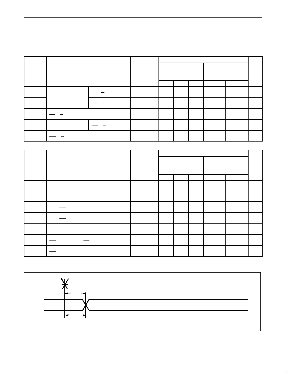
AC ELECTRICAL CHARACTERISTICS
LIMITS
T
amb
= +25
∞
C
T
amb
= 0
∞
C to +70
∞
C
SYMBOL
PARAMETER
TEST
V
CC
= +5.0V
V
CC
= +5.0V
±
10%
UNIT
CONDITION
C
L
= 50pF, R
L
= 500
C
L
= 50pF, R
L
= 500
MIN
TYP
MAX
MIN
MAX
t
PLH
t
PHL
Access time
Propagation delay
An to Qn
Waveform 1
2.5
2.0
5.0
4.5
8.0
8.0
2.5
2.0
8.0
8.0
ns
t
PZH
t
PZL
Enable time
CE to Qn
Waveform 2
2.0
2.0
3.5
4.0
6.0
7.0
1.5
2.0
7.0
7.5
ns
t
PHZ
t
PLZ
Disable time
CE to Qn
Waveform 3
2.5
1.5
4.5
3.0
7.0
5.5
2.0
1.5
8.0
6.0
ns
t
PZH
t
PZL
Write recovery time
Enable time
WE to Qn
Waveform 4
2.0
2.5
4.0
4.5
6.5
7.5
2.0
2.5
7.0
8.0
ns
t
PHZ
t
PLZ
Disable time
WE to Qn
Waveform 4
3.5
1.5
5.5
3.5
8.5
6.5
3.0
1.5
9.0
7.0
ns
AC SETUP REQUIREMENT
LIMITS
T
amb
= +25
∞
C
T
amb
= 0
∞
C to +70
∞
C
SYMBOL
PARAMETER
TEST
V
CC
= +5.0V
V
CC
= +5.0V
±
10%
UNIT
CONDITION
C
L
= 50pF, R
L
= 500
C
L
= 50pF, R
L
= 500
MIN
TYP
MAX
MIN
MAX
t
su
(H)
t
su
(L)
Setup time, high or low
An to WE
Waveform 4
4.5
4.5
5.0
5.0
ns
t
h
(H)
t
h
(L)
Hold time, high or low
An to WE
Waveform 4
0
0
0
0
ns
t
su
(H)
t
su
(L)
Setup time, high or low
Dn to WE
Waveform 4
7.5
6.5
9.0
8.0
ns
t
h
(H)
t
h
(L)
Hold time, high or low
Dn to WE
Waveform 4
0
0
0
0
ns
t
su
(L)
Setup time, low
CE (falling edge) to WE (falling edge)
Waveform 4
0
0
ns
t
h
(L)
Hold time, low
WE (falling edge) to WE (rising edge)
Waveform 4
6.5
7.5
ns
t
w
(L)
Pulse width, low
WE
Waveform 4
7.0
8.0
ns
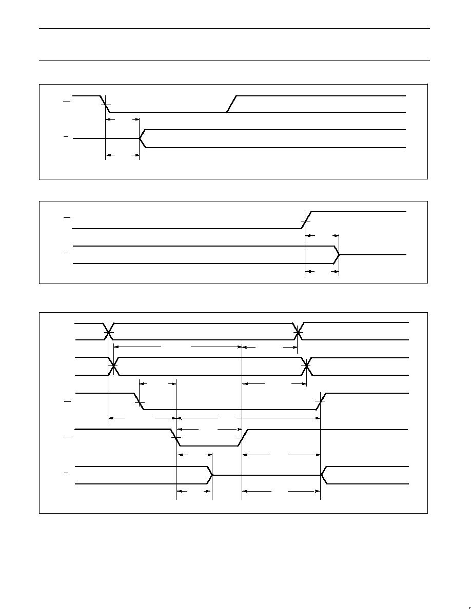
AC WAVEFORMS FOR READ CYCLES
VM
VM
Qn
An
tPHL
tPLH
NOTE:
For all waveforms, V
M
= 1.5V.
SF00303
Waveform 1. Read cycle, address access time
Philips Semiconductors
Product specification
74F189A
64-bit TTL bipolar RAM, inverting (3-State)
1990 Feb 23
6
VM
VM
Qn
CE
tPZH
tPZL
NOTE:
For all waveforms, V
M
= 1.5V.
SF00304
Waveform 2. Read cycle, chip enable access time
VM
VM
Qn
CE
tPHZ
tPLZ
NOTE:
For all waveforms, V
M
= 1.5V.
SF00305
Waveform 3. Read cycle, chip disable time
AC WAVEFORMS FOR WRITE CYCLE
VM
VM
An
tsu (H or L)
tPZH
VM
Qn
tPHZ
tPLZ
VM
VM
Dn
VM
CE
VM
VM
VM
WE
th (H or L)
VM
th (H or L)
tsu ( L)
tsu (H or L)
th ( L)
tw ( L)
VM
Hi≠Z
tPZL
NOTE:
For all waveforms, V
M
= 1.5V.
SF00306
Waveform 4. Write cycle
Philips Semiconductors
Product specification
74F189A
64-bit TTL bipolar RAM, inverting (3-State)
1990 Feb 23
7
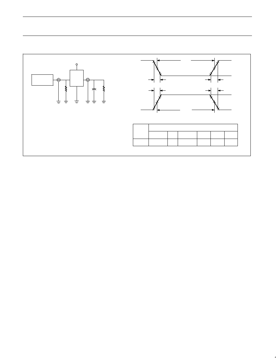
TEST CIRCUIT AND WAVEFORM
tw
90%
VM
10%
90%
VM
10%
90%
VM
10%
90%
VM
10%
NEGATIVE
PULSE
POSITIVE
PULSE
tw
AMP (V)
0V
0V
tTHL (tf
)
INPUT PULSE REQUIREMENTS
rep. rate
t
w
t
TLH
t
THL
1MHz
500ns
2.5ns
2.5ns
Input Pulse Definition
VCC
family
74F
D.U.T.
PULSE
GENERATOR
RL
CL
RT
VIN
VOUT
Test Circuit for Totem-Pole Outputs
DEFINITIONS:
R
L
= Load resistor;
see AC ELECTRICAL CHARACTERISTICS for value.
C
L
= Load capacitance includes jig and probe capacitance;
see AC ELECTRICAL CHARACTERISTICS for value.
R
T
= Termination resistance should be equal to Z
OUT
of
pulse generators.
tTHL (tf
)
tTLH (tr
)
tTLH (tr
)
AMP (V)
amplitude
3.0V
1.5V
V
M
SF00006
Philips Semiconductors
Product specification
74F189A
64-bit TTL bipolar RAM, inverting (3-State)
1990 Feb 23
8
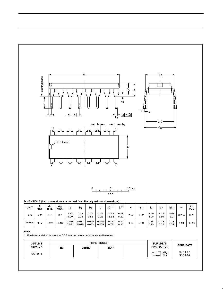
DIP16:
plastic dual in-line package; 16 leads (300 mil)
SOT38-4
Philips Semiconductors
Product specification
74F189A
64-bit TTL bipolar RAM, inverting (3-State)
1990 Feb 23
9
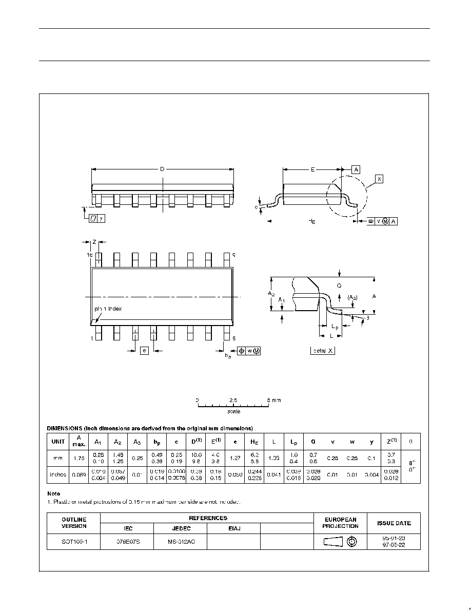
SO16:
plastic small outline package; 16 leads; body width 3.9 mm
SOT109-1
Philips Semiconductors
Product specification
74F189A
64-bit TTL bipolar RAM, inverting (3-State)
yyyy mmm dd
10
Definitions
Short-form specification -- The data in a short-form specification is extracted from a full data sheet with the same type number and title. For
detailed information see the relevant data sheet or data handbook.
Limiting values definition -- Limiting values given are in accordance with the Absolute Maximum Rating System (IEC 134). Stress above one
or more of the limiting values may cause permanent damage to the device. These are stress ratings only and operation of the device at these or
at any other conditions above those given in the Characteristics sections of the specification is not implied. Exposure to limiting values for extended
periods may affect device reliability.
Application information -- Applications that are described herein for any of these products are for illustrative purposes only. Philips
Semiconductors make no representation or warranty that such applications will be suitable for the specified use without further testing or
modification.
Disclaimers
Life support -- These products are not designed for use in life support appliances, devices or systems where malfunction of these products can
reasonably be expected to result in personal injury. Philips Semiconductors customers using or selling these products for use in such applications
do so at their own risk and agree to fully indemnify Philips Semiconductors for any damages resulting from such application.
Right to make changes -- Philips Semiconductors reserves the right to make changes, without notice, in the products, including circuits, standard
cells, and/or software, described or contained herein in order to improve design and/or performance. Philips Semiconductors assumes no
responsibility or liability for the use of any of these products, conveys no license or title under any patent, copyright, or mask work right to these
products, and makes no representations or warranties that these products are free from patent, copyright, or mask work right infringement, unless
otherwise specified.
Philips Semiconductors
811 East Arques Avenue
P.O. Box 3409
Sunnyvale, California 94088≠3409
Telephone 800-234-7381
©
Copyright Philips Electronics North America Corporation 1998
All rights reserved. Printed in U.S.A.
print code
Date of release: 10-98
Document order number:
9397-750-05092
Philips
Semiconductors
Data sheet
status
Objective
specification
Preliminary
specification
Product
specification
Product
status
Development
Qualification
Production
Definition
[1]
This data sheet contains the design target or goal specifications for product development.
Specification may change in any manner without notice.
This data sheet contains preliminary data, and supplementary data will be published at a later date.
Philips Semiconductors reserves the right to make chages at any time without notice in order to
improve design and supply the best possible product.
This data sheet contains final specifications. Philips Semiconductors reserves the right to make
changes at any time without notice in order to improve design and supply the best possible product.
Data sheet status
[1]
Please consult the most recently issued datasheet before initiating or completing a design.