 | –≠–ª–µ–∫—Ç—Ä–æ–Ω–Ω—ã–π –∫–æ–º–ø–æ–Ω–µ–Ω—Ç: N74F191D | –°–∫–∞—á–∞—Ç—å:  PDF PDF  ZIP ZIP |

Philips
Semiconductors
74F191
Up/down binary counter with reset and
ripple clock
Product specification
IC15 Data Handbook
1995 Jul 17
INTEGRATED CIRCUITS

Philips Semiconductors
Product specification
74F191
Up/Down binary counter with reset and ripple clock
2
1995 Jul 17
853≠0352 15459
FEATURES
∑
High speed ≠125MHz typical f
MAX
∑
Synchronous, reversible counting
∑
4-Bit binary
∑
Asynchronous parallel load capability
∑
Cascadable without external logic
∑
Single up/down control input
DESCRIPTION
The 74F191 is a 4-bit binary counter. It contains four edge-triggered
master/slave flip-flops with internal gating and steering logic to
provide asynchronous preset and synchronous count-up and
count-down operations.
Asynchronous parallel load capability permits the counter to be
preset to any desired number. Information present on the parallel
data inputs (D
0
- D
3
) is loaded into the counter and appears on the
outputs when the Parallel Load (PL) input is Low. This operation
overrides the counting function. Counting is inhibited by a High level
on the count enable (CE) input. When CE is Low, internal state
changes are initiated. Overflow/underflow indications are provided
by two types of outputs, the Terminal Count (TC) and Ripple Clock
(RC).
The TC output is normally Low and goes High when: 1) the count
reaches zero in the countdown mode or 2) reaches "15" in the count
up mode. The TC output will remain High until a state change
occurs, either by counting or presetting, or until U/D is changed. TC
output should not be used as a clock signal because it is subject to
decoding spikes. The TC signal is used internally to enable the RC
output. When TC is High and CE is Low, the RC follows the clock
pulse. The RC output essentially duplicates the Low clock pulse
width, although delayed in time by two gate delays.
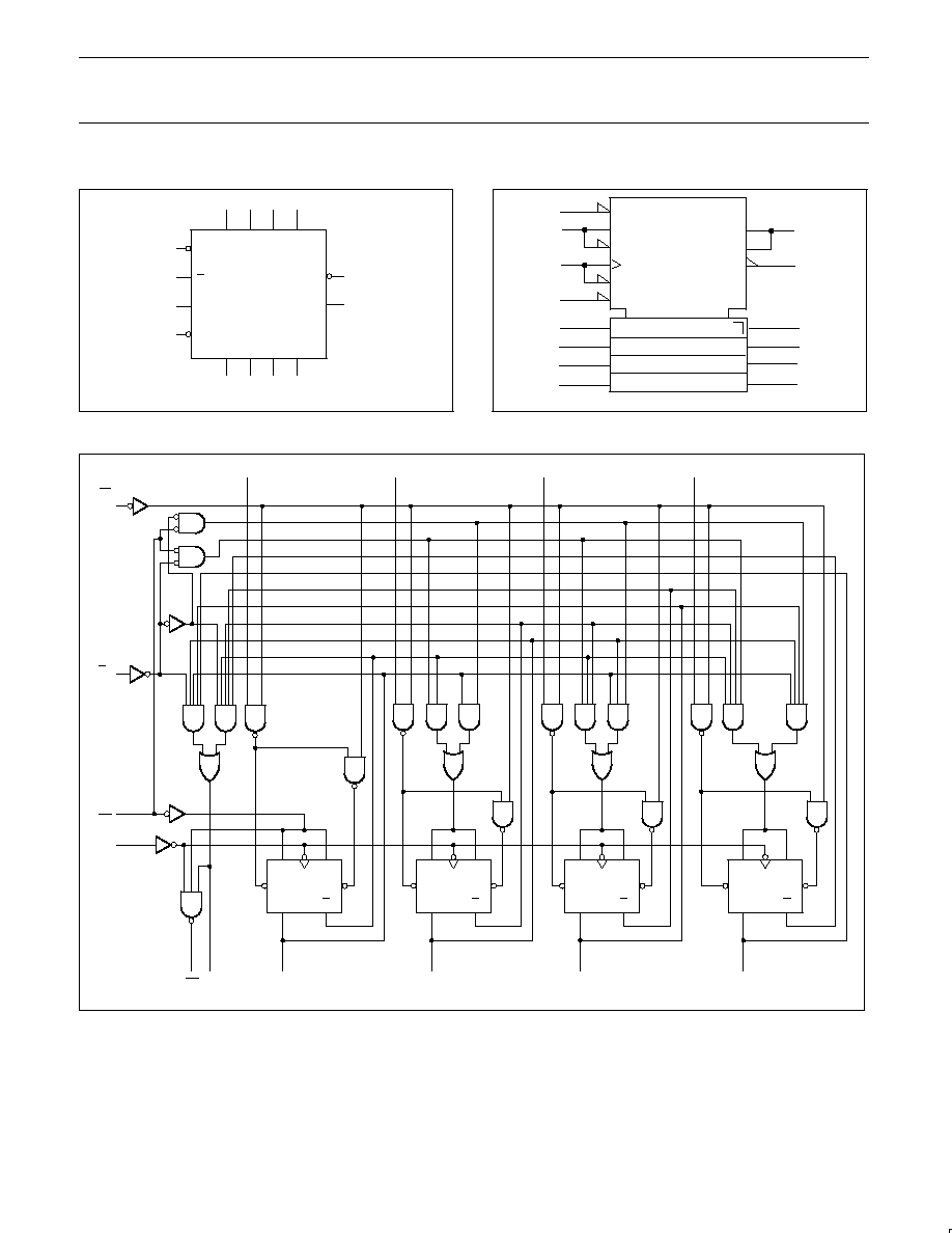
PIN CONFIGURATION
16
15
14
13
12
11
10
9
8
7
6
5
4
3
2
1
CE
Q0
D0
D1
Q1
D2
Q2
GND
CP
Q3
D3
VCC
U/D
RC
TC
PL
SF00729
TYPE
TYPICAL f
MAX
TYPICAL
SUPPLY CURRENT
(TOTAL)
74F191
125MHz
40mA
ORDERING INFORMATION
DESCRIPTION
COMMERCIAL RANGE
V
CC
= 5V
±
10%,
T
amb
= 0
∞
C to +70
∞
C
PKG DWG #
16-pin plastic DIP
N74F191N
SOT38-4
16-pin plastic SO
N74F191D
SOT109-1
INPUT AND OUTPUT LOADING AND FAN-OUT TABLE
PINS
DESCRIPTION
74F(U.L.)
HIGH/LOW
LOAD VALUE
HIGH/LOW
D
0
- D
3
Data inputs
1.0/1.0
20
µ
A/0.6mA
CE
Count enable input (active Low)
1.0/3.0
20
µ
A/1.8mA
CP
Clock pulse input (active rising edge)
1.0/1.0
20
µ
A/0.6mA
PL
Asynchronous parallel load control input (active Low)
1.0/1.0
20
µ
A/0.6mA
U/D
Up/down count control input
1.0/1.0
20
µ
A/0.6mA
Q
0
- Q
3
Flip-flop outputs
50/33
1.0mA/20mA
RC
Ripple clock output (active low)
50/33
1.0mA/20mA
TC
Terminal count output
50/33
1.0mA/20mA
NOTE: One (1.0) FAST Unit Load (U.L.) is defined as: 20
µ
A in the High state and 0.6mA in the Low state.
Philips Semiconductors
Product specification
74F191
Up/Down binary counter with reset and ripple clock
1995 Jul 17
3
LOGIC SYMBOL
15
1
10
9
7
6
2
3
14
5
CP
Q0
D0 D1
Q1
D2
Q2
Q3
D3
CE
U/D
TC
RC
4
12
13
PL
11
SF00730
V
CC
=Pin 16
GND=Pin 8
LOGIC SYMBOL (IEEE/IEC)
4
5
14
11
[1]
C5 [LOAD]
15
1
10
9
5D
3
2
6
7
1,2≠/1,3+
G4
EN1
SF00731
M2[DOWN]
M3[UP]
CTR DIV 10
6, 4, 1
[2]
[4]
[8]
+ ≠
12
13
2(CT=0)Z6
3(CT=15)Z6
LOGIC DIAGRAM
U/D
K
J
Q
CP
Q
S
D
R
D
K
J
Q
CP
Q
S
D
R
D
K
J
Q
CP
Q
S
D
R
D
K
J
Q
CP
Q
S
D
R
D
D
0
D
1
D
2
D
3
Q
1
Q
2
Q
3
Q
0
TC
RC
CP
CE
PL
15
1
10
9
7
6
2
3
12
13
14
4
5
11
V
CC
= Pin 16
GND = Pin 8
SF00732

Philips Semiconductors
Product specification
74F191
Up/Down binary counter with reset and ripple clock
1995 Jul 17
4
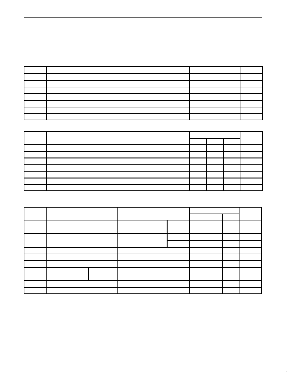
MODE SELECT -- FUNCTION TABLE
INPUTS
OUTPUTS
OPERATING MODE
PL
U/D
CE
CP
D
n
Q
n
L
L
X
X
X
X
X
X
L
H
L
H
Parallel load
H
L
l
X
Count up
Count up
H
H
l
X
Count down
Count down
H
X
H
X
X
No change
Hold (do nothing)
TC AND RC FUNCTION TABLE
INPUTS
TERMINAL COUNT STATE
OUTPUTS
U/D
CE
CP
Q
0
Q
1
Q
2
Q
3
TC
RC
H
H
X
H
H
H
H
L
H
L
H
X
H
H
H
H
H
H
L
L
H
H
H
H
H
L
H
X
L
L
L
L
L
H
H
H
X
L
L
L
L
H
H
H
L
L
L
L
L
H
H = High voltage level steady state
L = Low voltage level steady state
X = Don't care
= Low pulse
= Low-to-High clock transition
l
= Low voltage level one set-up time prior to the Low-to-High clock transition

Philips Semiconductors
Product specification
74F191
Up/Down binary counter with reset and ripple clock
1995 Jul 17
5
APPLICATIONS
U/D
CE
CP
U/D
CE
CP
U/D
CE
CP
U/D
CE
CP
U/D
CE
CP
U/D
CE
CP
U/D
CE
CP
U/D
CE
CP
U/D
CE
CP
TC
TC
TC
RC
RC
RC
RC
RC
RC
DIRECTION CONTROL
CLOCK
ENABLE
ENABLE
DIRECTION CONTROL
CLOCK
ENABLE
DIRECTION CONTROL
CLOCK
a. N-Stage Counter Using Ripple Clock
b. Synchronous N-Stage Counter with Common Clock Using Ripple/Clock
c. Synchronous N-Stage Counter with Common Clock and Terminal Count
* = Carry Gate
*
*
SF00733
Figure 1.
The 74F191 simplifies the design of multi-stage counters, as
indicated in Figure 1, each RC output is used as the clock input for
the next higher stage. When the clock source has a limited drive
capability this configuration is particularly advantageous, since the
clock source drives only the first stage. It is only necessary to inhibit
the first stage to prevent counting in all stages, since a High signal
on CE inhibits the RC output pulse as indicated in the Mode Select
Table. The timing skew between state changes in the first and last
stages is represented by the cumulative delay of the clock as it
ripples through the preceding stages. This is a disadvantage of the
configuration in some applications.
Figure 1b shows a method of causing state changes to occur
simultaneously in all stages. The RC output signals propagate in
ripple fashion and all clock inputs are driven in parallel. The Low
state duration of the clock in this configuration must be long enough
to allow the negative-going edge of the RC signal to ripple through
to the last stage before the clock goes High. Since the RC output of
any package goes High shortly after its clock input goes High, there
is no such restriction on the High state duration of the clock.
In Figure 1c, the configuration shown avoids ripple delays and their
associated restrictions. The combined TC signals from all the
preceding stages forms the CE input signal for a given stage. An
enable signal must also be included in each carry gate in order to
inhibit counting. The TC output of a given stage is not affected by its
own CE, therefore, the simple inhibit scheme of Figure 1a and 1b
does not apply.
Philips Semiconductors
Product specification
74F191
Up/Down binary counter with reset and ripple clock
1995 Jul 17
6
ABSOLUTE MAXIMUM RATINGS
(Operation beyond the limits set forth in this table may impair the useful life of the device.
Unless otherwise noted these limits are over the operating free-air temperature range.)
SYMBOL
PARAMETER
RATING
UNIT
V
CC
Supply voltage
≠0.5 to +7.0
V
V
IN
Input voltage
≠0.5 to +7.0
V
I
IN
Input current
≠30 to +5.0
mA
V
OUT
Voltage applied to output in High output state
≠0.5 to +V
CC
V
I
OUT
Current applied to output in Low output state
40
mA
T
amb
Operating free-air temperature range
0 to +70
o
C
T
stg
Storage temperature
≠65 to +150
o
C
RECOMMENDED OPERATING CONDITIONS
SYMBOL
PARAMETER
LIMITS
UNIT
SYMBOL
PARAMETER
Min
Nom
Max
UNIT
V
CC
Supply voltage
4.5
5.0
5.5
V
V
IH
High-level input voltage
2.0
V
V
IL
Low-level input voltage
0.8
V
I
IK
Input clamp current
≠18
mA
I
OH
High-level output current
≠1
mA
I
OL
Low-level output current
20
mA
T
amb
Operating free-air temperature range
0
70
o
C
DC ELECTRICAL CHARACTERISTICS
(Over recommended operating free-air temperature range unless otherwise noted.)
SYMBOL
PARAMETER
TEST CONDITIONS
1
LIMITS
UNIT
SYMBOL
PARAMETER
TEST CONDITIONS
1
Min
Typ
2
Max
UNIT
V
O
High level output voltage
V
CC
= Min, V
IL
= Max,
±
10%V
CC
2.5
V
V
OH
High-level output voltage
V
CC
Min, V
IL
Max,
I
OH
= Max, V
IH
= Min
±
5%V
CC
2.7
3.4
V
V
O
Low level output voltage
V
CC
= Min, V
IL
= Max,
±
10%V
CC
0.30
0.50
V
V
OL
Low-level output voltage
V
CC
Min, V
IL
Max,
I
OL
= Max, V
IH
= Min
±
5%V
CC
0.30
0.50
V
V
IK
Input clamp voltage
V
CC
= Min, I
I
= I
IK
≠0.73
≠1.2
V
I
I
Input current at maximum input voltage
V
CC
= Max, V
I
= 7.0V
100
µ
A
I
IH
High-level input current
V
CC
= Max, V
I
= 2.7V
20
µ
A
I
IL
Low-level input current
CE
V
CC
= Max V = 0 5V
≠1.8
mA
Others
V
CC
= Max, V
I
= 0.5V
≠0.6
mA
I
OS
Short-circuit output current
3
V
CC
= Max
≠60
≠150
mA
I
CC
Supply current
4
(total)
V
CC
= Max
40
55
mA
NOTES:
1. For conditions shown as MIN or MAX, use the appropriate value specified under recommended operating conditions for the applicable type.
2. All typical values are at V
CC
= 5V, T
amb
= 25
∞
C.
3. Not more than one output should be shorted at a time. For testing I
OS
, the use of high-speed test apparatus and/or sample-and-hold
techniques are preferable in order to minimize internal heating and more accurately reflect operational values. Otherwise, prolonged shorting
of a High output may raise the chip temperature well above normal and thereby cause invalid readings in other parameter tests. In any
sequence of parameter tests, I
OS
tests should be performed last.
4. Measure I
CC
all inputs grounded and all outputs open.

Philips Semiconductors
Product specification
74F191
Up/Down binary counter with reset and ripple clock
1995 Jul 17
7
AC ELECTRICAL CHARACTERISTICS
LIMITS
T
amb
= +25
∞
C
T
amb
= 0
∞
C to +70
∞
C
SYMBOL
PARAMETER
TEST CONDITIONS
V
CC
= +5.0V
V
CC
= +5.0V
±
10%
UNIT
C
L
= 50pF, R
L
= 500
C
L
= 50pF, R
L
= 500
Min
Typ
Max
Min
Max
f
MAX
Maximum clock frequency
to Qn outputs
Waveform 1
100
125
90
MHz
f
MAX
Maximum clock frequency
to RC outputs
Waveform 1
85
95
75
MHz
t
PLH
t
PHL
Propagation delay
CP to Q
n
Waveform 1
2.5
5.0
4.5
7.5
8.0
11.5
2.0
5.0
8.5
12.0
ns
ns
t
PLH
t
PHL
Propagation delay
CP to TC
Waveform 1
6.5
6.0
9.0
8.0
12.5
11.0
6.0
6.0
13.0
12.0
ns
ns
t
PLH
t
PHL
Propagation delay
CP to RC
Waveform 2
2.5
3.0
4.5
5.0
7.5
7.5
2.0
2.5
8.0
8.0
ns
ns
t
PLH
t
PHL
Propagation delay
CE to RC
Waveform 2
2.0
3.0
4.0
5.0
7.0
7.5
2.0
3.0
7.5
8.0
ns
ns
t
PLH
t
PHL
Propagation delay
U/D to RC
Waveform 2
8.0
4.5
11.0
7.5
16.0
10.5
8.0
4.0
17.0
11.0
ns
ns
t
PLH
t
PHL
Propagation delay
U/D to TC
Waveform 4
4.0
3.0
6.5
6.0
9.5
9.5
3.0
3.0
10.5
10.0
ns
ns
t
PLH
t
PHL
Propagation delay
D
n
to Q
n
Waveform 3
2.0
6.5
4.0
9.0
7.0
12.0
1.5
6.5
7.5
13.0
ns
ns
t
PLH
t
PHL
Propagation delay
D
n
to TC
Waveform 3
Waveform 4
5.5
6.5
9.5
9.5
13.0
13.0
5.0
6.0
14.0
14.0
ns
ns
t
PLH
t
PHL
Propagation delay
D
n
to RC
Waveform 3
Waveform 4
6.0
6.0
14.0
11.0
18.0
13.5
6.0
6.0
19.5
15.0
ns
ns
t
PLH
t
PHL
Propagation delay
PL to Q
n
Waveform 5
4.5
5.5
6.5
8.0
9.5
11.5
4.0
5.0
10.5
12.0
ns
ns
t
PLH
t
PHL
Propagation delay
PL to TC
Waveform 5
5.5
6.0
8.5
10.5
12.0
13.5
5.5
6.0
13.0
14.5
ns
ns
t
PLH
t
PHL
Propagation delay
PL to RC
Waveform 5
8.5
7.5
16.0
10.0
18.5
13.0
8.5
7.0
21.0
13.5
ns
ns

Philips Semiconductors
Product specification
74F191
Up/Down binary counter with reset and ripple clock
1995 Jul 17
8
AC SETUP REQUIREMENTS
LIMITS
T
amb
= +25
∞
C
T
amb
= 0
∞
C to +70
∞
C
SYMBOL
PARAMETER
TEST CONDITIONS
V
CC
= +5.0V
V
CC
= +5.0V
±
10%
UNIT
C
L
= 50pF, R
L
= 500
C
L
= 50pF, R
L
= 500
Min
Typ
Max
Min
Max
t
s
(H)
t
s
(L)
Setup time, High or Low
D
n
to PL
Waveform 6
4.5
4.5
5.0
5.0
ns
ns
t
h
(H)
t
h
(L)
Hold time, High or Low
D
n
to PL
Waveform 6
2.0
2.0
2.0
2.0
ns
ns
t
s
(L)
Setup time, Low CE
to
CP
Waveform 6
10.0
10.0
ns
t
h
(L)
Hold time, Low CE to CP
Waveform 6
0
0
ns
t
s
(H)
t
s
(L)
Setup time, High or Low
U/D to CP
Waveform 6
12.0
12.0
12.0
12.0
ns
ns
t
h
(H)
t
h
(L)
Hold time, High or Low
U/D to CP
Waveform 6
0
0
0
0
ns
ns
t
w
(H)
t
w
(L)
CP Pulse width, High or Low
Waveform 1
3.5
6.0
3.5
6.0
ns
ns
t
w
(L)
PL Pulse width, Low
Waveform 5
6.0
6.0
ns
t
rec
Recovery time, PL to CP
Waveform 5
6.0
6.0
ns
Philips Semiconductors
Product specification
74F191
Up/Down binary counter with reset and ripple clock
1995 Jul 17
9
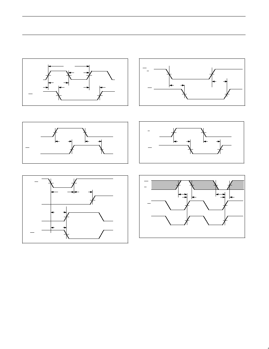
AC WAVEFORMS
NOTE: For all waveforms, V
M
= 1.5V
V
M
t
PLH
t
PHL
V
M
V
M
V
M
CP
RC, Q
n
, TC
1/f
MAX
t
W
(H)
t
W
(L)
SF00734
Waveform 1. Propagation Delay, Clock Input to Output,
Clock Pulse Width, and Maximum Clock Frequency.
V
M
V
M
V
M
V
M
t
PHL
t
PLH
D
n
RC, TC, Q
n
SF00736
Waveform 3. Propagation Delay, Non-Inverting Path
V
M
V
M
V
M
t
W
(L)
t
REC
V
M
TC, Q
n
CP
PL
V
M
RC, Q
n
t
PLH
SF00738
t
PHL
Waveform 5. Parallel Load Pulse Width, Parallel Load to Output
Delay and Parallel Load to Clock Recovery Time
t
PLH
CE, CP
U/D
RC
V
M
V
M
V
M
V
M
SF00735
t
PHL
Waveform 2. Propagation Delay, Clock, Clock Enable or
Up/Down to Ripple Clock Output
V
M
V
M
V
M
V
M
t
PHL
t
PLH
U/D, D
n
RC, TC
SF00737
Waveform 4. Propagation Delay, Inverting Path
The shaded areas indicate when the input is permitted
to change for predictable output performance.
V
M
V
M
PL
t
S
(H)
t
h
(H)
t
S
(L)
t
h
(L)
V
M
CP
SF00739
V
M
V
M
CE,
D
n
U/D
Waveform 6. Data Set Up and Hold Times

Philips Semiconductors
Product specification
74F191
Up/Down binary counter with reset and ripple clock
1995 Jul 17
10
TEST CIRCUIT AND WAVEFORM
tw
90%
VM
10%
90%
VM
10%
90%
VM
10%
90%
VM
10%
NEGATIVE
PULSE
POSITIVE
PULSE
tw
AMP (V)
0V
0V
tTHL (tf
)
INPUT PULSE REQUIREMENTS
rep. rate
t
w
t
TLH
t
THL
1MHz
500ns
2.5ns
2.5ns
Input Pulse Definition
VCC
family
74F
D.U.T.
PULSE
GENERATOR
RL
CL
RT
VIN
VOUT
Test Circuit for Totem-Pole Outputs
DEFINITIONS:
R
L
= Load resistor;
see AC ELECTRICAL CHARACTERISTICS for value.
C
L
= Load capacitance includes jig and probe capacitance;
see AC ELECTRICAL CHARACTERISTICS for value.
R
T
= Termination resistance should be equal to Z
OUT
of
pulse generators.
tTHL (tf
)
tTLH (tr
)
tTLH (tr
)
AMP (V)
amplitude
3.0V
1.5V
V
M
SF00006
Philips Semiconductors
Product specification
74F191
Up/down binary counter with reset and ripple clock
1995 Jul 17
11
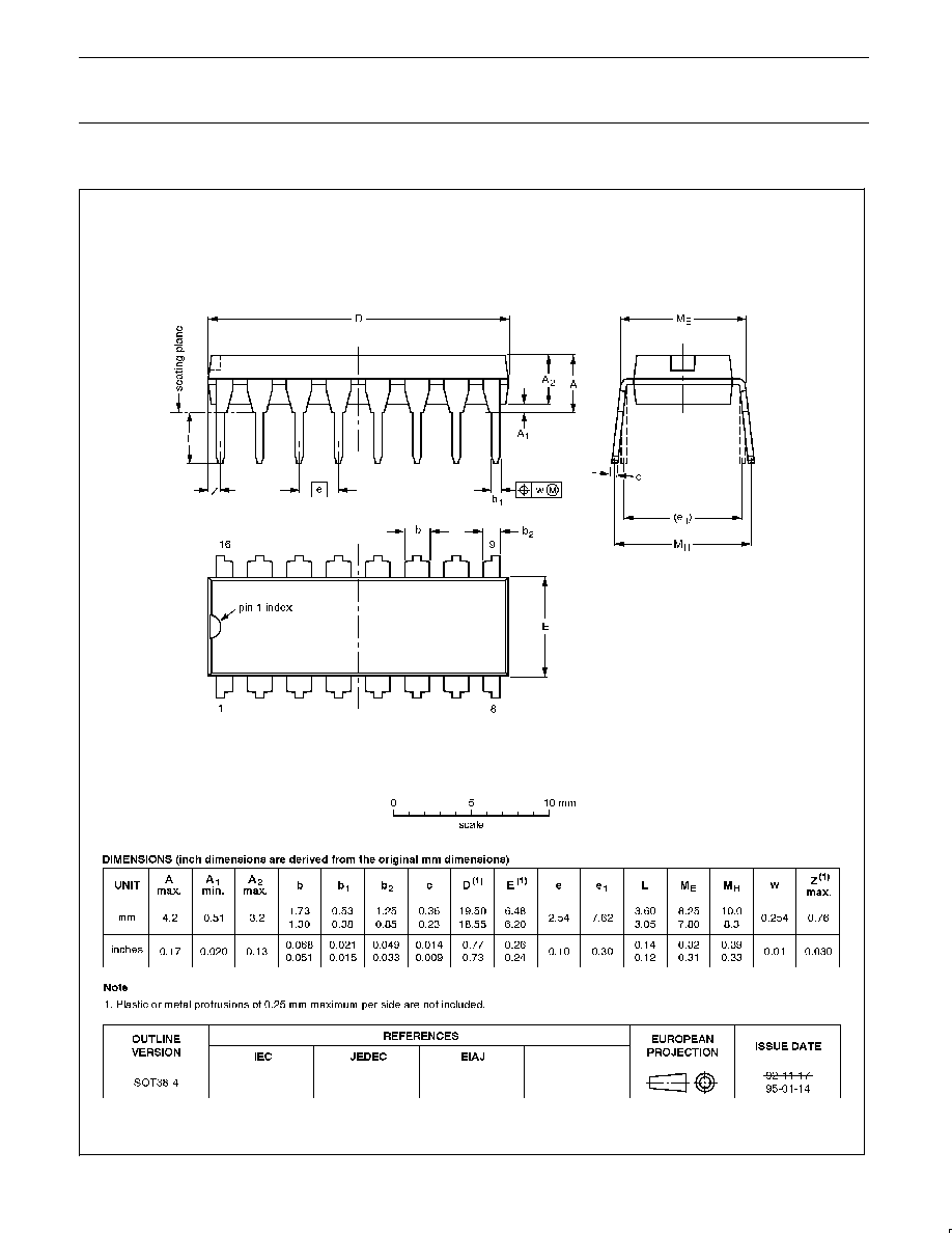
DIP16:
plastic dual in-line package; 16 leads (300 mil)
SOT38-4
Philips Semiconductors
Product specification
74F191
Up/down binary counter with reset and ripple clock
1995 Jul 17
12
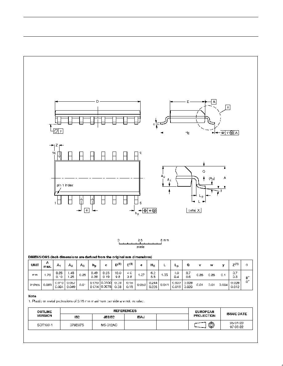
SO16:
plastic small outline package; 16 leads; body width 3.9 mm
SOT109-1

Philips Semiconductors
Product specification
74F191
Up/down binary counter with reset and ripple clock
1995 Jul 17
13
NOTES
Philips Semiconductors
Product specification
74F191
Up/down binary counter with reset and ripple clock
yyyy mmm dd
14
Definitions
Short-form specification -- The data in a short-form specification is extracted from a full data sheet with the same type number and title. For
detailed information see the relevant data sheet or data handbook.
Limiting values definition -- Limiting values given are in accordance with the Absolute Maximum Rating System (IEC 134). Stress above one
or more of the limiting values may cause permanent damage to the device. These are stress ratings only and operation of the device at these or
at any other conditions above those given in the Characteristics sections of the specification is not implied. Exposure to limiting values for extended
periods may affect device reliability.
Application information -- Applications that are described herein for any of these products are for illustrative purposes only. Philips
Semiconductors make no representation or warranty that such applications will be suitable for the specified use without further testing or
modification.
Disclaimers
Life support -- These products are not designed for use in life support appliances, devices or systems where malfunction of these products can
reasonably be expected to result in personal injury. Philips Semiconductors customers using or selling these products for use in such applications
do so at their own risk and agree to fully indemnify Philips Semiconductors for any damages resulting from such application.
Right to make changes -- Philips Semiconductors reserves the right to make changes, without notice, in the products, including circuits, standard
cells, and/or software, described or contained herein in order to improve design and/or performance. Philips Semiconductors assumes no
responsibility or liability for the use of any of these products, conveys no license or title under any patent, copyright, or mask work right to these
products, and makes no representations or warranties that these products are free from patent, copyright, or mask work right infringement, unless
otherwise specified.
Philips Semiconductors
811 East Arques Avenue
P.O. Box 3409
Sunnyvale, California 94088≠3409
Telephone 800-234-7381
©
Copyright Philips Electronics North America Corporation 1998
All rights reserved. Printed in U.S.A.
print code
Date of release: 10-98
Document order number:
9397-750-05093
Philips
Semiconductors
Data sheet
status
Objective
specification
Preliminary
specification
Product
specification
Product
status
Development
Qualification
Production
Definition
[1]
This data sheet contains the design target or goal specifications for product development.
Specification may change in any manner without notice.
This data sheet contains preliminary data, and supplementary data will be published at a later date.
Philips Semiconductors reserves the right to make chages at any time without notice in order to
improve design and supply the best possible product.
This data sheet contains final specifications. Philips Semiconductors reserves the right to make
changes at any time without notice in order to improve design and supply the best possible product.
Data sheet status
[1]
Please consult the most recently issued datasheet before initiating or completing a design.