Philips Semiconductors FAST Products
Preliminary specification
74F224
16
◊
4 Synchronous FIFO (3-State)
1
September 7, 1990
FEATURES
∑
Independent synchronous inputs and
outputs
∑
Organized as 16 words of 4 bits
∑
DC to 50MHz data rate
∑
3-State outputs
∑
Cascadable in word≠width and depth
direction
DESCRIPTION
This 64-bit active element First-In-First-Out
(FIFO) is a monolithic Schottky-clamped
transistor-transistor logic (STLL) array
organized as 16 words of 4-bits each. A
memory system using the 74F224 can be
easily expanded in multiples of 15m+1 words
or of 4n bits, or both (where n is the number
of packages in the horizontal array).
However, an external gating is required (see
Figure 1). For longer words using 74F224,
the IR signals of the first-rank packages and
OR signals of the last-rank packages must be
ANDed for proper synchronization.The
3-State outputs controlled by a single input
(OE) make bus connection and multiplexing
easy.
TYPE
TYPICAL
f
max
TYPICAL
SUPPLY
CURRENT
(TOTAL)
74F224
50MHz
90mA
ORDERING INFORMATION
ORDER CODE
DESCRIPTION
COMMERCIAL RANGE
DRAWING NUMBER
V
CC
= 5V
±
10%, T
amb
= 0
∞
C to +70
∞
C
16-pin plastic Dual In-line Package
N74F224N
0406C
16-pin plastic Small Outline Large
N74F224D
0171B
INPUT AND OUTPUT LOADING AND FAN OUT TABLE
PINS
DESCRIPTION
74F (U.L.)
HIGH/LOW
LOAD VALUE
HIGH/LOW
LDCP
Load clock input
1.0/1.0
20
µ
A
/
0.6mA
D0 ≠ D3
Data inputs
1.0/1.0
20
µ
A
/
0.6mA
OE
Output enable input (active high)
1.0/1.0
20
µ
A
/
0.6mA
UNCP
Unload clock input
1.0/1.0
20
µ
A
/
0.6mA
MR
Master reset input (active low)
1.0/1.0
20
µ
A
/
0.6mA
IR
Input ready output
50/33
1.0mA/20mA
Q0 ≠ Q3
Data outputs
50/33
1.0mA/20mA
OR
Output ready output
50/33
1.0mA/20mA
NOTE TO INPUT AND OUTPUT LOADING AND FAN OUT TABLE
1. One (1.0) FAST unit load is defined as: 20
µ
A in the high state and 0.6mA in the low state.
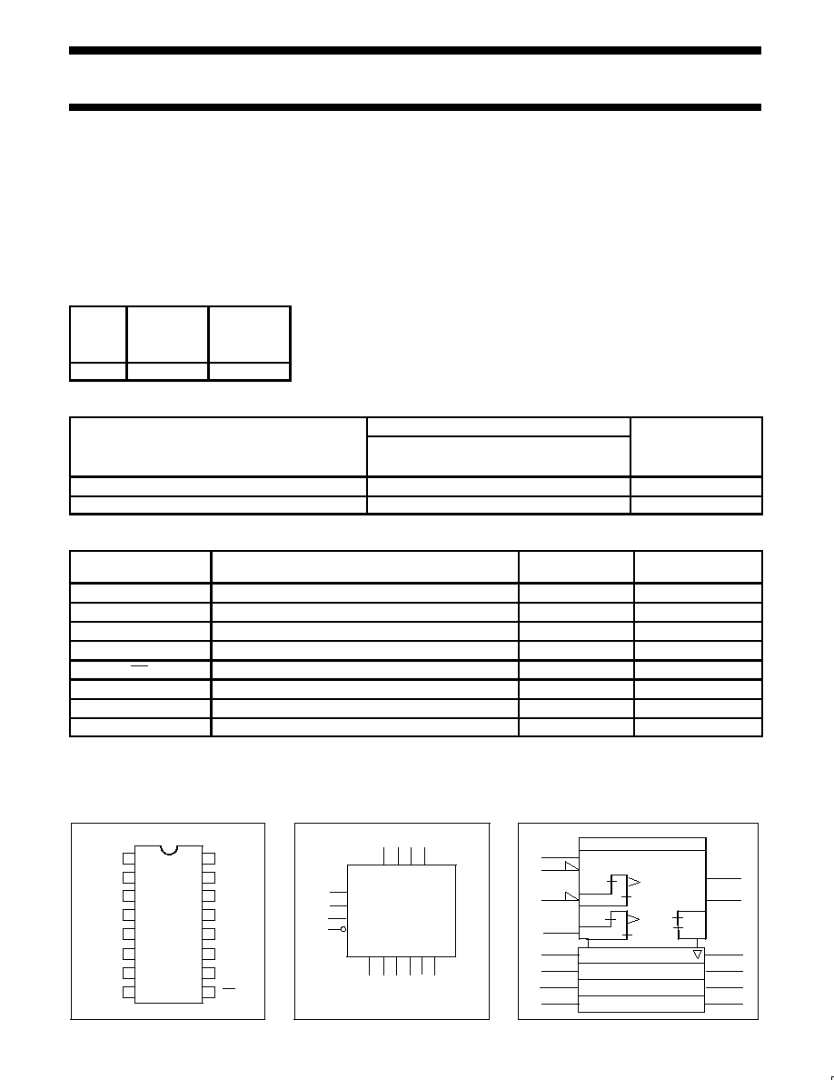
PIN CONFIGURATION
LOGIC SYMBOL
IED/IEEE SYMBOL
OE
IR
D0
D1
D3
VCC
LDCP
D2
GND
UNCP
OR
Q0
Q1
Q2
Q3
MR
Q0 Q1 Q2 Q3 IR OR
VCC
= Pin 16
GND
= Pin 8
D0 D1 D2 D3
OE
UNCP
LDCP
MR
1
13
3
9
4 5 6 7
13 12 11 10 2 14
1
9
7
10
6
13
5
12
4
13
1D
4,5
&
15
&
CT>0
V4
CT=0
2
2
Z3
≠
+/C1
CTR
CT<0
CT=0
EN5
FIFO 16 X 4
16
15
14
13
12
11
10
7
6
5
4
3
2
1
9
8
3
Z2
&
3
14
2