 | –≠–ª–µ–∫—Ç—Ä–æ–Ω–Ω—ã–π –∫–æ–º–ø–æ–Ω–µ–Ω—Ç: N74F225D | –°–∫–∞—á–∞—Ç—å:  PDF PDF  ZIP ZIP |
Document Outline
- FEATURES
- DESCRIPTION
- ORDERING INFORMATION
- INPUT AND OUTPUT LOADING AND FAN OUT TABLE
- RESET MODE
- WRITE MODE
- READ MODE
- PIN CONFIGURATION
- IEC/IEEE SYMBOL
- LOGIC SYMBOL
- LOGIC DIAGRAM
- ABSOLUTE MAXIMUM RATINGS
- RECOMMENDED OPERATING CONDITIONS
- DC ELECTRICAL CHARACTERISTICS
- AC ELECTRICAL CHARACTERISTICS
- AC SETUP REQUIREMENTS
- TYPICAL TIMING DIAGRAM
- AC WAVEFORMS
- APPLICATION
- TEST CIRCUIT AND WAVEFORM
- PACKAGE OUTLINES
- Data sheet status
- Definitions
- Disclaimers

Philips
Semiconductors
74F225
16X5 asynchronous FIFO (3-State)
Product specification
IC15 Data Handbook
1992 Jun 15
INTEGRATED CIRCUITS
Philips Semiconductors
Product specification
74F225
16
◊
5 asynchronous FIFO (3-State)
2
June 15, 1992
853-1652 06992
FEATURES
∑
Independent synchronous inputs and outputs
∑
Organized as 16 words of 5 bits
∑
DC to 25MHz data rate
∑
3≠State outputs
∑
Cascadable in word≠width and depth direction
DESCRIPTION
This 80≠bit active element First≠In≠First≠Out (FIFO) is a monolithic
Schottky≠clamped transistor≠transistor logic (STTL) array organized
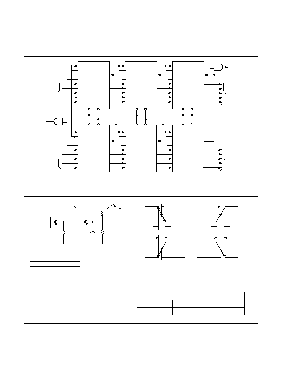
as 16≠words of 5≠bits each. A memory system using the 'F225 can
be easily expanded in multiples of 16≠words of 5≠bits as shown in
Figure 1. The 3≠State outputs controlled by a single enable input
(OE) make bus connection and multiplexing simple. The 'F225
processes data in a parallel format at any desired clock rate from
DC to 25MHz. Status of the 'F225 is provided by three outputs, Input
Ready (IR), Unload Clock Output (UNCPOUT) and Output Ready
(OR). The data outputs are non≠inverting with respect to the data
inputs and are disabled when the OE input is High. When OE is
Low, the data outputs are enabled to function as totem≠pole outputs.
TYPE
TYPICAL f
MAX
TYPICAL SUPPLY
CURRENT
( TOTAL)
74F225
25MHz
65mA
ORDERING INFORMATION
ORDER CODE
DESCRIPTION
COMMERCIAL RANGE
V
CC
= 5V
±
10%,
T
amb
= 0
∞
C to +70
∞
C
PKG DWG #
20≠pin plastic DIP
N74F225N
SOT146-1
20≠pin plastic SOL
N74F225D
SOT163-1
INPUT AND OUTPUT LOADING AND FAN OUT TABLE
PINS
DESCRIPTION
74F (U.L.)
HIGH/LOW
LOAD VALUE
HIGH/LOW
CPA, CPB
Load clock A and load clock B inputs
1.0/0.033
20
µ
A/20
µ
A
D0 ≠ D4
Data inputs
1.0/0.033
20
µ
A/20
µ
A
OE
Output enable input (active≠Low)
1.0/0.033
20
µ
A/20
µ
A
UNCPIN
Unload clock input
1.0/0.033
20
µ
A/20
µ
A
MR
Master reset input (active≠Low)
1.0/0.033
20
µ
A/20
µ
A
IR
Input ready output
50/33
1.0mA/20mA
UNCPOUT
Unload clock output (active≠Low)
50/33
1.0mA/20mA
Q0 ≠ Q4
Data outputs
150/40
3.0mA/24mA
OR
Output ready output
50/33
1.0mA/20mA
NOTE: One (1.0) FAST unit load is defined as: 20
µ
A in the High state and 0.6mA in the Low state.
RESET MODE
A High≠to≠Low transition on the Master Reset (MR) input invalidates
all data stored in the FIFO by clearing the control logic and setting
OR Low. This High≠to≠Low transition on the MR input does not
effect the data outputs but since OR is driven Low, it signifies invalid
data on the outputs.
WRITE MODE
Data may be written into the array on the Low≠to≠High transition of
either load clock (CPA or CPB) input. When writing data into the
FIFO, one of the load clock inputs must be held High while the other
strobes data into the FIFO. This arrangement allows either load
clock to function as an inhibit for the other. Input Ready (IR)
monitors the status of the last word location and signifies when the
FIFO is full. This output is High whenever the FIFO is available to
accept new data. The unload clock output (UNCPOUT) also
monitors the last word location. This output generates a
Low≠logic≠level pulse (synchronized to the internal clock pulse)
when the last word location is vacant
READ MODE
The Output Ready (OR) output is High when valid data is present on
the data outputs. Data in the array is shifted on the Low≠to≠High
transition of the Unload Clock Input (UNCPIN). In order for Output
Ready (OR) to go High, Unload Clock Input (UNCPIN) must also be
High.
Philips Semiconductors
Product specification
74F225
16
◊
5 asynchronous FIFO (3-State)
June 15, 1992
3
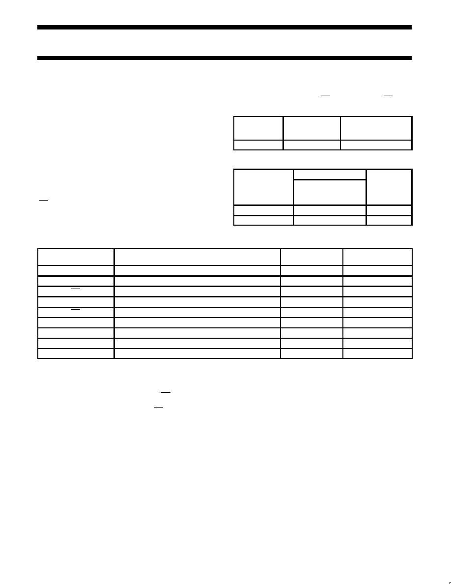
PIN CONFIGURATION
1
2
3
4
5
6
7
8
9
10
11
12
13
14
15
16
17
18
19
20
CPA
IR
D0
D1
GND
D3
OE
VCC
UNCPOUT
D2
D4
CPB
MR
OR
UNCPIN
Q0
Q1
Q2
Q3
Q4
SF00334
LOGIC SYMBOL
Q0 Q1 Q2 Q3 Q4 IR OR
VCC = Pin 20
GND
= Pin 10
D0 D1 D2 D3 D4
UNCPOUT
CPA
CPB
UNCPIN
OE
MR
1
19
16
9
18
4 5 6 7 8
15 14 13 12 11 2 17
3
SF00335
IEC/IEEE SYMBOL
9
18
7
12
6
13
5
14
4
15
1
1D
5
&
19
16
&
G1
CT>0
4
8
11
2CT<16
17
2
3
3
Z4
≠
+
G2/Z3
CTR
CT<16
CT=0
EN5
FIFO 16 X
5
1
SF00336
Philips Semiconductors
Product specification
74F225
16
◊
5 asynchronous FIFO (3-State)
June 15, 1992
4
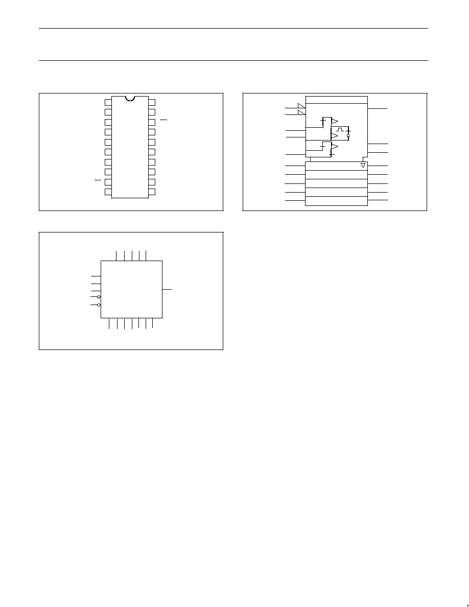
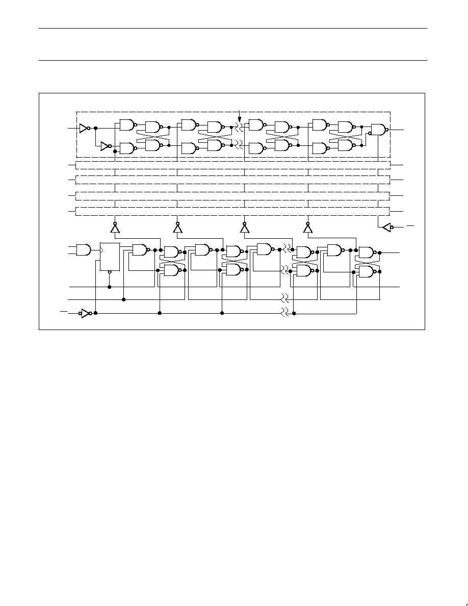
LOGIC DIAGRAM
14
13
12
11
9
VCC
=
pin 20
GND = pin 10
15
4
5
6
7
8
Detail A
Detail A
Detail A
Detail A
Detail A
CP
Q
D
CLR
D0
D1
D2
D3
D4
CPA
CPB
UNC-
POUT
Q1
Q2
Q3
Q4
QO
OE
Word 16
(last word)
Word 15
Word 2
Word 1
(first word)
Word 3≠14
same as 2 or 16
OR
UNCPIN
17
16
1
19
3
2
18
IR
MR
SF00337

Philips Semiconductors
Product specification
74F225
16
◊
5 asynchronous FIFO (3-State)
June 15, 1992
5
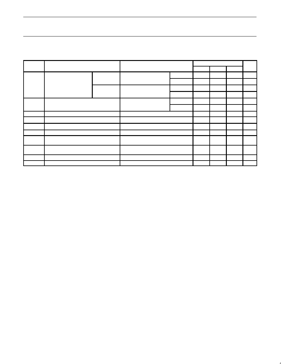
ABSOLUTE MAXIMUM RATINGS
(Operation beyond the limit set forth in this table may impair the useful life of the device. Unless otherwise noted these limits are over the
operating free air temperature range.)
SYMBOL
PARAMETER
RATING
UNIT
V
CC
Supply voltage
≠0.5 to +7.0
V
V
IN
Input voltage
≠0.5 to +7.0
V
I
IN
Input current
≠30 to +5
mA
V
OUT
Voltage applied to output in High output state
≠0.5 to V
CC
V
I
OUT
Current applied to output in Low output state
IR, OR, UNCPOUT
40
mA
Current applied to output in Low output state
Data outputs
48
mA
T
amb
Operating free air temperature range
0 to +70
∞
C
T
stg
Storage temperature range
≠65 to +150
∞
C
RECOMMENDED OPERATING CONDITIONS
SYMBOL
PARAMETER
LIMITS
UNIT
MIN
NOM
MAX
V
CC
Supply voltage
4.5
5.0
5.5
V
V
IN
High≠level input voltage
2.0
V
V
IL
Low≠level input voltage
0.8
V
I
Ik
Input clamp current
≠18
mA
I
OH
High≠level output current
IR, OR, UNCPOUT
≠1
mA
Data outputs
≠3
mA
I
OL
Low≠level output current
IR, OR, UNCPOUT
20
mA
Data outputs
24
mA
T
amb
Operating free air temperature range
0
+70
∞
C
Philips Semiconductors
Product specification
74F225
16
◊
5 asynchronous FIFO (3-State)
June 15, 1992
6
DC ELECTRICAL CHARACTERISTICS
(Over recommended operating free-air temperature range unless otherwise noted.)
SYMBOL
PARAMETER
TEST CONDITIONS
1
LIMITS
UNIT
MIN
TYP
2
MAX
IR, OR,
V
CC
= MIN, V
IL
= MAX
±
10%V
CC
2.5
V
V
OH
High-level output voltage
UNCPOUT
V
IH
= MIN, I
OH
= MAX
±
5%V
CC
2.7
V
Data
V
CC
= MIN, V
IL
= MAX
±
10%V
CC
2.4
V
outputs
V
IH
= MIN, I
OH
= MAX
±
5%V
CC
2.7
V
V
OL
Low-level output voltage
V
CC
= MIN, V
IL
= MAX
±
10%V
CC
0.35
0.50
V
V
IH
= MIN, I
OL
= MAX
±
5%V
CC
0.35
0.50
V
V
IK
Input clamp voltage
V
CC
= MIN, I
I
= I
IK
-0.73
-1.2
V
I
I
Input current at maximum input voltage
V
CC
= MAX, V
I
= 7.0V
100
µ
A
I
IH
High≠level input current
V
CC
= MAX, V
I
= 2.7V
20
µ
A
I
IL
Low≠level input current
V
CC
= MAX, V
I
= 0.5V
≠20
µ
A
I
OZH
Offset≠output current,
High≠level voltage applied
V
CC
= MAX, V
I
= 2.7V
50
µ
A
I
OZL
Offset≠output current,
Low≠level voltage applied
V
CC
= MAX, V
I
= 0.5V
≠50
µ
A
I
OS
Short-circuit output current
3
V
CC
= MAX
-60
-150
mA
I
CC
Supply current (total)
V
CC
= MAX
65
95
mA
NOTES:
1. For conditions shown as MIN or MAX, use the appropriate value specified under recommended operating conditions for the applicable type.
2. All typical values are at V
CC
= 5V, T
amb
= 25
∞
C.
3. Not more than one output should be shorted at a time. For testing I
OS
, the use of High-speed test apparatus and/or sample-and-hold
techniques are preferable in order to minimize internal heating and more accurately reflect operational values. Otherwise, prolonged shorting
of a High output may raise the chip temperature well above normal and thereby cause invalid readings in other parameter tests. In any
sequence of parameter tests, I
OS
tests should be performed last.

Philips Semiconductors
Product specification
74F225
16
◊
5 asynchronous FIFO (3-State)
June 15, 1992
7
AC ELECTRICAL CHARACTERISTICS
LIMITS
T
amb
= +25
∞
C
T
amb
= 0
∞
C to +70
∞
C
SYMBOL
PARAMETER
TEST
V
CC
= +5.0V
V
CC
= +5.0V
±
10%
UNIT
CONDITION
C
L
= 50pF, R
L
= 500
C
L
= 50pF, R
L
= 500
MIN
TYP
MAX
MIN
MAX
f
MAX
Maximum clock frequency,
Cascade mode
Waveform 2 and 3
25
25
MHz
t
PLH
t
PHL
Propagation delay
UNCPIN to Qn
Waveform 2
10.0
9.5
13.0
12.0
19.5
16.0
9.0
8.5
22.0
19.0
ns
t
PLH
t
PHL
Propagation delay
UNCPIN to OR
Waveform 2
16.0
6.0
20.0
8.5
25.0
11.0
14.0
5.0
29.0
12.0
ns
t
SK
Output skew
Qn to OR
Waveform 4
2.0
12.0
0.0
15.0
ns
t
PLH
Propagation delay
UNCPIN to IR
Waveform 2
50
60
70
50
85
ns
t
PLH
Propagation delay
CPA or CPB to OR
Waveform 4
55
65
75
50
90
ns
t
PLH
t
PHL
Propagation delay
CPA or CPB to UNCPOUT
Waveform 4
20.0
8.5
23.0
11.5
27.0
15.0
17.0
7.5
29.0
16.0
ns
t
w
(L)
Pulse width, Low
UNCPOUT
Waveform 4
12.0
ns
t
PHL
Propagation delay
CPA or CPB to IR
Waveform 3
11.0
13.5
17.0
9.0
19.0
ns
t
PHL
Propagation delay
MR to OR
Waveform 3
5.5
8.5
11.5
5.0
13.0
ns
t
PHL
Propagation delay
MR to IR
Waveform 3
2.0
4.0
7.0
1.5
7.5
ns
t
PZH
t
PZL
Output enable time to
High or Low level
Waveform 5
Waveform 6
1.5
2.5
3.5
4.5
6.5
7.5
1.0
2.0
7.0
9.0
ns
t
PHZ
t
PLZ
Output disable time from
High or Low level
Waveform 5
Waveform 6
1.5
2.0
3.5
4.0
7.0
7.0
1.0
1.5
7.5
7.5
ns
AC SETUP REQUIREMENTS
LIMITS
T
amb
= +25
∞
C
T
amb
= 0
∞
C to +70
∞
C
SYMBOL
PARAMETER
TEST
V
CC
= +5.0V
V
CC
= +5.0V
±
10%
UNIT
CONDITION
C
L
= 50pF, R
L
= 500
C
L
= 50pF, R
L
= 500
MIN
TYP
MAX
MIN
MAX
t
s
(H)
t
s
(L)
Setup time, High or Low
Dn to CPA or CPB
Waveform 1
0.0
0.0
0.0
0.0
ns
t
h
(H)
t
h
(L)
Hold time, High or Low
Dn to CPA or CPB
Waveform 1
14.0
12.5
16.5
14.0
ns
t
rec
Recovery time
MR to CPA or CPB
Waveform 1
0.0
0.0
ns
t
w
(H)
t
w
(L)
CPA or CPB pulse width,
High or Low
Waveform 1
6.5
3.0
8.5
3.5
ns
t
w
(L)
UNCPIN pulse width,
High or Low
Waveform 2
24.0
3.5
28.0
4.0
ns
t
w
(L)
MR pulse width, Low
Waveform 1
3.5
4.5
ns
Philips Semiconductors
Product specification
74F225
16
◊
5 asynchronous FIFO (3-State)
June 15, 1992
8
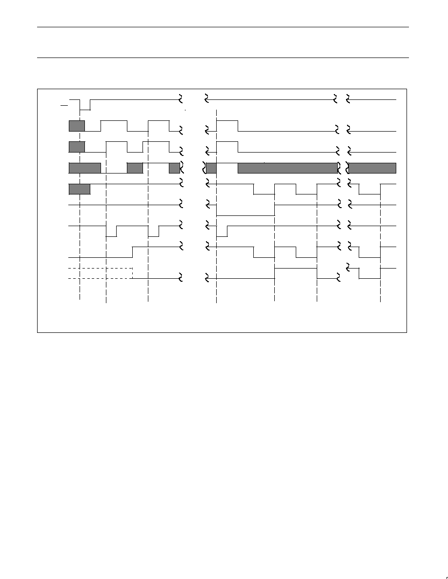
TYPICAL TIMING DIAGRAM
Clear
Load
word 1
Word 1
Word 2
Word 1
Load
word 2
Unload
word 2
Word
16
Unload
word 3
Load
words
3≠15
Word 3
is Low
Load
word 16
Unload
words
4≠15
Word 1
Word 2
Word 3
Unload
word 16
Word 16
MR
CPA
CPB
Dn
UNCPIN
IR
UNCPOUT
OR
Qn
SF00338
NOTE: Shaded areas Indicates irrelevant input conditions.
Philips Semiconductors
Product specification
74F225
16
◊
5 asynchronous FIFO (3-State)
June 15, 1992
9
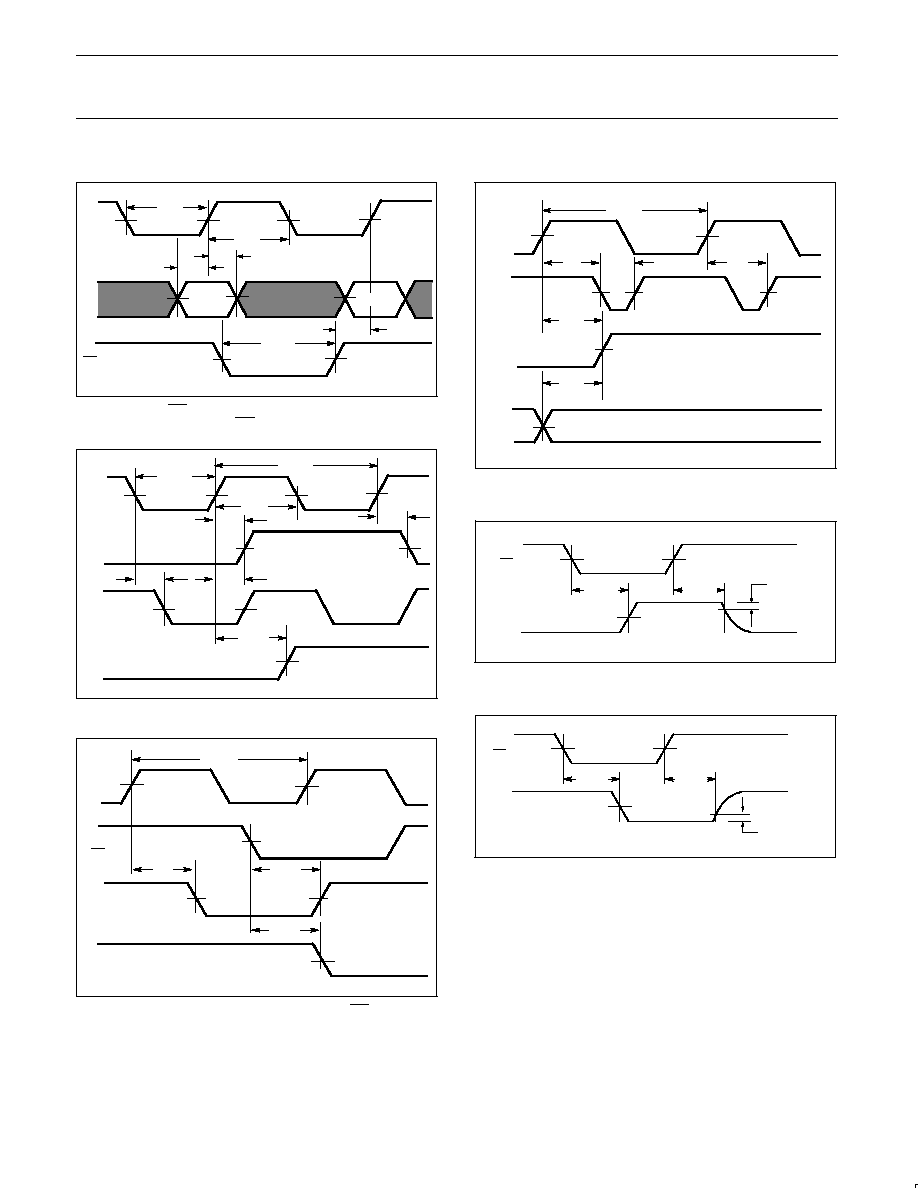
AC WAVEFORMS
VM
VM
MR
VM
VM
VM
CP
tsu
th
VM
tw(L)
VM
VM
VM
Dn
tsu
tw(H)
tw(L)
SF00339
Waveform 1. MR and Clock Pulse Widths, Data Setup and
Hold Times and MR to Clock Setup Time
VM
IR
VM
VM
UNCPIN
VM
tPLH
VM
VM
tPHL
VM
VM
OR
1/fMAX
tPLH
tPHL
Qn
tPLH
tw(L)
VM
tw(H)
SF00340
Waveform 2. UNCPIN to Output Delays
VM
OR
VM
CPA
or
CPB
VM
VM
IR
1/f
MAX
tPLH
tPHL
MR
VM
VM
tPHL
SF00341
Waveform 3. CPA or CPB to IR Delay and MR to IR
and OR Delay
VM
Qn
VM
VM
VM
OR
1/f
MAX
tPLH
tPHL
UNCPOUT
VM
tSK
tw(L)
VM
CPA
or
CPB
VM
tPLH
SF00342
Waveform 4. CPA or CPB to UNCPOUT and OR Delay,
UNCPOUT Pulse Width and Qn to OR Skew
VM
VM
VM
tPHZ
tPZH
VOH -0.3V
0V
OE
Qn
SF00343
Waveform 5. 3-State Output Enable Time to High Level and
Output Disable Time from High Level
VM
VM
VM
tPLZ
tPZL
VOL +0.3V
Qn
OE
SF00344
Waveform 6. 3-State Output Enable Time to Low Level and
Output Disable Time from Low Level
NOTES:
1. For all waveforms, V
M
= 1.5V.
2. The shaded areas indicate when the input is permitted to change for predictable output performance.
Philips Semiconductors
Product specification
74F225
16
◊
5 asynchronous FIFO (3-State)
June 15, 1992
10
APPLICATION
OR
UNCPIN
Q0
Q1
Q2
Q3
Q4
CPA
CPB
UNCPOUT
IR
D0
D1
D2
D3
D4
NC
CPA
CPB
UNCPOUT
IR
D0
D1
D2
D3
D4
MR
OE
OR
UNCPIN
Q0
Q1
Q2
Q3
Q4
MR
OE
MR
OE
MR
OE
NC
NC
NC
MR
OE
MR
OE
Output enable
NC
NC
Output ready
Unload clock
5≠bit data output
5≠bit data output
Load clock
5≠bit data input
Master reset
Input ready
5≠bit data input
CPA
CPB
UNCPOUT
IR
D0
D1
D2
D3
D4
OR
UNCPIN
Q0
Q1
Q2
Q3
Q4
CPA
CPB
UNCPOUT
IR
D0
D1
D2
D3
D4
OR
UNCPIN
Q0
Q1
Q2
Q3
Q4
CPA
CPB
UNCPOUT
IR
D0
D1
D2
D3
D4
OR
UNCPIN
Q0
Q1
Q2
Q3
Q4
CPA
CPB
UNCPOUT
IR
D0
D1
D2
D3
D4
OR
UNCPIN
Q0
Q1
Q2
Q3
Q4
SF00345
Figure 1. Expanding the 74F225 FIFO (48 words of 10 bits)
TEST CIRCUIT AND WAVEFORM
tw
90%
VM
10%
90%
VM
10%
90%
VM
10%
90%
VM
10%
NEGATIVE
PULSE
POSITIVE
PULSE
tw
AMP (V)
0V
0V
tTHL (tf
)
INPUT PULSE REQUIREMENTS
rep. rate
t
w
t
TLH
t
THL
1MHz
500ns
2.5ns
2.5ns
Input Pulse Definition
VCC
family
74F
D.U.T.
PULSE
GENERATOR
RL
CL
RT
VIN
VOUT
Test Circuit for Open Collector Outputs
DEFINITIONS:
R
L
= Load resistor;
see AC electrical characteristics for value.
C
L
= Load capacitance includes jig and probe capacitance;
see AC electrical characteristics for value.
R
T
= Termination resistance should be equal to Z
OUT
of
pulse generators.
tTHL (tf
)
tTLH (tr
)
tTLH (tr
)
AMP (V)
amplitude
3.0V
1.5V
V
M
RL
7.0V
SF00128
TEST
SWITCH
t
PLZ
closed
t
PZL
closed
All other
open
SWITCH POSITION

Philips Semiconductors
Product specification
74F225
16X5 asynchronous FIFO (3-State)
1992 Jun 15
11
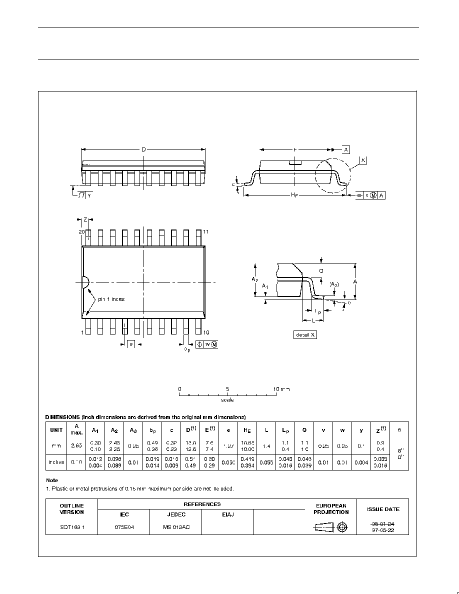
DIP20:
plastic dual in-line package; 20 leads (300 mil)
SOT146-1
Philips Semiconductors
Product specification
74F225
16X5 asynchronous FIFO (3-State)
1992 Jun 15
12
SO20:
plastic small outline package; 20 leads; body width 7.5 mm
SOT163-1

Philips Semiconductors
Product specification
74F225
16X5 asynchronous FIFO (3-State)
1992 Jun 15
13
NOTES
Philips Semiconductors
Product specification
74F225
16X5 asynchronous FIFO (3-State)
yyyy mmm dd
14
Definitions
Short-form specification -- The data in a short-form specification is extracted from a full data sheet with the same type number and title. For
detailed information see the relevant data sheet or data handbook.
Limiting values definition -- Limiting values given are in accordance with the Absolute Maximum Rating System (IEC 134). Stress above one
or more of the limiting values may cause permanent damage to the device. These are stress ratings only and operation of the device at these or
at any other conditions above those given in the Characteristics sections of the specification is not implied. Exposure to limiting values for extended
periods may affect device reliability.
Application information -- Applications that are described herein for any of these products are for illustrative purposes only. Philips
Semiconductors make no representation or warranty that such applications will be suitable for the specified use without further testing or
modification.
Disclaimers
Life support -- These products are not designed for use in life support appliances, devices or systems where malfunction of these products can
reasonably be expected to result in personal injury. Philips Semiconductors customers using or selling these products for use in such applications
do so at their own risk and agree to fully indemnify Philips Semiconductors for any damages resulting from such application.
Right to make changes -- Philips Semiconductors reserves the right to make changes, without notice, in the products, including circuits, standard
cells, and/or software, described or contained herein in order to improve design and/or performance. Philips Semiconductors assumes no
responsibility or liability for the use of any of these products, conveys no license or title under any patent, copyright, or mask work right to these
products, and makes no representations or warranties that these products are free from patent, copyright, or mask work right infringement, unless
otherwise specified.
Philips Semiconductors
811 East Arques Avenue
P.O. Box 3409
Sunnyvale, California 94088≠3409
Telephone 800-234-7381
©
Copyright Philips Electronics North America Corporation 1998
All rights reserved. Printed in U.S.A.
print code
Date of release: 10-98
Document order number:
9397-750-05099
Philips
Semiconductors
Data sheet
status
Objective
specification
Preliminary
specification
Product
specification
Product
status
Development
Qualification
Production
Definition
[1]
This data sheet contains the design target or goal specifications for product development.
Specification may change in any manner without notice.
This data sheet contains preliminary data, and supplementary data will be published at a later date.
Philips Semiconductors reserves the right to make chages at any time without notice in order to
improve design and supply the best possible product.
This data sheet contains final specifications. Philips Semiconductors reserves the right to make
changes at any time without notice in order to improve design and supply the best possible product.
Data sheet status
[1]
Please consult the most recently issued datasheet before initiating or completing a design.