 | –≠–ª–µ–∫—Ç—Ä–æ–Ω–Ω—ã–π –∫–æ–º–ø–æ–Ω–µ–Ω—Ç: N74F245N | –°–∫–∞—á–∞—Ç—å:  PDF PDF  ZIP ZIP |
Philips Semiconductors
74F245
Octal transceiver (3-State)
Product specification
1994 Nov 15
INTEGRATED CIRCUITS
IC15 Data Handbook
Philips Semiconductors
Product specification
74F245
Octal transceiver (3-State)
2
November 15, 1994
853≠0025 14256
FEATURES
∑
Octal bidirectional bus interface
∑
3-State buffer outputs sink 64mA
∑
15mA source current
∑
Outputs are placed in high impedance state during power-off
conditions
DESCRIPTION
The 74F245 is an octal transceiver featuring non-inverting 3-State
bus compatible outputs in both transmit and receive directions. The
B port outputs are capable of sinking 64mA and sourcing 15mA,
producing very good capacitive drive characteristics. The device
features an Output Enable (OE) input for easy cascading and
Transmit/Receive (T/R) input for direction control. The 3-State
outputs, B0≠B7, have been designed to prevent output bus loading if
the power is removed from the device.
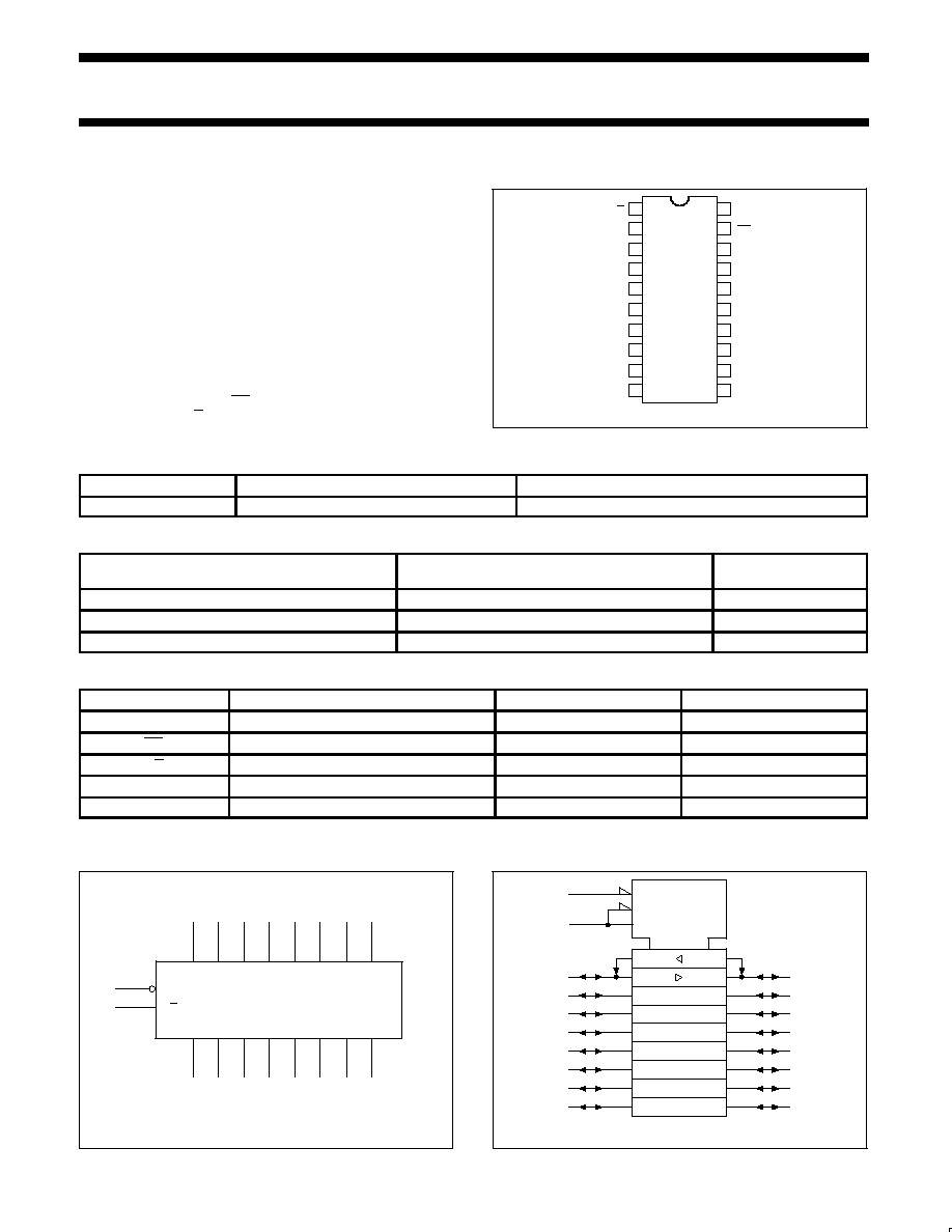
PIN CONFIGURATION
SF00198
1
2
3
4
5
6
7
8
9
10
11
12
13
14
15
16
17
18
19
20
T/R
A0
A1
A2
A3
A4
A5
A6
A7
GND
V
CC
OE
B0
B1
B2
B3
B4
B6
B5
B7
TYPE
TYPICAL PROPAGATION DELAY
TYPICAL SUPPLY CURRENT (TOTAL)
74F245
4.0ns
70mA
ORDERING INFORMATION
DESCRIPTION
COMMERCIAL RANGE
V
CC
= 5V
±
10%, T
amb
= 0
∞
C to +70
∞
C
DRAWING NUMBER
20-Pin Plastic DIP
N74F245N
SOT146-1
20-Pin Plastic SO
N74F245D
SOT163-1
20-Pin Plastic SSOP Type II
N74F245DB
SOT339-1
INPUT AND OUTPUT LOADING AND FAN-OUT TABLE
PINS
DESCRIPTION
74F (U.L.) HIGH/LOW
LOAD VALUE HIGH/LOW
A0≠A7, B0≠B7
Data inputs
3.5/1.0
70
µ
A/0.6mA
OE
Output Enable input (active Low)
1.0/2.0
20
µ
A/1.2mA
T/R
Transmit/Receive input
1.0/2.0
20
µ
A/1.2mA
A0≠A7
A port outputs
150/40
3.0mA/24mA
B0≠B7
B port outputs
750/106.7
15mA/64mA
NOTE: One (1.0) FAST unit load is defined as: 20
µ
A in the High state and 0.6mA in the Low state.
LOGIC SYMBOL
B2
B3
B4
B5
16
15
14
13
2
3
4
V
CC
= Pin 20
GND = Pin 10
SF00199
B1
17
B0
18
19
1
OE
T/R
A0
A1
A2
A3
A4
A5
5
6
7
B6
B7
12
11
A6
A7
8
9
IEC/IEEE SYMBOL
SF00200
G3
19
3EN1 (BA)
1
3EN1 (AB)
1
2
2
3
4
5
6
7
8
9
18
17
16
15
14
13
12
11
Philips Semiconductors
Product specification
74F245
Octal transceiver (3-State)
November 15, 1994
3
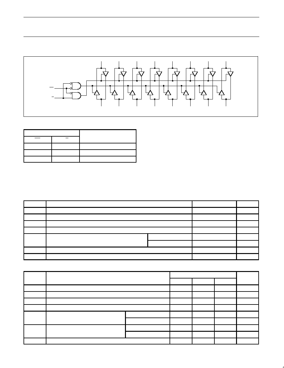
LOGIC DIAGRAM
SF00201
18
B0
17
B1
16
B2
15
B3
14
B4
13
B5
12
B6
11
B7
A0
A1
A2
A3
A4
A5
A6
A7
2
3
4
5
6
7
8
9
19
1
OE
T/R
V
CC
= Pin 20
GND = Pin 10
FUNCTION TABLE
INPUTS
OUTPUTS
OE
T/R
OUTPUTS
L
L
Bus B data to Bus A
L
H
Bus A data to Bus B
H
X
Z
H = High voltage level
L = Low voltage level
X = Don't care
Z = High impedance "off" state
ABSOLUTE MAXIMUM RATINGS
(Operation beyond the limits set forth in this table may impair the useful life of the device.
Unless otherwise noted these limits are over the operating free-air temperature range.)
SYMBOL
PARAMETER
RATING
UNIT
V
CC
Supply voltage
≠0.5 to +7.0
V
V
IN
Input voltage
≠0.5 to +7.0
V
I
IN
Input current
≠30 to +5
mA
V
OUT
Voltage applied to output in High output state
≠0.5 to +5.5
V
I
Current applied to output in Low output state
A0≠A7
48
mA
I
OUT
Current applied to output in Low output state
B0≠B7
128
mA
T
amb
Operating free-air temperature range
0 to +70
∞
C
T
stg
Storage temperature range
≠65 to +150
∞
C
RECOMMENDED OPERATING CONDITIONS
SYMBOL
PARAMETER
LIMITS
UNIT
SYMBOL
PARAMETER
MIN
NOM
MAX
UNIT
V
CC
Supply voltage
4.5
5.0
5.5
V
V
IH
High-level input voltage
2.0
V
V
IL
Low-level input voltage
0.8
V
I
IK
Input clamp current
≠18
mA
I
O
High level output current
A0≠A7
≠3
mA
I
OH
High-level output current
B0≠B7
≠15
mA
I
O
Low level output current
A0≠A7
24
mA
I
OL
Low-level output current
B0≠B7
64
mA
T
amb
Operating free-air temperature range
0
+70
∞
C
Philips Semiconductors
Product specification
74F245
Octal transceiver (3-State)
November 15, 1994
4
DC ELECTRICAL CHARACTERISTICS
(Over recommended operating free-air temperature range unless otherwise noted.)
SYMBOL
PARAMETER
TEST CONDITIONS
1
LIMITS
UNIT
SYMBOL
PARAMETER
TEST CONDITIONS
1
MIN
TYP
2
MAX
UNIT
A0 A7 B0 B7
I
O
= 3mA
±
10% V
CC
2.4
V
V
O
High level output voltage
A0≠A7, B0≠B7
V
CC
= MIN,
V
IL
= MAX
I
OH
= ≠3mA
±
5% V
CC
2.7
3.4
V
V
OH
High-level output voltage
B0 B7
V
IL
= MAX,
V
IH
= MIN
I
O
= 15mA
±
10% V
CC
2.0
V
B0≠B7
I
OH
= ≠15mA
±
5% V
CC
2.0
V
A0 A7
V
CC
= MIN
I
OL
= 20mA
±
10% V
CC
0.30
0.50
V
V
OL
Low-level output voltage
A0≠A7
V
CC
= MIN,
V
IL
= MAX,
V
MIN
I
OL
= 24mA
±
5% V
CC
0.35
0.50
V
B0≠B7
V
IH
= MIN
I
OL
= MAX
±
10% V
CC
0.55
V
V
OL
Low-level output voltage
B0≠B7
V
CC
= MIN,
V
IL
= MAX,
V
IH
= MIN
I
OL
= MAX
±
5% V
CC
0.42
0.55
V
V
IK
Input clamp voltage
V
CC
= MIN, I
I
= I
IK
≠0.73
≠1.2
V
I
Input current at maximum
OE, T/R
V
CC
= 5.5V, V
I
= 7.0V
100
µ
A
I
I
input voltage
A0≠A7, B0≠B7
V
CC
= 5.5V, V
I
= 5.5V
1
mA
I
IH
High-level input current
OE, T/R only
V
CC
= MAX, V
I
= 2.7V
20
µ
A
I
IL
Low-level input current
OE, T/R only
V
CC
= MAX, V
I
= 0.5V
≠1.2
mA
I
IH
+I
OZH
Off-state output current
High level voltage applied
V
CC
= MAX, V
O
= 2.7V
70
µ
A
I
IL
+I
OZL
Off-state output current
Low level voltage applied
V
CC
= MAX, V
O
= 0.5V
≠600
µ
A
I
OS
Short circuit output current
3
A0≠A7
V
CC
= MAX
≠60
≠150
mA
I
OS
Short-circuit output current
3
B0≠B7
V
CC
= MAX
≠100
≠225
mA
I
CCH
60
87
mA
I
CC
Supply current (total)
I
CCL
V
CC
= MAX
70
100
mA
I
CCZ
75
110
mA
NOTES:
1. For conditions shown as MIN or MAX, use the appropriate value specified under recommended operating conditions for the applicable type.
2. All typical values are at V
CC
= 5V, T
amb
= 25
∞
C.
3. Not more than one output should be shorted at a time. For testing I
OS
, the use of high-speed test apparatus and/or sample-and-hold
techniques are preferable in order to minimize internal heating and more accurately reflect operational values. Otherwise, prolonged shorting
of a High output may raise the chip temperature well above normal and thereby cause invalid readings in other parameter tests. In any
sequence of parameter tests, I
OS
tests should be performed last.
AC ELECTRICAL CHARACTERISTICS
LIMITS
SYMBOL
PARAMETER
TEST
CONDITION
V
CC
= +5.0V
T
amb
= +25
∞
C
C
L
= 50pF, R
L
= 500
V
CC
= +5.0V
±
10%
T
amb
= 0
∞
C to +70
∞
C
C
L
= 50pF, R
L
= 500
UNIT
MIN
TYP
MAX
MIN
MAX
t
PLH
t
PHL
Propagation delay
An to Bn, Bn to An
Waveform 1
2.5
2.5
3.5
4.0
6.0
6.0
2.5
2.5
7.0
7.0
ns
t
PZH
t
PZL
Output Enable time
to High or Low level
Waveform 2
Waveform 3
2.0
3.5
4.5
5.5
7.0
8.0
2.0
3.5
8.0
9.0
ns
t
PHZ
t
PLZ
Output Disable time
from High or Low level
Waveform 2
Waveform 3
2.5
1.0
5.0
3.5
6.5
6.0
2.0
1.0
7.5
7.0
ns
Philips Semiconductors
Product specification
74F245
Octal transceiver (3-State)
November 15, 1994
5
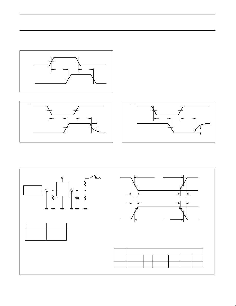
AC WAVEFORMS
For all waveforms, V
M
= 1.5V.
V
M
V
M
V
M
V
M
Bn, An
An, Bn
t
PLH
t
PHL
SF00202
Waveform 1.
Propagation Delay for Non-Inverting Output
VOH≠0.3V
VM
VM
VM
An, Bn
tPZH
tPHZ
SF00203
OE
0V
Waveform 2.
3-State Output Enable Time to High Level and
Output Disable Time from High Level
VOL+0.3V
VM
VM
VM
An, Bn
tPZL
tPLZ
SF00204
OE
Waveform 3.
3-State Output Enable Time to Low Level and
Output Disable Time from Low Level
TEST CIRCUIT AND WAVEFORMS
tw
90%
VM
10%
90%
VM
10%
90%
VM
10%
90%
VM
10%
NEGATIVE
PULSE
POSITIVE
PULSE
tw
AMP (V)
0V
0V
tTHL (tf
)
INPUT PULSE REQUIREMENTS
rep. rate
t
w
t
TLH
t
THL
1MHz
500ns
2.5ns
2.5ns
Input Pulse Definition
VCC
family
74F
D.U.T.
PULSE
GENERATOR
RL
CL
RT
VIN
VOUT
Test Circuit for Open Collector Outputs
DEFINITIONS:
R
L
= Load resistor;
see AC electrical characteristics for value.
C
L
= Load capacitance includes jig and probe capacitance;
see AC electrical characteristics for value.
R
T
= Termination resistance should be equal to Z
OUT
of
pulse generators.
tTHL (tf
)
tTLH (tr
)
tTLH (tr
)
AMP (V)
amplitude
3.0V
1.5V
V
M
RL
7.0V
SF00128
TEST
SWITCH
t
PLZ
closed
t
PZL
closed
All other
open
SWITCH POSITION
Philips Semiconductors
Product specification
74F245
Octal transceiver (3-State)
1994 Nov 15
6
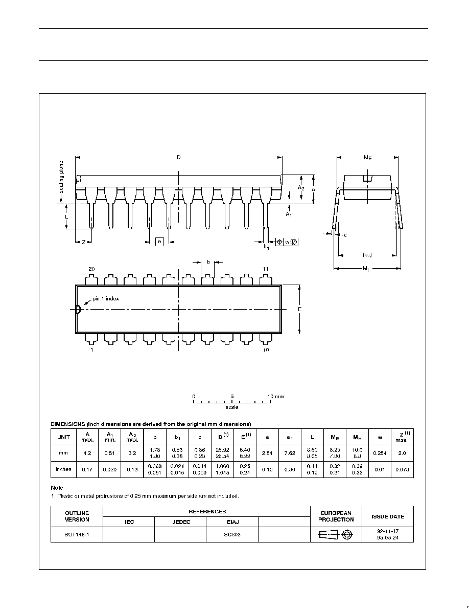
DIP20:
plastic dual in-line package; 20 leads (300 mil)
SOT146-1
Philips Semiconductors
Product specification
74F245
Octal transceiver (3-State)
1994 Nov 15
7
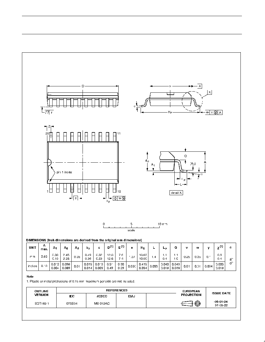
SO20:
plastic small outline package; 20 leads; body width 7.5 mm
SOT163-1

Philips Semiconductors
Product specification
74F245
Octal transceiver (3-State)
1994 Nov 15
8
NOTES
Philips Semiconductors
Product specification
74F245
Octal transceiver (3-State)
1994 Nov 15
9
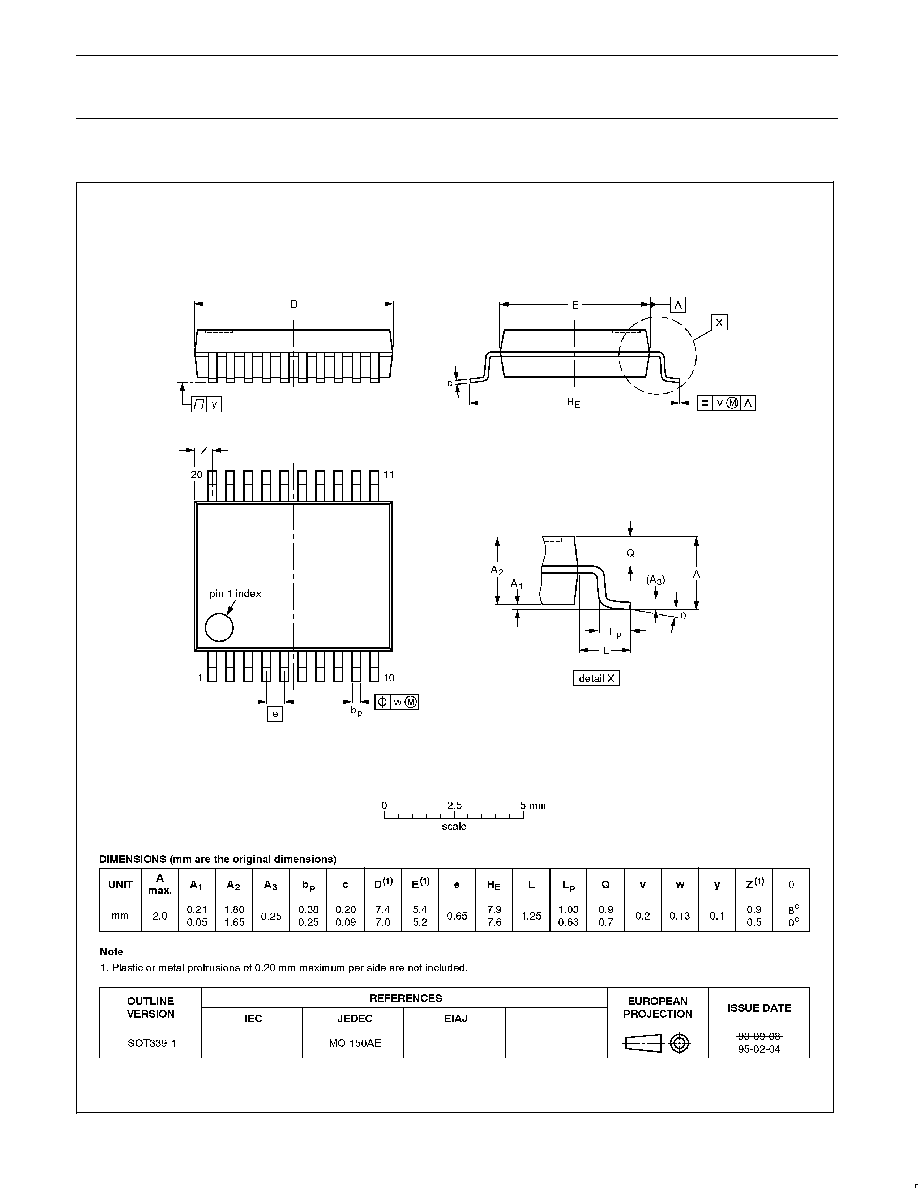
SSOP20:
plastic shrink small outline package; 20 leads; body width 5.3 mm
SOT339-1

Philips Semiconductors
Product specification
74F245
Octal transceiver (3-State)
Philips Semiconductors and Philips Electronics North America Corporation reserve the right to make changes, without notice, in the products,
including circuits, standard cells, and/or software, described or contained herein in order to improve design and/or performance. Philips
Semiconductors assumes no responsibility or liability for the use of any of these products, conveys no license or title under any patent, copyright,
or mask work right to these products, and makes no representations or warranties that these products are free from patent, copyright, or mask
work right infringement, unless otherwise specified. Applications that are described herein for any of these products are for illustrative purposes
only. Philips Semiconductors makes no representation or warranty that such applications will be suitable for the specified use without further testing
or modification.
LIFE SUPPORT APPLICATIONS
Philips Semiconductors and Philips Electronics North America Corporation Products are not designed for use in life support appliances, devices,
or systems where malfunction of a Philips Semiconductors and Philips Electronics North America Corporation Product can reasonably be expected
to result in a personal injury. Philips Semiconductors and Philips Electronics North America Corporation customers using or selling Philips
Semiconductors and Philips Electronics North America Corporation Products for use in such applications do so at their own risk and agree to fully
indemnify Philips Semiconductors and Philips Electronics North America Corporation for any damages resulting from such improper use or sale.
This data sheet contains preliminary data, and supplementary data will be published at a later date. Philips
Semiconductors reserves the right to make changes at any time without notice in order to improve design
and supply the best possible product.
Philips Semiconductors
811 East Arques Avenue
P.O. Box 3409
Sunnyvale, California 94088≠3409
Telephone 800-234-7381
DEFINITIONS
Data Sheet Identification
Product Status
Definition
Objective Specification
Preliminary Specification
Product Specification
Formative or in Design
Preproduction Product
Full Production
This data sheet contains the design target or goal specifications for product development. Specifications
may change in any manner without notice.
This data sheet contains Final Specifications. Philips Semiconductors reserves the right to make changes
at any time without notice, in order to improve design and supply the best possible product.
Philips Semiconductors and Philips Electronics North America Corporation
register eligible circuits under the Semiconductor Chip Protection Act.
©
Copyright Philips Electronics North America Corporation 1996
All rights reserved. Printed in U.S.A.
(print code)
Date of release: July 1994
Document order number:
9397-750-05104