 | –≠–ª–µ–∫—Ç—Ä–æ–Ω–Ω—ã–π –∫–æ–º–ø–æ–Ω–µ–Ω—Ç: N74F251AN | –°–∫–∞—á–∞—Ç—å:  PDF PDF  ZIP ZIP |
Document Outline
- FEATURES
- DESCRIPTION
- PIN CONFIGURATION
- ORDERING INFORMATION
- INPUT AND OUTPUT LOADING AND FAN-OUT TABLE
- LOGIC SYMBOL
- IEC/IEEE SYMBOL
- LOGIC DIAGRAM
- FUNCTION TABLE
- ABSOLUTE MAXIMUM RATINGS
- RECOMMENDED OPERATING CONDITIONS
- DC ELECTRICAL CHARACTERISTICS
- AC ELECTRICAL CHARACTERISTICS
- AC WAVEFORMS
- TEST CIRCUIT AND WAVEFORMS
Philips Semiconductors
Product specification
74F251A
8-input multiplexer (3-State)
1
1996 Jan 05
853≠0358 16191
FEATURES
∑
High speed 8-to-1 multiplexing
∑
On chip decoding
∑
Multifunction capability
∑
Inverting and Non-Inverting outputs
∑
Both outputs are 3-State for further multiplexer expansion
DESCRIPTION
The 74F251A is a logic implementation of a single 8-position switch
with the switch position controlled by the state of three Select (S0,
S1, S2) inputs. True (Y) and complementary (Y) outputs are both
provided. The output enable (OE) is active Low. When OE is High,
both outputs are in High impedance state, allowing multiple output
connections to a common bus without driving nor loading the bus
significantly. All but one device must be in High impedance state to
avoid high currents that would exceed the maximum ratings when
the outputs of the 3-State devices are tied together. When the output
of more than one device is tied together the user must ensure that
there is no overlap in the active Low portion of the output enable
voltages.
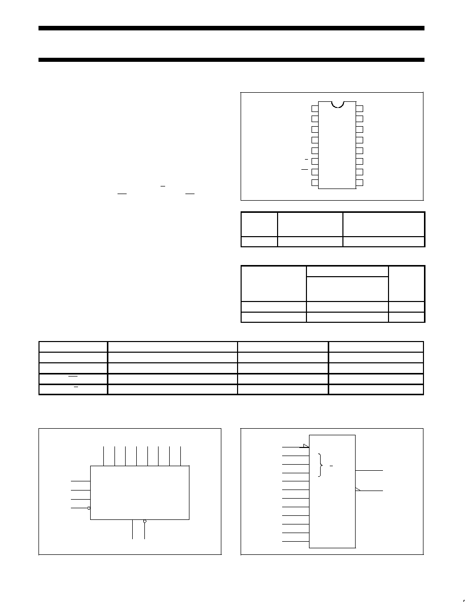
PIN CONFIGURATION
16
15
14
13
12
11
10
7
6
5
4
3
2
1
OE
V
CC
I7
S0
S1
I6
I4
I5
I3
I2
Y
I1
I0
Y
9
8
GND
S2
SF00778
TYPE
TYPICAL
PROPAGATION
DELAY
TYPICAL
SUPPLY CURRENT
(TOTAL)
74F251A
4.5ns
19mA
ORDERING INFORMATION
DESCRIPTION
ORDER CODE
PKG
DESCRIPTION
COMMERCIAL RANGE
V
CC
= 5V
±
10%,
T
amb
= 0
∞
C to +70
∞
C
PKG
DWG #
16-pin plastic DIP
N74F251AN
SOT38-4
16-pin plastic SO
N74F251AD
SOT162-1
INPUT AND OUTPUT LOADING AND FAN-OUT TABLE
PINS
DESCRIPTION
74F (U.L.) HIGH/LOW
LOAD VALUE HIGH/LOW
I0≠I7
Data inputs
1.0/1.0
20
µ
A/0.6mA
S0≠S2
Select inputs
1.0/1.0
20
µ
A/0.6mA
OE
Output Enable input (active Low)
1.0/1.0
20
µ
A/0.6mA
Y, Y
Data outputs
150/40
3mA/24mA
NOTE:
One (1.0) FAST unit load is defined as: 20
µ
A in the High state and 0.6mA in the Low state.
LOGIC SYMBOL
1
2
3
V
CC
= Pin 16
GND = Pin 8
SF00779
6
5
11
10
9
S0
S1
S2
7
4
12
13
14
15
OE
Y
Y
I0
I1
I2
I3
I4
I5
I6
I7
IEC/IEEE SYMBOL
SF00780
MUX
7
11
3
2
1
5
6
0
G
0
7
10
2
EN
9
4
14
13
12
15
Philips Semiconductors
Product specification
74F251A
8-input multiplexer (3-State)
1996 Jan 05
2
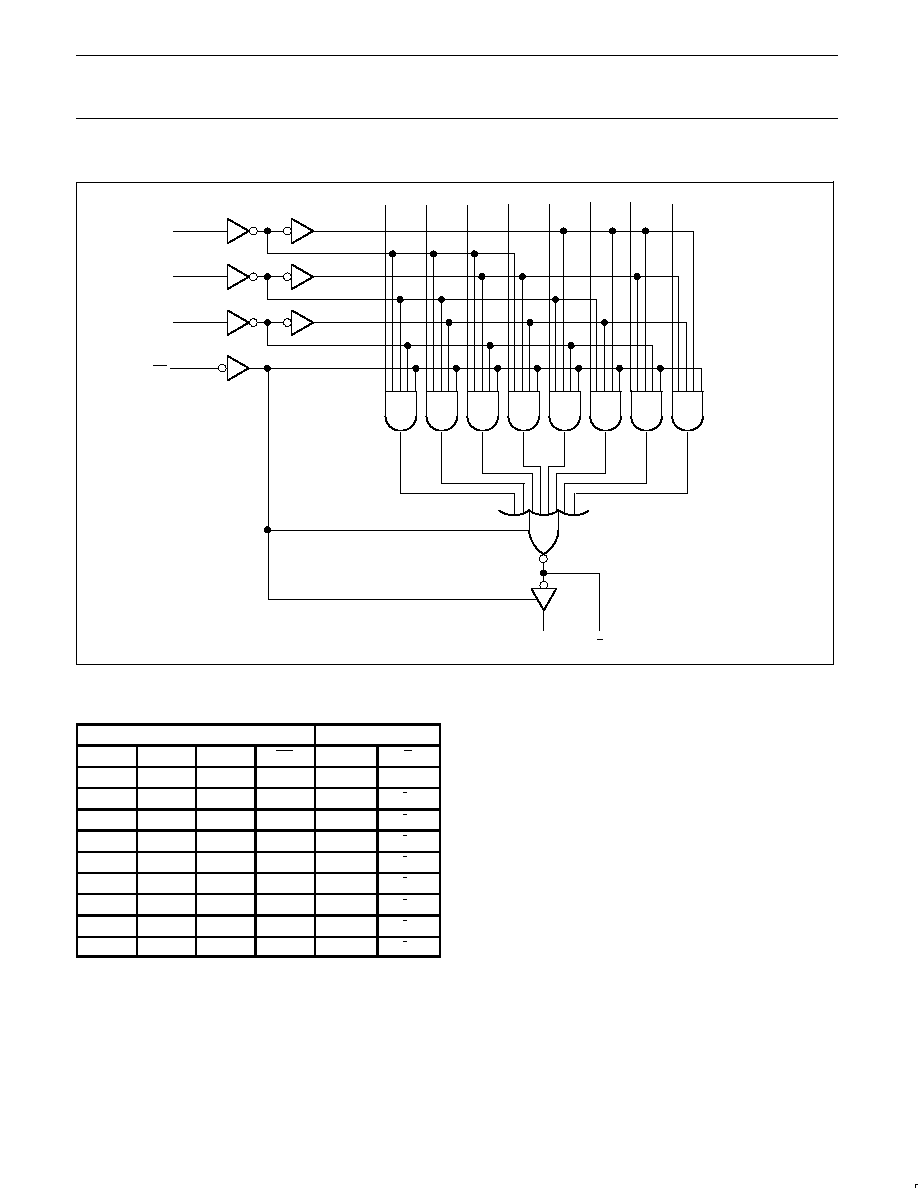
LOGIC DIAGRAM
9
10
11
V
CC
= Pin 16
GND = Pin 8
SF00781
Y
Y
5
6
4
3
2
1
15
14
13
12
I0
I1
I2
I3
I4
I5
I6
I7
7
OE
S0
S1
S2
FUNCTION TABLE
INPUTS
OUTPUTS
S2
S1
S0
OE
Y
Y
X
X
X
H
Z
Z
L
L
L
L
I0
I0
L
L
H
L
I1
I1
L
H
L
L
I2
I2
L
H
H
L
I3
I3
H
L
L
L
I4
I4
H
L
H
L
I5
I5
H
H
L
L
I6
I6
H
H
H
L
I7
I7
NOTES:
H = High voltage level
L
= Low voltage level
X = Don't care
Z = High impedance "off" state
Philips Semiconductors
Product specification
74F251A
8-input multiplexer (3-State)
1996 Jan 05
3
ABSOLUTE MAXIMUM RATINGS
(Operation beyond the limit set forth in this table may impair the useful life of the device.
Unless otherwise noted these limits are over the operating free air temperature range.)
SYMBOL
PARAMETER
RATING
UNIT
V
CC
Supply voltage
≠0.5 to +7.0
V
V
IN
Input voltage
≠0.5 to +7.0
V
I
IN
Input current
≠30 to +5
mA
V
OUT
Voltage applied to output in High output state
≠0.5 to V
CC
V
I
OUT
Current applied to output in Low output state
48
mA
T
amb
Operating free-air temperature range
0 to +70
∞
C
T
stg
Storage temperature
≠65 to +150
∞
C
RECOMMENDED OPERATING CONDITIONS
SYMBOL
PARAMETER
LIMITS
UNIT
SYMBOL
PARAMETER
MIN
NOM
MAX
UNIT
V
CC
Supply voltage
4.5
5.0
5.5
V
V
IH
High-level input voltage
2.0
V
V
IL
Low-level input voltage
0.8
V
I
IK
Input clamp current
≠18
mA
I
OH
High-level output current
≠3
mA
I
OL
Low-level output current
24
mA
T
amb
Operating free-air temperature range
0
70
∞
C
DC ELECTRICAL CHARACTERISTICS
(Over recommended operating free-air temperature range unless otherwise noted.)
SYMBOL
PARAMETER
TEST CONDITIONS
1
LIMITS
UNIT
SYMBOL
PARAMETER
TEST CONDITIONS
1
MIN
TYP
2
MAX
UNIT
V
OH
High-level output voltage
V
CC
= MIN, V
IL
= MAX,
±
10%V
CC
2.4
V
V
OH
High-level output voltage
V
CC
MIN, V
IL
MAX,
V
IH
= MIN, I
OH
= MAX
±
5%V
CC
2.7
3.3
V
V
OL
Low-level output voltage
V
CC
= MIN, V
IL
= MAX,
±
10%V
CC
0.35
0.50
V
V
OL
Low-level output voltage
V
CC
MIN, V
IL
MAX,
V
IH
= MIN, I
OL
= MAX
±
5%V
CC
0.35
0.50
V
V
IK
Input clamp voltage
V
CC
= MIN, I
I
= I
IK
≠0.73
≠1.2
V
I
I
Input current at maximum input
voltage
V
CC
= MAX, V
I
= 7.0V
100
µ
A
I
IH
High-level input current
V
CC
= MAX, V
I
= 2.7V
20
µ
A
I
IL
Low-level input current
V
CC
= MAX, V
I
= 0.5V
≠0.6
mA
I
OZH
Off-state output current
High-level voltage applied
V
CC
= MAX, V
I
= 2.7V
50
µ
A
I
OZL
Off-state output current
Low-level voltage applied
V
CC
= MAX, V
I
= 0.5V
≠50
mA
I
OS
Short-circuit output current
3
V
CC
= MAX
≠60
≠150
mA
I
S
l
(
l)
I
CCH
V
MAX
20
27
mA
I
CC
Supply current (total)
I
CCL
V
CC
= MAX
17
24
mA
CC
pp y
(
)
I
CCZ
CC
21
29
mA
NOTES:
1. For conditions shown as MIN or MAX, use the appropriate value specified under recommended operating conditions for the applicable type.
2. All typical values are at V
CC
= 5V, T
amb
= 25
∞
C.
3. Not more than one output should be shorted at a time. For testing I
OS
, the use of high-speed test apparatus and/or sample-and-hold
techniques are preferable in order to minimize internal heating and more accurately reflect operational values. Otherwise, prolonged shorting
of a High output may raise the chip temperature well above normal and thereby cause invalid readings in other parameter tests. In any
sequence of parameter tests, I
OS
tests should be performed last.
Philips Semiconductors
Product specification
74F251A
8-input multiplexer (3-State)
1996 Jan 05
4
AC ELECTRICAL CHARACTERISTICS
SYMBOL
PARAMETER
TEST
LIMITS
UNIT
SYMBOL
PARAMETER
TEST
CONDITION
V
CC
= +5V
T
amb
= +25
∞
C
C
L
= 50pF
R
L
= 500
V
CC
= +5V
±
10%
T
amb
= 0
∞
C to +70
∞
C
C
L
= 50pF
R
L
= 500
UNIT
MIN
TYP
MAX
MIN
MAX
t
PLH
t
PHL
Propagation delay
In to Y
Waveform 2
3.0
3.0
5.0
5.0
7.0
7.0
2.5
3.0
8.0
8.0
ns
t
PLH
t
PHL
Propagation delay
In to Y
Waveform 1
2.5
1.0
4.5
2.5
7.0
5.0
2.0
1.0
7.5
5.0
ns
t
PLH
t
PHL
Propagation delay
Sn to Y
Waveform 1
Waveform 2
4.5
4.0
6.5
5.5
10.0
9.0
4.0
3.5
11.5
9.5
ns
t
PLH
t
PHL
Propagation delay
Sn to Y
Waveform 1
Waveform 2
3.5
2.5
6.0
4.5
9.0
7.0
3.5
2.5
9.5
7.5
ns
t
PZH
t
PZL
Output Enable time OE
to Y
Waveform 3
Waveform 4
3.5
3.5
5.5
5.0
7.5
7.5
3.0
3.0
8.5
8.0
ns
t
PHZ
t
PLZ
Output Disable time
OE to Y
Waveform 3
Waveform 4
2.5
1.0
4.0
4.0
6.5
6.0
2.0
1.0
7.0
6.5
ns
t
PZH
t
PZL
Output Enable time
OE to Y
Waveform 3
Waveform 4
2.5
2.5
4.0
4.0
6.5
6.5
2.0
2.5
7.0
7.0
ns
t
PHZ
t
PLZ
Output Disable time
OE to Y
Waveform 3
Waveform 4
3.5
1.0
5.0
2.0
7.5
4.5
3.0
1.0
8.0
4.5
ns
AC WAVEFORMS
For all waveforms, V
M
= 1.5V
V
M
V
M
V
M
V
M
V
OUT
V
IN
t
PHL
t
PLH
SF00782
Waveform 1.
For Inverting Outputs
V
M
V
M
V
M
V
M
V
OUT
V
IN
t
PLH
t
PHL
SF00092
Waveform 2. For Non-Inverting Outputs
V
M
V
M
V
M
t
PHZ
t
PZH
V
OH
≠0.3V
OE
SF00784
0V
Y, Y
Waveform 3.
3-State Output Enable Time to High Level and
Output Disable Time from High Level
V
M
V
M
V
M
t
PLZ
t
PZL
V
OL
+0.3V
OE
Y, Y
SF00785
Waveform 4.
3-State Output Enable Time to Low Level and
Output Disable Time from Low Level
Philips Semiconductors
Product specification
74F251A
8-input multiplexer (3-State)
1996 Jan 05
5
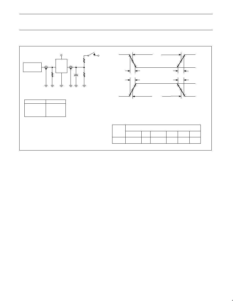
TEST CIRCUIT AND WAVEFORMS
tw
90%
VM
10%
90%
VM
10%
90%
VM
10%
90%
VM
10%
NEGATIVE
PULSE
POSITIVE
PULSE
tw
AMP (V)
0V
0V
tTHL (tf
)
INPUT PULSE REQUIREMENTS
rep. rate
t
w
t
TLH
t
THL
1MHz
500ns
2.5ns
2.5ns
Input Pulse Definition
VCC
family
74F
D.U.T.
PULSE
GENERATOR
RL
CL
RT
VIN
VOUT
Test Circuit for 3-State Outputs
DEFINITIONS:
R
L
= Load resistor;
see AC electrical characteristics for value.
C
L
= Load capacitance includes jig and probe capacitance;
see AC electrical characteristics for value.
R
T
= Termination resistance should be equal to Z
OUT
of
pulse generators.
tTHL (tf
)
tTLH (tr
)
tTLH (tr
)
AMP (V)
amplitude
3.0V
1.5V
V
M
RL
7.0V
SF00777
TEST
SWITCH
t
PLZ
closed
t
PZL
closed
All other
open
SWITCH POSITION