 | –≠–ª–µ–∫—Ç—Ä–æ–Ω–Ω—ã–π –∫–æ–º–ø–æ–Ω–µ–Ω—Ç: N74F257AD | –°–∫–∞—á–∞—Ç—å:  PDF PDF  ZIP ZIP |
Philips Semiconductors
74F257A
Quad 2-line to 1-line selector/multiplexer,
non-inverting (3-State)
Product specification
1995 Mar 31
INTEGRATED CIRCUITS
IC15 Data Handbook
Philips Semiconductors
Product specification
74F257A
Quad 2-line to 1-line selector/multiplexer, non-inverting
(3-State)
2
1995 Mar 31
853≠0360 15059
FEATURES
∑
Industrial range available (≠40
∞
C to +85
∞
C)
∑
Multifunction capability
∑
Non-inverting data path
∑
3-State outputs
∑
See 74F258A for inverting version
DESCRIPTION
The 74F257A has four identical 2-input multiplexers with 3-State
outputs which select 4 bits of data from two sources uncer control of
a common Select (S) input. The I0a inputs are selected when the
common Select input is Low and the I1n inputs are selected when
the common Select input is High. Data appears at the outputs in true
non-inverted form from the selected inputs. The 74F257A is the logic
implementation of a 4-pole, 2-position switch where the position of
the switch is determined by the logic levels supplied to the common
Slect input. Outputs are forced to a high impedance "off" state when
the Output Enable (OE) is High. All but one device must be in high
impedance state to avoid currents that would exceed the maximum
rating if the outputs were tied together. Design of the Output Enable
signals must ensure that there is no overlap when outputs of 3-state
devices were tied together.
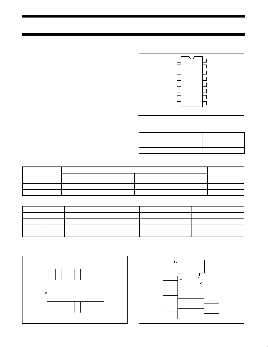
PIN CONFIGURATION
16
15
14
13
12
11
10
7
6
5
4
3
2
1
Yb
V
CC
Yd
I0c
I1c
I1d
OE
I0d
S
I0a
I1b
I1a
Ya
I0b
9
8
GND
Yc
SF00673
TYPE
TYPICAL
PROPAGATION DELAY
TYPICAL
SUPPLY CURRENT
(TOTAL)
74F257A
4.3ns
12mA
ORDERING INFORMATION
ORDER CODE
DRAWING
DESCRIPTION
COMMERCIAL RANGE
V
CC
= 5V
±
10%, T
amb
= 0
∞
C to +70
∞
C
INDUSTRIAL RANGE
V
CC
= 5V
±
10%, T
amb
= ≠40
∞
C to +85
∞
C
DRAWING
NUMBER
16-pin plastic DIP
N74F257AN
I74F257AN
SOT38-4
16-pin plastic SO
N74F257AD
I74F257AD
SOT109-1
INPUT AND OUTPUT LOADING AND FAN-OUT TABLE
PINS
DESCRIPTION
74F (U.L.) HIGH/LOW
LOAD VALUE HIGH/LOW
I0n, I1n
Data inputs
1.0/1.0
20
µ
A/0.6mA
S
Common Select input
1.0/1.0
20
µ
A/0.6mA
OE
Output Enable input (active Low)
1.0/1.0
20
µ
A/0.6mA
Ya ≠ Yd
Data outputs
150/33
3.0mA/20mA
NOTE:
One (1.0) FAST unit load is defined as: 20
µ
A in the High state and 0.6mA in the Low state.
LOGIC SYMBOL
V
CC
= Pin 16
GND = Pin 8
SF00674
1
15
S
OE
2
3
5
6
11
10
14
I0a
I1a
I0b
I1b
I0c
I1c
I0d
Ya
Yb
Yc
Yd
4
7
9
12
13
I1d
LOGIC SYMBOL (IEEE/IEC)
SF00675
2
1
15
EN
1
G1
3
4
1
MUX
5
6
7
10
11
9
13
14
12

Philips Semiconductors
Product specification
74F257A
Quad 2-line to 1-line selector/multiplexer, non-inverting
(3-State)
1995 Mar 31
3
LOGIC DIAGRAM
I0a
I1a
I0b
I1b
I0c
I1c
I0d
I1d
OE
S
2
3
5
6
11
10
14
13
15
1
4
7
9
12
Ya
Yb
Yc
Yd
V
CC
= Pin 16
GND = Pin 8
SF00676
FUNCTION TABLE
INPUTS
OUTPUT
OE
S
I0
I1
Y
H
X
X
X
Z
L
H
X
L
L
L
H
X
H
H
L
L
L
X
L
L
L
H
X
H
H
=
High voltage level
L
=
Low voltage level
X
=
Don't care
Z
=
High impedance "off" state
APPLICATION
SF00677
I0a I1a I0b I1b I0c I1c I0d I1d
Ya
Yb
Yc
Yd
I0a I1a I0b I1b I0c I1c I0d I1d
Ya
Yb
Yc
Yd
I0a I1a I0b I1b I0c I1c I0d I1d
Ya
Yb
Yc
Yd
I0a I1a I0b I1b I0c I1c I0d I1d
Ya
Yb
Yc
Yd
74F257A
74F257A
74F257A
74F257A
4-BIT
DATA
BUS
OE
S
OE
S
OE
S
OE
S
WORD A
WORD B
WORD C
WORD D
WORD E
WORD F
WORD G
WORD H
Y0
Y1
Y2
Y3
74F139
C
B
A
S2
S1
S0
ENABLE
Philips Semiconductors
Product specification
74F257A
Quad 2-line to 1-line selector/multiplexer, non-inverting
(3-State)
1995 Mar 31
4
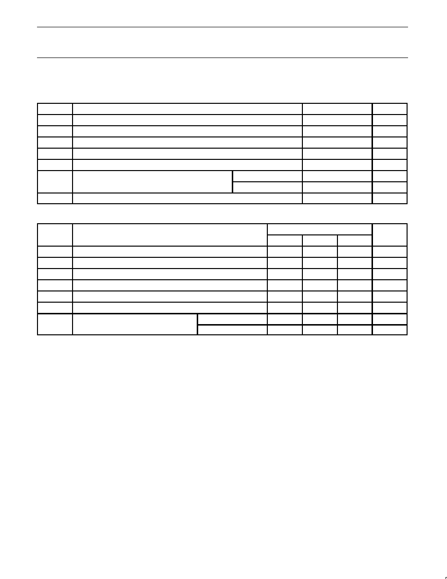
ABSOLUTE MAXIMUM RATINGS
(Operation beyond the limits set forth in this table may impair the useful life of the device.
Unless otherwise noted these limits are over the operating free-air temperature range.)
SYMBOL
PARAMETER
RATING
UNIT
V
CC
Supply voltage
≠0.5 to +7.0
V
V
IN
Input voltage
≠0.5 to +7.0
V
I
IN
Input current
≠30 to +5
mA
V
OUT
Voltage applied to output in High output state
≠0.5 to V
CC
V
I
OUT
Current applied to output in Low output state
48
mA
T
Operating free air temperature range
Commercial range
0 to +70
∞
C
T
amb
Operating free-air temperature range
Industrial range
≠40 to +85
∞
C
T
stg
Storage temperature range
≠65 to +150
∞
C
RECOMMENDED OPERATING CONDITIONS
SYMBOL
PARAMETER
LIMITS
UNIT
SYMBOL
PARAMETER
MIN
NOM
MAX
UNIT
V
CC
Supply voltage
4.5
5.0
5.5
V
V
IH
High-level input voltage
2.0
V
V
IL
Low-level input voltage
0.8
V
I
IK
Input clamp current
≠18
mA
I
OH
High-level output current
≠3
mA
I
OL
Low-level output current
24
mA
T
Operating free air temperature range
Commercial range
0
+70
∞
C
T
amb
Operating free-air temperature range
Industrial range
≠40
+85
∞
C

Philips Semiconductors
Product specification
74F257A
Quad 2-line to 1-line selector/multiplexer, non-inverting
(3-State)
1995 Mar 31
5
DC ELECTRICAL CHARACTERISTICS
(Over recommended operating free-air temperature range unless otherwise noted.)
SYMBOL
PARAMETER
TEST CONDITIONS
1
LIMITS
UNIT
SYMBOL
PARAMETER
TEST CONDITIONS
1
MIN
TYP
2
MAX
UNIT
V
O
High level output voltage
V
CC
= MIN, V
IL
= MAX,
±
10%V
CC
2.4
V
V
OH
High-level output voltage
CC
,
IL
,
V
IH
= MIN, I
OH
= MAX
±
5%V
CC
2.7
3.3
V
V
O
Low level output voltage
V
CC
= MIN, V
IL
= MAX,
±
10%V
CC
0.35
0.50
V
V
OL
Low-level output voltage
CC
,
IL
,
V
IH
= MIN, I
OL
= MAX
±
5%V
CC
0.35
0.50
V
V
IK
Input clamp voltage
V
CC
= MIN, I
I
= I
IK
≠0.73
≠1.2
V
I
I
Input current at maximum input voltage
V
CC
= MAX, V
I
= 7.0V
100
µ
A
I
IH
High-level input current
V
CC
= MAX, V
I
= 2.7V
20
µ
A
I
IL
Low-level input current
V
CC
= MAX, V
I
= 0.5V
≠0.6
mA
I
OZH
Off state output current,
High-level voltage applied
V
CC
= MAX, V
O
= 2.7V
50
µ
A
I
OZL
Off state output current,
Low-level voltage applied
V
CC
= MAX, V
O
= 0.5V
≠50
µ
A
I
OS
Short-circuit output current
3
V
CC
= MAX
-60
≠150
mA
4
I
CCH
9.0
15.0
mA
I
CC
Supply current
4
(total)
I
CCL
V
CC
= MAX
14.5
22.0
mA
I
CCZ
15.0
23.0
mA
NOTES:
1. For conditions shown as MIN or MAX, use the appropriate value specified under recommended operating conditions for the applicable type.
2. All typical values are at V
CC
= 5V, T
amb
= 25
∞
C.
3. Not more than one output should be shorted at a time. For testing I
OS
, the use of high-speed test apparatus and/or sample-and-hold
techniques are preferable in order to minimize internal heating and more accurately reflect operational values. Otherwise, prolonged shorting
of a High output may raise the chip temperature well above normal and thereby cause invalid readings in other parameter tests. In any
sequence of parameter tests, I
OS
tests should be performed last.
4. Measure I
CC
with all outputs open and inputs grounded.
AC ELECTRICAL CHARACTERISTICS
LIMITS
SYMBOL
PARAMETER
TEST
CONDITION
T
amb
= +25
∞
C
V
CC
= +5.0V
C
L
= 50pF
R
L
= 500
T
amb
= 0
∞
C to +70
∞
C
V
CC
= +5.0V
±
10%
C
L
= 50pF
R
L
= 500
T
amb
= ≠40
∞
C to +85
∞
C
V
CC
= +5.0V
±
10%
C
L
= 50pF
R
L
= 500
UNIT
MIN
TYP
MAX
MIN
MAX
MIN
MAX
t
PLH
t
PHL
Propagation delay
In to Yn
Waveform 1
3.0
2.0
4.5
3.5
6.0
5.0
3.0
2.0
7.0
6.0
3.0
2.0
7.0
7.0
ns
t
PLH
t
PHL
Propagation delay
S to Yn
Waveform 1
5.0
4.0
7.5
5.5
9.5
7.0
5.0
4.0
10.5
8.0
5.0
4.0
10.5
8.5
ns
t
PZH
t
PZL
Output Enable time
to High or Low level
Waveform 2
Waveform 3
4.5
4.5
6.5
6.0
7.5
7.5
4.5
4.5
8.5
8.5
4.5
4.5
8.5
8.5
ns
t
PHZ
t
PLZ
Output Disable time
from High or Low level
Waveform 2
Waveform 3
2.0
2.0
4.0
3.5
5.5
5.5
2.0
2.0
6.0
6.0
2.0
2.0
6.0
6.0
ns