 | –≠–ª–µ–∫—Ç—Ä–æ–Ω–Ω—ã–π –∫–æ–º–ø–æ–Ω–µ–Ω—Ç: N74F283D | –°–∫–∞—á–∞—Ç—å:  PDF PDF  ZIP ZIP |

Philips
Semiconductors
74F283
4-bit binary full adder with fast carry
Product specification
IC15 Data Handbook
1989 Mar 03
INTEGRATED CIRCUITS
Philips Semiconductors
Product specification
74F283
4-bit binary full adder with fast carry
2
1989 Mar 03
853-0364 95944
FEATURES
∑
High speed 4-bit addition
∑
Cascadable in 4-bit increments
∑
Fast Internal carry look-ahead
DESCRIPTION
The 74F283 adds two 4-bit binary words (An plus Bn) plus the
incoming carry. The binary sum appears on the sum outputs
(
0≠
3) and the outgoing carry (C
OUT
) according to the equation:
C
IN
+2
0
(A0+B0)+2
1
(A1+B1)+2
2
(A2+B2)+2
3
(A3+B3)
=
0+2
1+4
2+8
3+16C
OUT
where (+)=plus
Due to the symmetry of the binary add function, the 74F283 can be
used with either all active-High operands (positive logic) or with all
active-Low operands (negative logic). See Function Table. In case of
all active-Low operands (negative logic) the results
1≠
4 and C
OUT
should be interpreted also as active-Low. With active-High inputs,
C
IN
cannot be left open; it must be held Low when no "carry in" is
intended. Interchanging inputs of equal weight does not affect the
operation, thus A0, B0, C
IN
can arbitrarily be assigned to pins 5, 6,
7, etc.
Due to pin limitations, the intermediate carries of the 74F283 are not
brought out for use as inputs or outputs. However, other means can
be used to effectively insert a carry into, or bring a carry out from, an
intermediate stage.
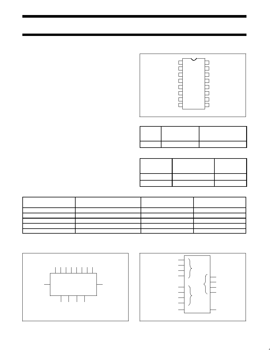
PIN CONFIGURATION
7
14
13
12
11
10
9
6
5
4
3
2
1
V
CC
B2
A3
B3
C
OUT
A0
B1
B0
1
GND
A1
0
SF00852
3
2
C
IN
A2
8
16
15
TYPE
TYPICAL
PROPAGATION
DELAY
TYPICAL
SUPPLY CURRENT
(TOTAL)
74F283
6.5ns
40mA
ORDERING INFORMATION
DESCRIPTION
COMMERCIAL RANGE
V
CC
= 5V
±
10%,
T
amb
= 0
∞
C to +70
∞
C
PKG DWG #
16-pin plastic DIP
N74F283N
SOT38-4
16-pin plastic SO
N74F283D
SOT109-1
INPUT AND OUTPUT LOADING AND FAN-OUT TABLE
PINS
DESCRIPTION
74F(U.L.)
HIGH/LOW
LOAD VALUE
HIGH/LOW
A0 - A3
A operand inputs
1.0/2.0
20
µ
A/1.2mA
B0 - B3
B operand inputs
1.0/2.0
20
µ
A/1.2mA
C
IN
Carry input
1.0/1.0
20
µ
A/0.6mA
C
OUT
Carry output
50/33
1.0mA/20mA
0≠
3
Sum outputs
50/33
1.0mA/20mA
NOTE:
One (1.0) FAST Unit Load is defined as: 20
µ
A in the High state and 0.6mA in the Low state.
LOGIC SYMBOL
5
6
3
2
14 15 12 11
4
1
1
0
A0 B0 A1 B1 A2 B2 A3 B3
SF00853
13
10
3
2
9
7
C
IN
C
OUT
V
CC
=Pin 16
GND=Pin 8
LOGIC SYMBOL (IEEE/IEC)
5
3
14
12
6
2
15
11
7
10
9
SF00854
13
1
4
CO
CI
0
3
0
3
P
Q
0
3
Philips Semiconductors
Product specification
74F283
4-bit binary full adder with fast carry
1989 Mar 03
3
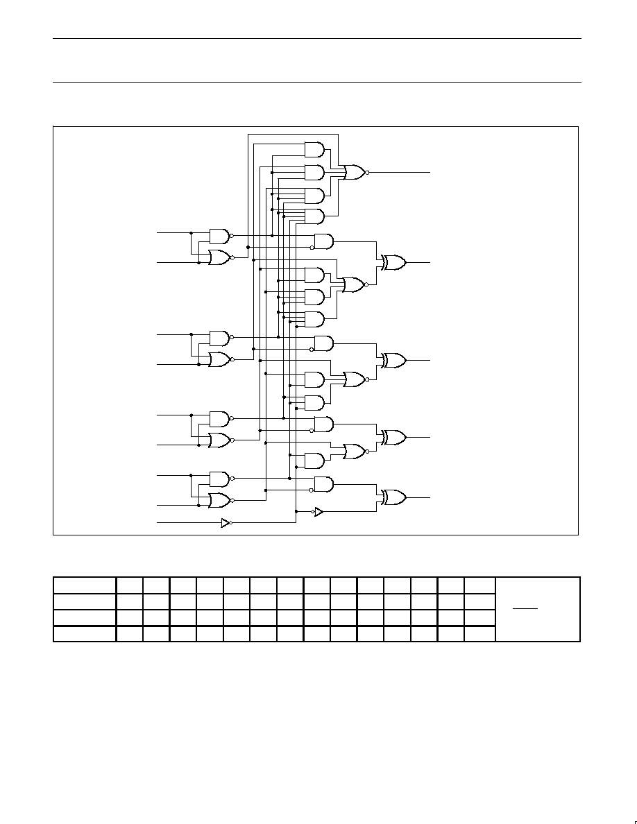
LOGIC DIAGRAM
3
9
10
13
1
4
11
12
15
14
2
3
6
5
7
B3
A3
B2
A2
B1
A1
B0
A0
C
IN
C
OUT
2
1
0
V
CC
=Pin 16
GND=Pin 8
SF00855
FUNCTION TABLE
PINS
C
IN
A0
A1
A2
A3
B0
B1
B2
B3
0
1
2
3
C
OUT
Example:
1001
Logic levels
L
L
H
L
H
H
L
L
H
H
H
L
L
H
1001
1010
10011
Active High
0
0
1
0
1
1
0
0
1
1
1
0
0
1
10011
(10+9=19)
Active Low
1
1
0
1
0
0
1
1
0
0
0
1
1
0
(10+9=19)
(carry+5+6=12)
H = High voltage level
L = Low voltage level
Philips Semiconductors
Product specification
74F283
4-bit binary full adder with fast carry
1989 Mar 03
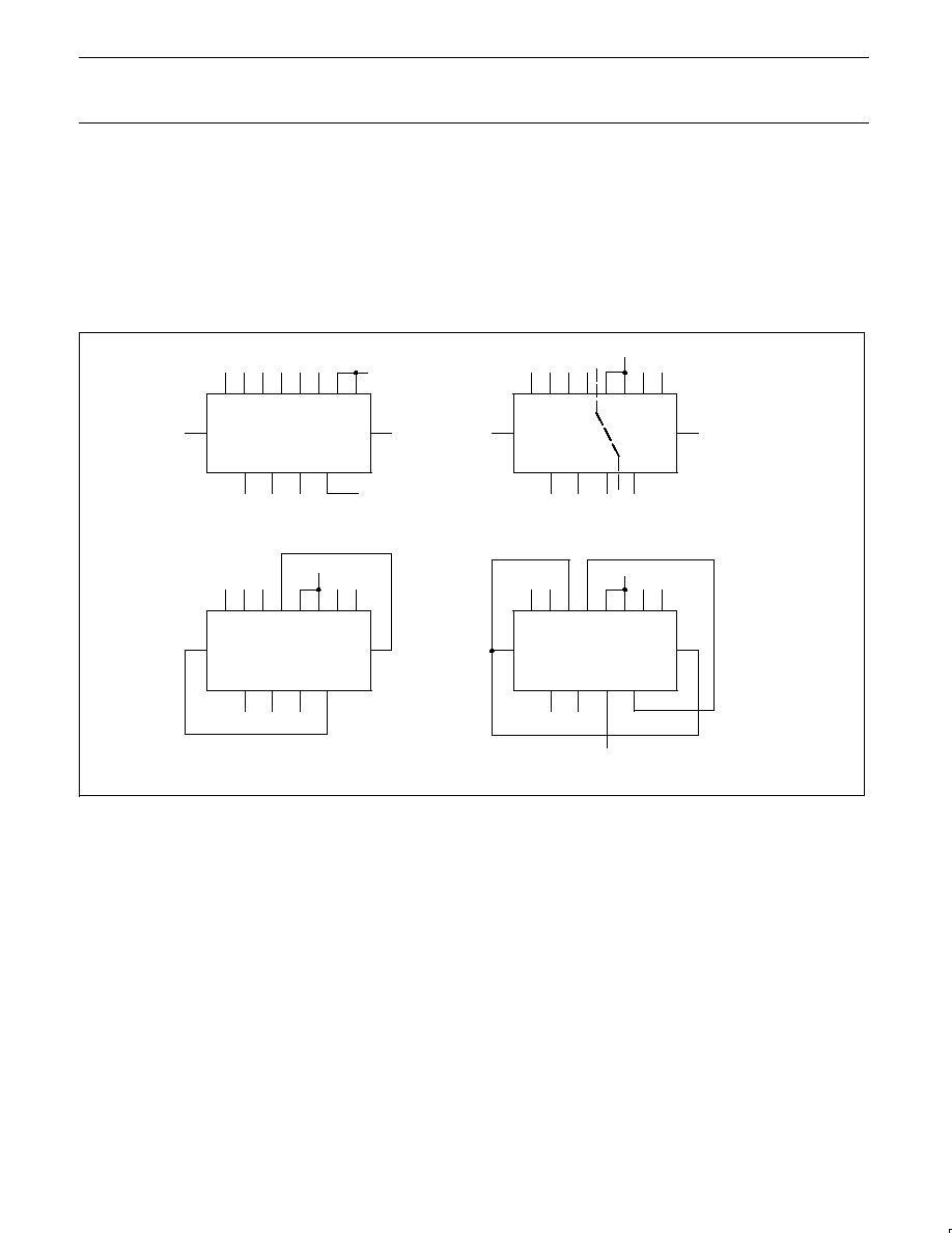
4
Figure A shows how to make a 3-bit adder. Tying the operand inputs
of the fourth adder (A3, B3) Low makes
3 dependent only on, and
equal to, the carry from the third adder. Using somewhat the same
principle, Figure B shows a way of dividing the 74F283 into a 2-bit
and a 1-bit adder. The third stage adder (A2, B2,
2) is used as
means of getting a carry (C10) signal into the fourth stage adder (via
A2 and B2) and bringing out the carry from the second stage on
2.
Note that as long as A2 and B2 are the same, whether High or Low,
they do not influence
2. Similarly, when A2 and B2 are the same,
the carry into the third stage does not influence the carry out of the
third stage. Figure C shows a method of implementing a 5-input
encoder where the inputs are equally weighted. The outputs
0,
1
and
2 present a binary number of inputs I0≠I4 that are true.
Figure D shows one method of implementing a 5-input majority gate.
When three or more of the inputs I0≠I4 are true, the output M4 is
true.
APPLICATIONS
1
0
A0 B0 A1 B1 A2 B2 A3 B3
SF00856
3
2
C
IN
C
OUT
L
C3
A.
3-bit Adder
1
0
A0 B0 A1 B1 A2 B2 A3 B3
3
2
C
IN
C
OUT
B.
2-bit and 1-bit Adder
C
IN
C
11
A0 B0 A1 B1
C10
A10 B10
1
0
10
C2
1
0
A0 B0 A1 B1 A2 B2 A3 B3
3
2
C
IN
C
OUT
C.
5-input Encoder
1
0
A0 B0 A1 B1 A2 B2 A3 B3
3
2
C
IN
C
OUT
D.
5-input Majority Gate
I0
I1
I2
I3
I4
2
0
2
1
2
2
I0
I1
I2
I3
I4
L
M4

Philips Semiconductors
Product specification
74F283
4-bit binary full adder with fast carry
1989 Mar 03
5
ABSOLUTE MAXIMUM RATINGS
(Operation beyond the limits set forth in this table may impair the useful life of the device. Unless otherwise noted these limits are over the
operating free-air temperature range.)
SYMBOL
PARAMETER
RATING
UNIT
V
CC
Supply voltage
≠0.5 to +7.0
V
V
IN
Input voltage
≠0.5 to +7.0
V
I
IN
Input current
≠30 to +5
mA
V
OUT
Voltage applied to output in High output state
≠0.5 to V
CC
V
I
OUT
Current applied to output in Low output state
40
mA
T
amb
Operating free-air temperature range
0 to +70
∞
C
T
stg
Storage temperature
≠65 to +150
∞
C
RECOMMENDED OPERATING CONDITIONS
SYMBOL
PARAMETER
LIMITS
UNIT
SYMBOL
PARAMETER
Min
Nom
Max
UNIT
V
CC
Supply voltage
4.5
5.0
5.5
V
V
IH
High-level input voltage
2.0
V
V
IL
Low-level input voltage
0.8
V
I
IK
Input clamp current
≠18
mA
I
OH
High-level output current
≠1
mA
I
OL
Low-level output current
20
mA
T
amb
Operating free-air temperature range
0
70
∞
C
DC ELECTRICAL CHARACTERISTICS
(Over recommended operating free-air temperature range unless otherwise noted.)
NO TAG
LIMITS
SYMBOL
PARAMETER
TEST CONDITIONS
NO TAG
MIN
TYP
NO TAG
MAX
UNIT
V
O
High level output voltage
V
CC
= MIN, V
IL
= MAX
±
10%V
CC
2.5
V
V
OH
High-level output voltage
V
IH
= MIN, I
OH
= MAX
±
5%V
CC
2.7
3.4
V
V
O
Low level output voltage
V
CC
= MIN, V
IL
= MAX
±
10%V
CC
0.30
0.50
V
V
OL
Low-level output voltage
V
IH
= MIN, I
OL
= MAX
±
5%V
CC
0.30
0.50
V
V
IK
Input clamp voltage
V
CC
= MIN, I
I
= I
IK
≠0.73
≠1.2
V
I
I
Input current at maximum input voltage
V
CC
= MAX, V
I
= 7.0V
100
µ
A
I
IH
High-level input current
V
CC
= MAX, V
I
= 2.7V
20
µ
A
I
Low level input current
C
IN
only
V
CC
= MAX V = 0 5V
≠0.6
mA
I
IL
Low-level input current
An, Bn
V
CC
= MAX, V
I
= 0.5V
≠1.2
mA
I
OS
Short-circuit output current
NO TAG
V
CC
= MAX
≠60
≠150
mA
I
CC
Supply current (total)
4
V
CC
= MAX
40
55
mA
NOTES:
1. For conditions shown as MIN or MAX, use the appropriate value specified under recommended operating conditions for the applicable type.
2. All typical values are at V
CC
= 5V, T
amb
= 25
∞
C.
3. Not more than one output should be shorted at a time. For testing I
OS
, the use of high-speed test apparatus and/or sample-and-hold
techniques are preferable in order to minimize internal heating and more accurately reflect operational values. Otherwise, prolonged shorting
of a High output may raise the chip temperature well above normal and thereby cause invalid readings in other parameter tests. In any
sequence of parameter tests, I
OS
tests should be performed last.
4. I
CC
should be measured with all outputs open and the following conditions:
Condition1: all inputs grounded
Condition 2: all B inputs Low, other inputs at 4.5V
Condition 3: all inputs at 4.5V