 | –≠–ª–µ–∫—Ç—Ä–æ–Ω–Ω—ã–π –∫–æ–º–ø–æ–Ω–µ–Ω—Ç: N74F299N | –°–∫–∞—á–∞—Ç—å:  PDF PDF  ZIP ZIP |
Philips
Semiconductors
74F299
8-bit universal shift/storage register
(3-State)
Product specification
IC15 Data Handbook
1990 Mar 01
INTEGRATED CIRCUITS
Philips Semiconductors
Product specification
74F299
8-bit universal shift/storage register (3-State)
2
1990 Mar 01
853-0365 98989
FEATURES
∑
Common parallel I/O for reduced pin count
∑
Additional serial inputs and outputs for expansion
∑
Four operating modes: Shift left, shift right, load and store
∑
3-State outputs for bus-oriented applications
DESCRIPTION
The 74F299 is an 8-bit universal shift/storage register with 3-State
outputs. Four modes of operation are possible: Hold (store), shift
left, shift right and parallel load. The parallel load inputs and flip-flop
outputs are multiplexed to reduce the total number of package pins.
Additional outputs are provided for flip-flops Q0 and Q7 to allow
easy serial cascading. A separate active-Low Master Reset is used
to reset the register.
The 74F299 contains eight edge-triggered D-type flip-flops and the
interstage logic necessary to perform synchronous shift left, shift
right, parallel load and hold operations. The type of operation is
determined by S0 and S1, as shown in the Function Table. All
flip-flop outputs are brought out through 3-State buffers to separate
I/O pins that also serve as data inputs in the parallel load mode.
Q0 and Q7 are also brought out on other pins for expansion in serial
shifting of longer words.
A Low signal on MR overrides the Select and CP inputs and resets
the flip-flops. All other state changes are initiated by the rising edge
of the clock. Inputs can change when the clock is in either state
provided only that the recommended setup and hold times, relative
to the rising edge of clock are observed.
A High signal on either OE0 or OE1 disables the 3-State buffers and
puts the I/O pins in the high impedance state. In this condition the
shift, hold, load and reset operations can still occur. The 3-State
buffers are also disabled by High signals on both S0 and S1 in
preparation for a parallel load operation.
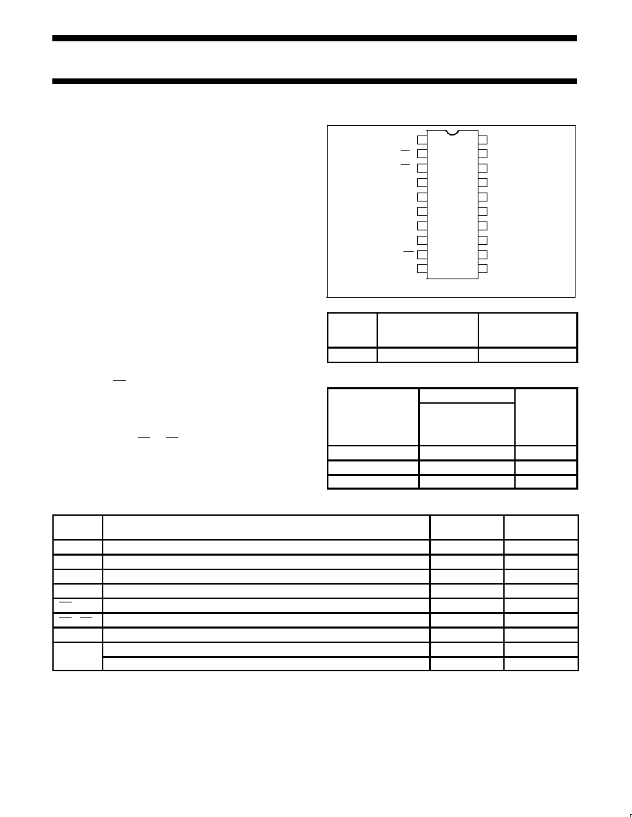
PIN CONFIGURATION
20
19
18
17
16
15
14
13
12
10
11
9
8
7
6
5
4
3
2
1
VCC
S1
DS7
Q7
I/O7
I/O5
I/O3
I/O1
DS0
S0
I/O6
I/O4
I/O2
I/O0
Q0
OE0
OE1
MR
GND
CP
SF00865
TYPE
TYPICAL f
MAX
TYPICAL
SUPPLY CURRENT
(TOTAL)
74F299
115MHz
58mA
ORDERING INFORMATION
ORDER CODE
DESCRIPTION
COMMERCIAL
RANGE
V
CC
= 5V
±
10%,
T
amb
= 0
∞
C to +70
∞
C
PKG DWG #
20-pin plastic DIP
N74F299N
SOT146-1
20-pin plastic SOL
N74F299D
SOT163-1
20-pin plastic SSOP II
N74F299DB
SOT339-1
INPUT AND OUTPUT LOADING AND FAN-OUT TABLE
PINS
DESCRIPTION
74F(U.L.)
HIGH/LOW
LOAD VALUE
HIGH/LOW
DS0
Serial data input for right shift
1.0/1.0
20
µ
A/0.6mA
DS7
Serial data input for left shift
1.0/1.0
20
µ
A/0.6mA
S0, S1
Mode select inputs
1.0/2.0
20
µ
A/1.2mA
CP
Clock pulse input (Active rising edge)
1.0/1.0
20
µ
A/0.6mA
MR
Asynchronous Master Reset input (Active Low)
1.0/1.0
20
µ
A/0.6mA
OE0, OE1
Output Enable input (Active Low)
1.0/1.0
20
µ
A/0.6mA
Q0, Q7
Serial outputs
50/33
1.0mA/20mA
I/On
Multiplexed parallel data inputs or
3.5/1.0
70
µ
A/0.6mA
I/On
3-State parallel outputs
150/40
3.0mA/24mA
NOTE: One (1.0) FAST Unit Load (U.L.) is defined as: 20
µ
A in the High State and 0.6mA in the Low state.
Philips Semiconductors
Product specification
74F299
8-bit universal shift/storage register (3-State)
1990 Mar 01
3
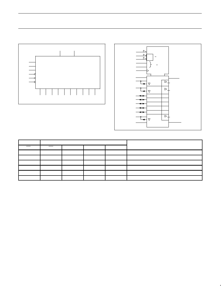
LOGIC SYMBOL
11
18
7
13
6
14
5
15
4
16
1
19
12
9
2
3
Q0
Q7
DS0
DS7
I/00
I/O2
I/O4
I/O6
I/O1
I/O3
I/O5
I/O7
S0
S1
CP
OE0
OE1
MR
VCC = Pin 20
GND = Pin 10
8
17
SF00866
LOGIC SYMBOL (IEEE/IEC)
SF00890
&
3EN13
C4/1
/2
9
4R
11
7
6
14
5
15
4
3
12
19
17
8
SRG8
1, 4D
2
1
0
3
M
0
1
3, 4D
5, 13
13
3, 4D
6, 13
3, 4D
12, 13
2, 4D
16
18
Z5
Z6
Z6
Z12
FUNCTION TABLE
INPUTS
INPUTS
OPERATING MODE
OEn
MR
S1
S0
CP
OPERATING MODE
L
L
X
X
X
Asynchronous Reset; Q0 - Q7 = Low
L
H
H
H
Parallel load; I/On
Qn (I/On outputs disabled)
L
H
L
H
Shift right; DS0
Q0, Q0
Q1, etc.
L
H
H
L
Shift left; DS7
Q7, Q7
Q6, etc.
L
H
L
L
X
Hold
H
X
X
X
X
Outputs in High Z
H = High voltage level
L = Low voltage level
X = Don't care
= Low-to-High clock transition
Philips Semiconductors
Product specification
74F299
8-bit universal shift/storage register (3-State)
1990 Mar 01
4
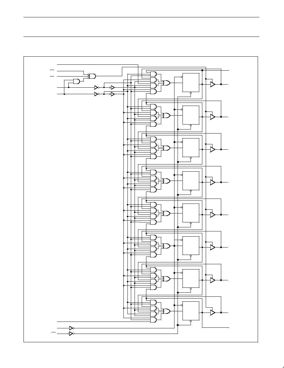
LOGIC DIAGRAM
R
D
Q
Q7
I/O7
S0
D
CP
R
D
Q
I/O6
D
CP
R
D
Q
I/O5
D
CP
R
D
Q
I/O4
D
CP
R
D
Q
I/O3
D
CP
R
D
Q
I/O2
D
CP
R
D
Q
I/O1
D
CP
R
D
Q
I/O0
D
CP
Q0
MR
CP
DS0
S1
OE1
OE0
DS7
SF00868
18
2
3
19
1
11
12
9
VCC = Pin 20
GND = Pin 10
17
16
4
15
5
14
6
13
7
8
Philips Semiconductors
Product specification
74F299
8-bit universal shift/storage register (3-State)
1990 Mar 01
5
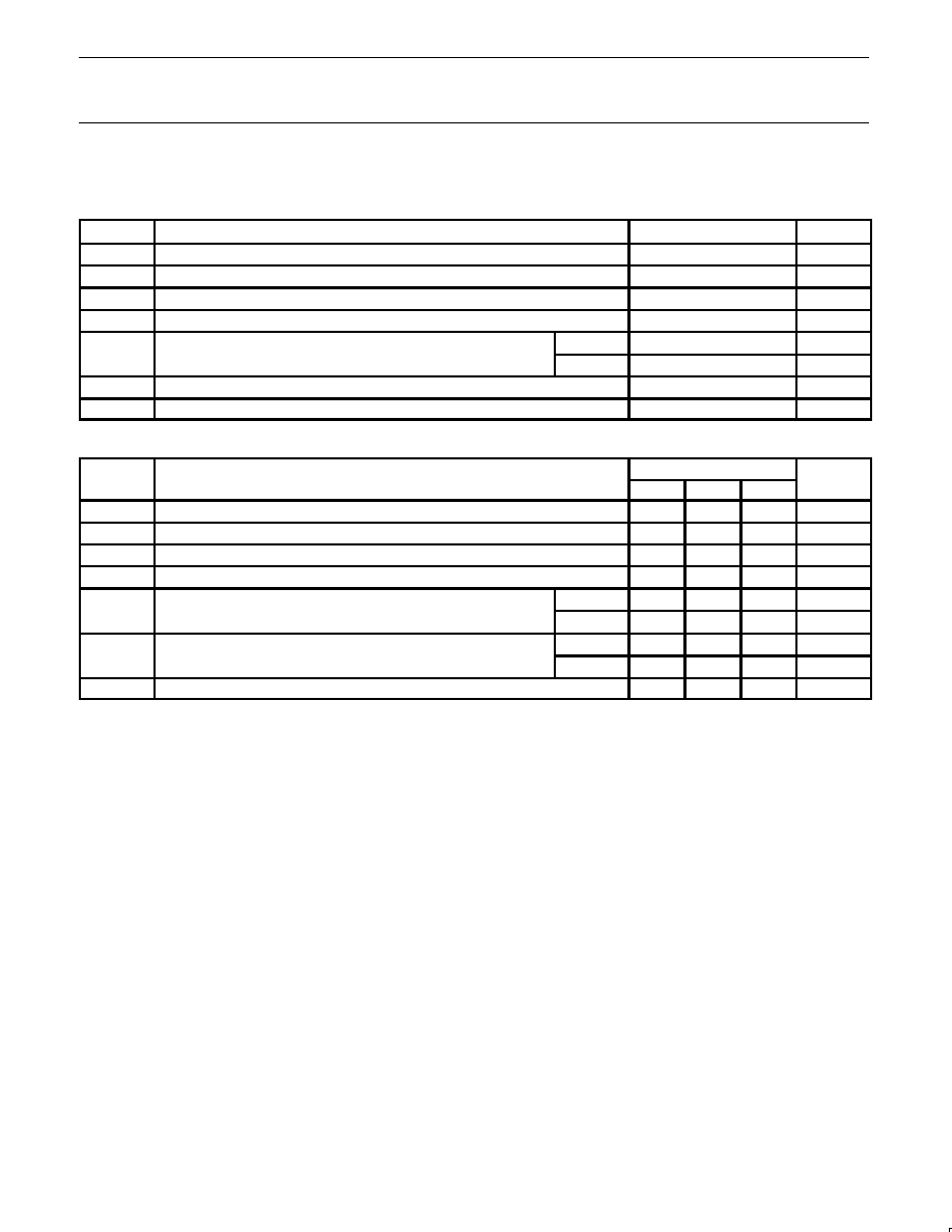
ABSOLUTE MAXIMUM RATINGS
(Operation beyond the limits set forth in this table may impair the useful life of the device. Unless otherwise noted these limits are over the
operating free-air temperature range.)
SYMBOL
PARAMETER
RATING
UNIT
V
CC
Supply voltage
≠0.5 to +7.0
V
V
IN
Input voltage
≠0.5 to +7.0
V
I
IN
Input current
≠30 to +5
mA
V
OUT
Voltage applied to output in High output state
≠0.5 to +V
CC
V
I
O
Current applied to output in Low output state
Q0, Q7
40
mA
I
OUT
Current applied to output in Low output state
I/On
48
mA
T
amb
Operating free-air temperature range
0 to +70
∞
C
T
stg
Storage temperature
≠65 to +150
∞
C
RECOMMENDED OPERATING CONDITIONS
SYMBOL
PARAMETER
LIMITS
UNIT
MIN
NOM
MAX
V
CC
Supply voltage
4.5
5.0
5.5
V
V
IH
High-level input voltage
2.0
V
V
IL
Low-level input voltage
0.8
V
I
IK
Input clamp current
≠18
mA
I
O
High level output current
Q0, Q7
≠1
mA
I
OH
High-level output current
I/On
≠3
mA
I
O
Low level output current
Q0, Q7
20
mA
I
OL
Low-level output current
I/On
24
mA
T
amb
Operating free-air temperature range
0
70
∞
C
Philips Semiconductors
Product specification
74F299
8-bit universal shift/storage register (3-State)
1990 Mar 01
6
DC ELECTRICAL CHARACTERISTICS
(Over recommended operating free-air temperature range unless otherwise noted.)
NO TAG
LIMITS
SYMBOL
PARAMETER
TEST CONDITIONS
NO TAG
MIN
TYP
NO TAG
MAX
UNIT
Q0 Q7
I
O
= 1mA
±
10%V
CC
2.5
V
V
O
High level output voltage
Q0, Q7
V
CC
= MIN,
V
MAX
I
OH
= ≠1mA
±
5%V
CC
2.7
3.4
V
V
OH
High-level output voltage
I/On
V
IL
= MAX,
V
IH
= MIN
I
O
= 3mA
±
10%V
CC
2.4
V
I/On
IH
I
OH
= ≠3mA
±
5%V
CC
2.7
3.3
V
V
O
Low level output voltage
V
CC
= MIN,
V
MAX
I
O
= MAX
±
10%V
CC
0.35
0.50
V
V
OL
Low-level output voltage
V
IL
= MAX,
V
IH
= MIN
I
OL
= MAX
±
5%V
CC
0.35
0.50
V
V
IK
Input clamp voltage
V
CC
= MIN, I
I
= I
IK
≠0.73
≠1.2
V
I
I
Input current at
others
V
CC
= MAX, V
I
= 7.0V
100
µ
A
In ut current at
maximum input voltage
I/On
V
CC
= 5.5V, V
I
= 5.5V
1
mA
I
IH
High-level input current
except
I/On
V
CC
= MAX, V
I
= 2.7V
20
µ
A
I
Low level input current
S0, S1
V
CC
= MAX V = 0 5V
≠1.2
mA
I
IL
Low-level input current
others
V
CC
= MAX, V
I
= 0.5V
≠0.6
mA
I
IH +
I
OZH
Off-state output current,
High-level voltage
applied
I/On
only
V
CC
= MAX, V
O
= 2.7V
70
µ
A
I
IL +
I
OZL
Off-state output current
Low-level voltage applied
only
V
CC
= MAX, V
O
= 0.5V
≠0.6
mA
I
OS
Short-circuit output current
NO TAG
V
CC
= MAX
≠60
≠150
mA
I
CCH
55
60
mA
I
CC
Supply current (total)
I
CCL
V
CC
= MAX
70
90
mA
I
CCZ
65
95
mA
NOTES:
1. For conditions shown as MIN or MAX, use the appropriate value specified under recommended operating conditions for the applicable type.
2. All typical values are at V
CC
= 5V, T
amb
= 25
∞
C.
3. Not more than one output should be shorted at a time. For testing I
OS
, the use of high-speed test apparatus and/or sample-and-hold
techniques are preferable in order to minimize internal heating and more accurately reflect operational values. Otherwise, prolonged shorting
of a High output may raise the chip temperature well above normal and thereby cause invalid readings in other parameter tests. In any
sequence of parameter tests, I
OS
tests should be performed last.
Philips Semiconductors
Product specification
74F299
8-bit universal shift/storage register (3-State)
1990 Mar 01
7
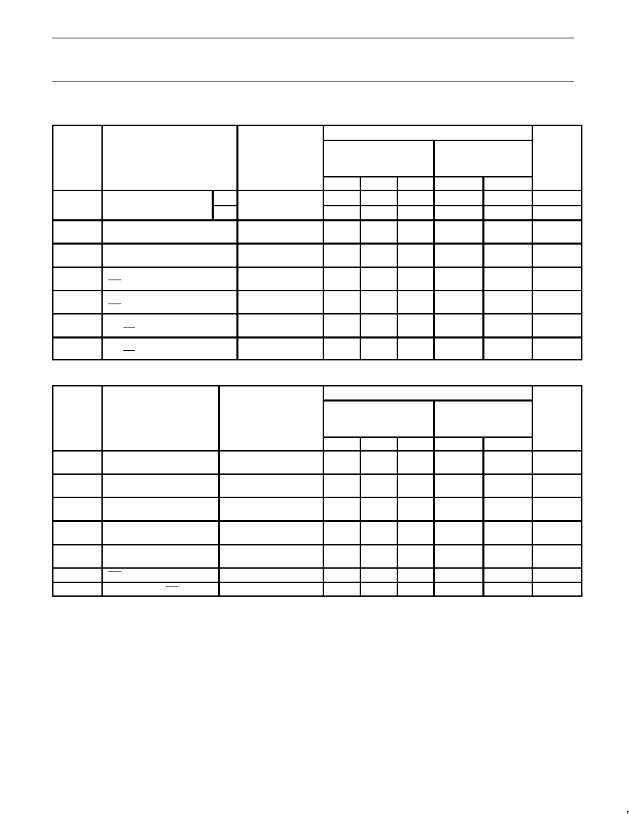
AC ELECTRICAL CHARACTERISTICS
LIMITS
T
amb
= +25
∞
C
T
amb
= 0
∞
C to +70
∞
C
SYMBOL
PARAMETER
TEST CONDITIONS
V
CC
= +5.0V
V
CC
= +5.0V
±
10%
UNIT
C
L
= 50pF, R
L
= 500
C
L
= 50pF, R
L
= 500
MIN
TYP
MAX
MIN
MAX
f
Maximum clock frequency
I/O
Waveform 1
70
100
70
MHz
f
MAX
Maximum clock frequency
Qn
Waveform 1
85
115
85
MHz
t
PLH
t
PHL
Propagation delay
CP to Q0 or Q7
Waveform 1
4.0
4.5
5.0
6.0
7.5
8.0
3.5
4.5
8.5
8.5
ns
ns
t
PLH
t
PHL
Propagation delay
CP to I/On
Waveform 1
4.0
4.0
6.0
6.5
9.0
9.0
4.0
4.0
10.0
10.0
ns
ns
t
PHL
Propagation delay
MR to Q0 or Q7
Waveform 2
5.5
7.5
9.5
5.5
10.5
ns
t
PHL
Propagation delay
MR to I/On
Waveform 2
5.5
7.5
10.0
5.5
10.5
ns
t
PZH
t
PZL
Output Enable time
Sn, OE to I/On
Waveform 4
Waveform 5
3.5
4.0
6.0
7.5
8.0
10.0
3.5
4.0
9.0
11.0
ns
ns
t
PHZ
t
PLZ
Output Disable time
Sn, OE to I/On
Waveform 4
Waveform 5
2.5
1.5
4.5
2.5
7.0
5.5
2.5
1.5
8.0
6.5
ns
ns
AC SETUP REQUIREMENTS
LIMITS
T
amb
= +25
∞
C
T
amb
= 0
∞
C to +70
∞
C
SYMBOL
PARAMETER
TEST CONDITIONS
V
CC
= +5.0V
V
CC
= +5.0V
±
10%
UNIT
C
L
= 50pF, R
L
= 500
C
L
= 50pF, R
L
= 500
MIN
TYP
MAX
MIN
MAX
t
s
(H)
t
s
(L)
Setup time, High or Low
S0 or S1 to CP
Waveform 3
6.5
6.5
7.5
7.5
ns
ns
t
h
(H)
t
h
(L)
Hold time, High or Low
S0 or S1 to CP
Waveform 3
0
0
0
0
ns
ns
t
s
(H)
t
s
(L)
Set-up time, High or Low
I/On, DS
L
or DS
R
to CP
Waveform 3
3.5
3.5
4.0
4.0
ns
ns
t
h
(H)
t
h
(L)
Hold time, High or Low
I/On, DS
L
or DS
R
to CP
Waveform 3
0
0
0
0
ns
ns
t
w
(H)
t
w
(L)
CP Pulse width, High or Low
Waveform 1
5.0
4.5
5.0
4.5
ns
t
w
(L)
MR Pulse width, Low
Waveform 2
4.5
4.5
ns
t
rec
Recovery time, MR to CP
Waveform 2
4.0
4.0
ns
Philips Semiconductors
Product specification
74F299
8-bit universal shift/storage register (3-State)
1990 Mar 01
8
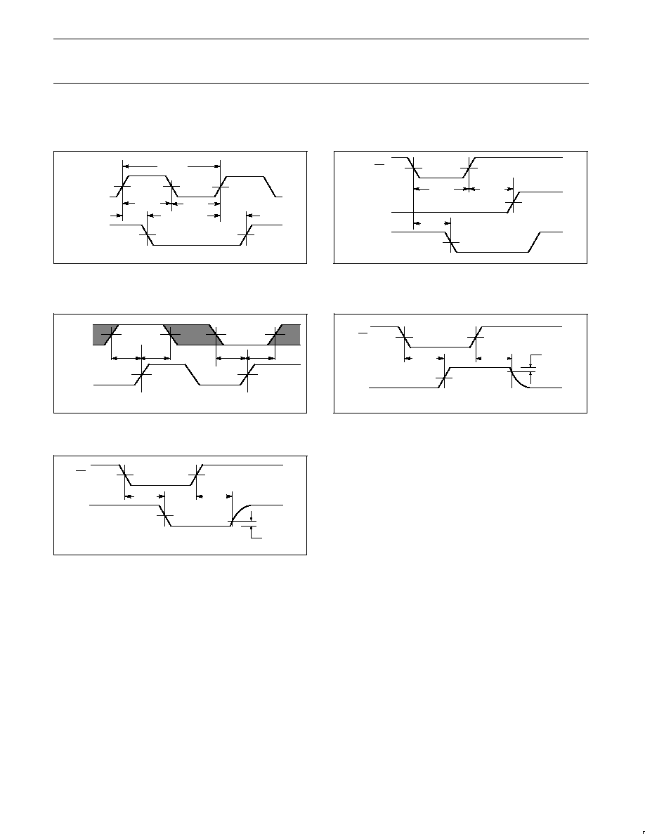
AC WAVEFORMS
For all waveforms, V
M
= 1.5V
The shaded areas indicate when the input is permitted to change for predictable output performance.
VM
tPLH
tPHL
VM
VM
VM
1/fMAX
tW(L)
CP
Q0, Q7, I/On
tW(H)
SF00869
Waveform 1. Propagation Delay, Clock Input to Output,
Clock Width, and Maximum Clock Frequency
VM
VM
VM
tPHL
tW(L)
tREC
VM
Q0, Q7, I/On
CP
MR
SF00870
Waveform 2. Master Reset Pulse Width, Master Reset to Output
Delay, and Master Reset to Clock Recovery Time
VM
VM
VM
VM
VM
VM
S0, S1,
I/On
DS
L
,
DS
R
CP
SF00871
ts(H)
th(H)
th(L)
ts(L)
Waveform 3. Setup and Hold Times
VM
VM
VM
tPHZ
tPZH
Sn, OEn
I/On
VOH -0.3V
0V
SF00872
Waveform 4. 3-State Output Enable Time to High Level
and Output Disable Time from High Level
VM
VM
VM
tPLZ
tPZL
Sn, OEn
I/On
VOL +0.3V
SF00873
Waveform 5. 3-State Output Enable Time to Low Level and
Output Disable Time from Low Level
Philips Semiconductors
Product specification
74F299
8-bit universal shift/storage register (3-State)
1990 Mar 01
9
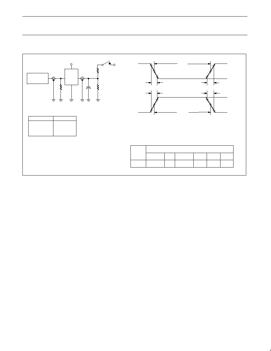
TEST CIRCUIT AND WAVEFORM
tw
90%
VM
10%
90%
VM
10%
90%
VM
10%
90%
VM
10%
NEGATIVE
PULSE
POSITIVE
PULSE
tw
AMP (V)
0V
0V
tTHL (tf
)
INPUT PULSE REQUIREMENTS
rep. rate
t
w
t
TLH
t
THL
1MHz
500ns
2.5ns
2.5ns
Input Pulse Definition
VCC
family
74F
D.U.T.
PULSE
GENERATOR
RL
CL
RT
VIN
VOUT
Test Circuit for 3-State Outputs
DEFINITIONS:
R
L
= Load resistor;
see AC electrical characteristics for value.
C
L
= Load capacitance includes jig and probe capacitance;
see AC electrical characteristics for value.
R
T
= Termination resistance should be equal to Z
OUT
of
pulse generators.
tTHL (tf
)
tTLH (tr
)
tTLH (tr
)
AMP (V)
amplitude
3.0V
1.5V
V
M
RL
7.0V
SF00777
TEST
SWITCH
t
PLZ
closed
t
PZL
closed
All other
open
SWITCH POSITION
Philips Semiconductors
Product specification
74F299
8-bit universal shift/storage register (3-State)
1990 Mar 01
10
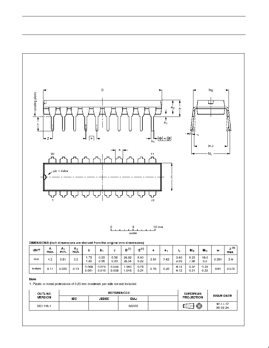
DIP20:
plastic dual in-line package; 20 leads (300 mil)
SOT146-1
Philips Semiconductors
Product specification
74F299
8-bit universal shift/storage register (3-State)
1990 Mar 01
11
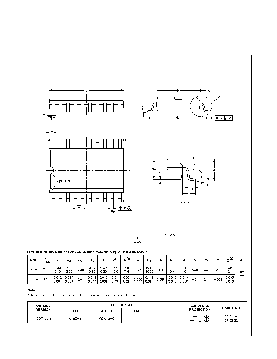
SO20:
plastic small outline package; 20 leads; body width 7.5 mm
SOT163-1
Philips Semiconductors
Product specification
74F299
8-bit universal shift/storage register (3-State)
1990 Mar 01
12
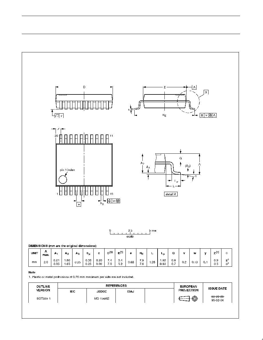
SSOP20:
plastic shrink small outline package; 20 leads; body width 5.3 mm
SOT339-1

Philips Semiconductors
Product specification
74F299
8-bit universal shift/storage register (3-State)
1990 Mar 01
13
NOTES
Philips Semiconductors
Product specification
74F299
8-bit universal shift/storage register (3-State)
yyyy mmm dd
14
Definitions
Short-form specification -- The data in a short-form specification is extracted from a full data sheet with the same type number and title. For
detailed information see the relevant data sheet or data handbook.
Limiting values definition -- Limiting values given are in accordance with the Absolute Maximum Rating System (IEC 134). Stress above one
or more of the limiting values may cause permanent damage to the device. These are stress ratings only and operation of the device at these or
at any other conditions above those given in the Characteristics sections of the specification is not implied. Exposure to limiting values for extended
periods may affect device reliability.
Application information -- Applications that are described herein for any of these products are for illustrative purposes only. Philips
Semiconductors make no representation or warranty that such applications will be suitable for the specified use without further testing or
modification.
Disclaimers
Life support -- These products are not designed for use in life support appliances, devices or systems where malfunction of these products can
reasonably be expected to result in personal injury. Philips Semiconductors customers using or selling these products for use in such applications
do so at their own risk and agree to fully indemnify Philips Semiconductors for any damages resulting from such application.
Right to make changes -- Philips Semiconductors reserves the right to make changes, without notice, in the products, including circuits, standard
cells, and/or software, described or contained herein in order to improve design and/or performance. Philips Semiconductors assumes no
responsibility or liability for the use of any of these products, conveys no license or title under any patent, copyright, or mask work right to these
products, and makes no representations or warranties that these products are free from patent, copyright, or mask work right infringement, unless
otherwise specified.
Philips Semiconductors
811 East Arques Avenue
P.O. Box 3409
Sunnyvale, California 94088≠3409
Telephone 800-234-7381
©
Copyright Philips Electronics North America Corporation 1998
All rights reserved. Printed in U.S.A.
print code
Date of release: 10-98
Document order number:
9397-750-05117
Philips
Semiconductors
Data sheet
status
Objective
specification
Preliminary
specification
Product
specification
Product
status
Development
Qualification
Production
Definition
[1]
This data sheet contains the design target or goal specifications for product development.
Specification may change in any manner without notice.
This data sheet contains preliminary data, and supplementary data will be published at a later date.
Philips Semiconductors reserves the right to make chages at any time without notice in order to
improve design and supply the best possible product.
This data sheet contains final specifications. Philips Semiconductors reserves the right to make
changes at any time without notice in order to improve design and supply the best possible product.
Data sheet status
[1]
Please consult the most recently issued datasheet before initiating or completing a design.