Philips Semiconductors
Product specification
74F30240*, 74F30244
30
line drivers
74F30240
Octal 30
line driver with enable, inverting (open collector)
74F30244
Octal 30
line driver with enable, non-inverting (open collecor)
2
1999 Jan 08
853≠1157 20619
* Discontinued part. Please see the Discontinued Products List.
FEATURES
∑
Ideal for driving transmission lines or backplanes. 160mA I
OL
ideal
for applications with impedance as low as 30
∑
Guaranteed threshold voltages on the incident wave while driving
line as low as 30
∑
High impedance NPN base inputs for reduced loading (20
µ
A in
High and Low states)
∑
Ideal for applications which require high output drive and minimal
bus loading
∑
Octal interface
∑
74F30240 inverting
∑
74F30244 non-inverting
∑
Open-Collector outputs sink 160mA
∑
Multiple side pins are used for V
CC
and GND to reduce lead
inductance (improves speed and noise immunity)
∑
Available in 24-pin standard slim DIP (300mil) plastic, SOL or
CERDIP packages
DESCRIPTION
The 74F30240 and 74F30244 are high current open collector octal
buffers composed of eight inverters. The 74F30240 has inverting
data paths and the 74F30244 has non-inverting paths. Each device
has eight inverters with two Output Enables (OE0, OE1), each
controlling four outputs. Both drivers are designed to deal with the
low-impedance transmission line effects found on printed circuit
boards when fast edge rates are used. The 160mA I
OL
provides
ample power to achieve TTL switching voltages on the incident
wave.
TYPE
TYPICAL
PROPAGATION
DELAY
TYPICAL
SUPPLY CURRENT
(TOTAL)
74F30240
9.5ns
62.5mA
74F30244
10.5ns
69mA
ORDERING INFORMATION
DESCRIPTION
COMMERCIAL RANGE
V
CC
= 5V
±
10%,
T
amb
= 0
∞
C to +70
∞
C
PACKAGE
DRAWING NUMBER
24-pin Plastic Slim DIP (300mil)
N74F30244N
SOT222-1
24≠pin Plastic SOL
1
N74F30244D
SOT137-1
NOTE:
1. Because of the high current sinking capability of these parts, the SOL package should only be used under the following conditions:
a. 50% duty cycle,
AND
b. 3/5 of remaining 50% driving
100mA (leaving the remaining 2/5 of the drive
160mA)
OR
c. use
450 linear feet per minute forced air or other thermal mounting techniques.
INPUT AND OUTPUT LOADING AND FAN-OUT TABLE
PINS
DESCRIPTION
74F(U.L.)
HIGH/LOW
LOAD VALUE
HIGH/LOW
D0≠D7
Data inputs
1.0/0.033
20
µ
A/20
µ
A
OE0≠OE1
Output Enable inputs (Active Low)
1.0/0.033
20
µ
A/20
µ
A
Q0≠Q7
Data outputs (OC) for 74F30240
OC/266.7
OC/160mA
Q0≠Q7
Data outputs (OC) for 74F30244
OC/266.7
OC/160mA
NOTE: One (1.0) FAST unit load is defined as: 20
µ
A in the High state and 0.6mA in the Low state. OC = Open Collector.

Philips Semiconductors
Product specification
74F30240*, 74F30244
30
line drivers
1999 Jan 08
3
* Discontinued part. Please see the Discontinued Products List.
PIN CONFIGURATION ≠ 74F30240
1
2
3
4
5
6
7
8
9
10
11
12
13
14
15
16
17
18
19
20
21
22
23
24
Q0
Q1
Q2
Q3
GND
GND
GND
GND
Q4
Q5
Q6
D0
D1
D2
D3
OE0
V
CC
V
CC
D4
OE1
D5
D6
D7
Q7
SF01387
PIN CONFIGURATION ≠ 74F30244
1
2
3
4
5
6
7
8
9
10
11
12
13
14
15
16
17
18
19
20
21
22
23
24
Q0
Q1
Q2
Q3
GND
GND
GND
GND
Q4
Q5
Q6
D0
D1
D2
D3
OE0
V
CC
V
CC
D4
OE1
D5
D6
D7
Q7
SF01388
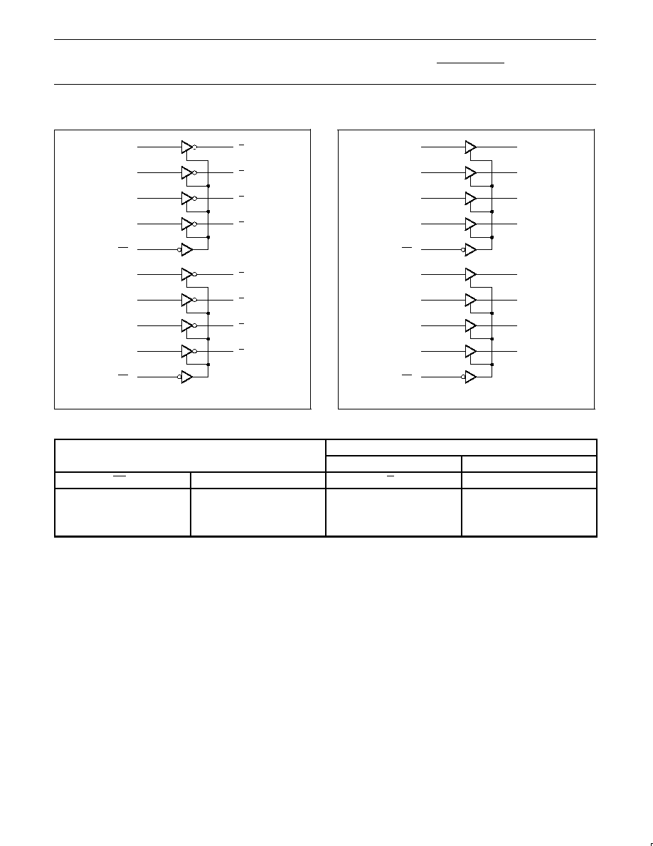
LOGIC SYMBOL ≠ 74F30240
D0 D1 D2 D3 D4 D5 D6 D7
Q0 Q1 Q2 Q3 Q4 Q5 Q6 Q7
20
OE0
17
OE1
24
23
22
21
16
15
14
13
1
2
3
4
9
10
11
12
V
CC
= PIN 18, 19
GND = PIN 5, 6, 7, 8
SF01389
LOGIC SYMBOL ≠ 74F30244
D0 D1 D2 D3 D4 D5 D6 D7
Q0 Q1 Q2 Q3 Q4 Q5 Q6 Q7
20
OE0
17
OE1
24
23
22
21
16
15
14
13
1
2
3
4
9
10
11
12
V
CC
= PIN 18, 19
GND = PIN 5, 6, 7, 8
SF01390
IEC/IEEE SYMBOL ≠ 74F30240
1
24
2
23
3
22
4
21
9
16
10
15
11
14
12
13
1
20
17
EN1
EN2
SF01391
IEC/IEEE SYMBOL ≠ 74F30244
1
24
2
23
3
22
4
21
9
16
10
15
11
14
12
13
1
20
17
EN1
EN2
SF01392
Philips Semiconductors
Product specification
74F30240*, 74F30244
30
line drivers
1999 Jan 08
5
* Discontinued part. Please see the Discontinued Products List.
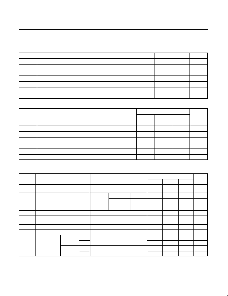
ABSOLUTE MAXIMUM RATINGS
(Operation beyond the limits set forth in this table may impair the useful life of the device.
Unless otherwise noted these limits are over the operating free-air temperature range.)
SYMBOL
PARAMETER
RATING
UNIT
V
CC
Supply voltage
≠0.5 to +7.0
V
V
IN
Input voltage
≠0.5 to +7.0
V
I
IN
Input current
≠30 to +5
mA
V
OUT
Voltage applied to output in High output state
≠0.5 to V
CC
V
I
OUT
Current applied to output in Low output state
320
mA
T
amb
Operating free-air temperature range
0 to +70
∞
C
T
stg
Storage temperature range
≠65 to +150
∞
C
RECOMMENDED OPERATING CONDITIONS
SYMBOL
PARAMETER
LIMITS
UNIT
SYMBOL
PARAMETER
MIN
NOM
MAX
UNIT
V
CC
Supply voltage
4.5
5.0
5.5
V
V
IH
High-level input voltage
2.0
V
V
IL
Low-level input voltage
0.8
V
I
IK
Input clamp current
≠18
mA
V
OH
High-level output voltage
4.5
V
I
OL
Low-level output current
160
mA
T
amb
Operating free-air temperature range
0
+70
∞
C
DC ELECTRICAL CHARACTERISTICS
(Over recommended operating free-air temperature range unless otherwise noted.)
SYMBOL
PARAMETER
TEST CONDITIONS
1
LIMITS
UNIT
SYMBOL
PARAMETER
TEST CONDITIONS
1
MIN
TYP
2
MAX
UNIT
I
OH
High-level output current
V
CC
= MIN, V
IL
= MAX,
V
IH
= MIN, V
OH
= MAX
250
µ
A
V
CC
= MIN
I
OL
= 100mA
±
10% V
CC
0.42
0.55
V
V
OL
Low-level output current
V
CC
= MIN,
V
IL
= MAX,
V
IH
= MIN
I
OL
=
160mA
NO TAG
±
5% V
CC
0.80
V
V
IK
Input clamp voltage
V
CC
= MIN, I
I
= I
IK
≠0.73
≠1.2
V
I
I
Input current at maximum
input voltage
V
CC
= 0.0V, V
I
= 7.0V
100
µ
A
I
IH
High-level input current
V
CC
= MAX, V
I
= 2.7V
20
µ
A
I
IL
Low-level input current
V
CC
= MAX, V
I
= 0.5V
≠20
µ
A
74F30240
I
CCH
V
CC
= MAX
13
23
mA
I
CC
Supply current
74F30240
I
CCL
V
CC
= MAX
70
95
mA
I
CC
y
(total)
74F30244
I
CCH
V
CC
= MAX
19
27
mA
74F30244
I
CCL
V
CC
= MAX
70
100
mA
NOTES:
1. For conditions shown as MIN or MAX, use the appropriate value specified under recommended operating conditions for the applicable type.
2. All typical values are at V
CC
= 5V, T
amb
= 25
∞
C.
3. I
OL1
is the current necessary to guarantee the High-to-Low transition in a 30
transmission line on the incident wave.