 | –≠–ª–µ–∫—Ç—Ä–æ–Ω–Ω—ã–π –∫–æ–º–ø–æ–Ω–µ–Ω—Ç: N74F322N | –°–∫–∞—á–∞—Ç—å:  PDF PDF  ZIP ZIP |
Document Outline
- FEATURES
- DESCRIPTION
- PIN CONFIGURATION
- ORDERING INFORMATION
- INPUT AND OUTPUT LOADING AND FAN-OUT TABLE
- LOGIC SYMBOL
- LOGIC SYMBOL (IEEE/IEC)
- FUNCTION TABLE
- LOGIC DIAGRAM
- ABSOLUTE MAXIMUM RATINGS
- RECOMMENDED OPERATING CONDITIONS
- DC ELECTRICAL CHARACTERISTICS
- AC ELECTRICAL CHARACTERISTICS
- AC SETUP REQUIREMENTS
- AC WAVEFORMS
- TEST CIRCUIT AND WAVEFORM
Philips Semiconductors
Product specification
74F322
8-bit serial/parallel register with sign extend (3-State)
1
1988 Apr 22
853-0366 93020
FEATURES
∑
Multiplexed parallel I/O ports
∑
Separate serial input and output
∑
Sign extend function
∑
3-State outputs for bus applications
∑
Direct Overriding Clear
DESCRIPTION
The 74F322 is an 8-bit shift register with provision for either serial or
parallel loading and with 3-State parallel outputs plus a bi-state
serial output. Parallel data inputs and outputs are multiplexed to
minimize pin count. State changes are initiated by the rising edge of
the clock. Four synchronous modes of operation are possible: hold
(store), shift right with serial entry, shift right with sign extend, and
parallel load. An asynchronous Master Reset (MR) input overrides
clocked operation and clears the registers.
The 74F322 contains eight D-type edge triggered flip-flops and the
interstage gating required to perform right shift and the intrastage
gating necessary for hold and synchronous parallel load operations.
A Low signal on RE enables shifting or parallel loading, while a High
signal enables the hold mode. A High signal on S/P enables shift
right, while a Low signal disables the 3-State output buffers and
enables parallel loading. In the shift right mode a High signal on SE
enables serial entry from either D0 or D1, as determined by the S
input. A Low signal on SE enables shift right, but Q7 reloads its
contents, thus performing the sign extend function. A High signal on
OE disables the 3-State output buffers, regardless of the other
control inputs. In this condition the shifting and loading operations
can still be performed.
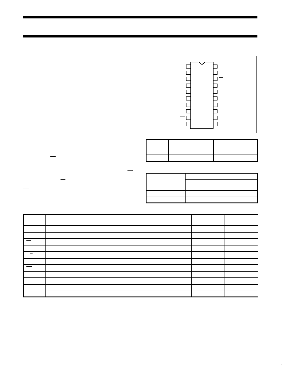
PIN CONFIGURATION
20
19
18
17
16
15
14
13
12
10
11
9
8
7
6
5
4
3
2
1
VCC
S
SE
D1
I/O7
I/O5
I/O3
I/O1
CP
RE
I/O6
I/O4
I/O2
I/O0
OE
S/P
D0
MR
GND
Q7
SF00874
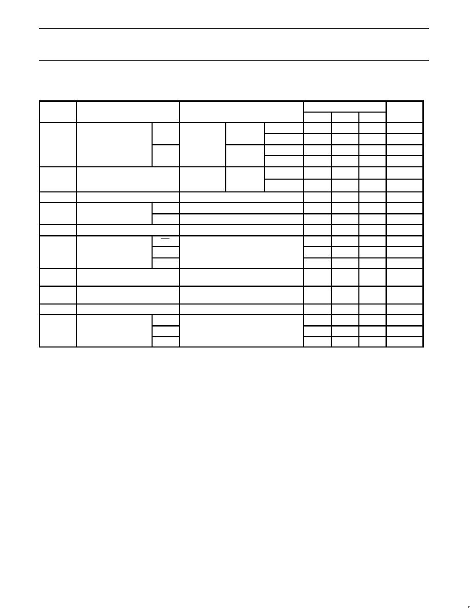
TYPE
TYPICAL f
MAX
TYPICAL
SUPPLY CURRENT
(TOTAL)
74F322
125MHz
60mA
ORDERING INFORMATION
DESCRIPTION
ORDER CODE
DESCRIPTION
COMMERCIAL RANGE
V
CC
= 5V
±
10%, T
amb
= 0
∞
C to +70
∞
C
20-pin plastic DIP
N74F322N
20-pin plastic SOL
N74F322D
INPUT AND OUTPUT LOADING AND FAN-OUT TABLE
PINS
DESCRIPTION
74F(U.L.)
HIGH/LOW
LOAD VALUE
HIGH/LOW
D0, D1
Serial data inputs
1.0/1.0
20
µ
A/0.6mA
S
Serial data select input
1.0/2.0
20
µ
A/1.2mA
SE
Sign Extend input
1.0/3.0
20
µ
A/1.8mA
CP
Clock Pulse input (Active rising edge)
1.0/1.0
20
µ
A/0.6mA
S/P
Serial (High) or Parallel (Low) mode control input
1.0/1.0
20
µ
A/0.6mA
RE
Register Enable input (Active Low)
1.0/1.0
20
µ
A/0.6mA
MR
Asynchronous Master Reset input (Active Low)
1.0/1.0
20
µ
A/0.6mA
OE
Output Enable input (Active Low)
1.0/1.0
20
µ
A/0.6mA
Q7
Bi-state serial output
50/33
1.0mA/20mA
I/On
Multiplexed parallel data inputs or
3.5/1.0
70
µ
A/0.6mA
I/On
3-State parallel outputs
150/40
3.0mA/24mA
NOTE: One (1.0) FAST Unit Load (U.L.) is defined as: 20
µ
A in the High State and 0.6mA in the Low state.
Philips Semiconductors
Product specification
74F322
8-bit serial/parallel register with sign extend (3-State)
1988 Apr 22
2
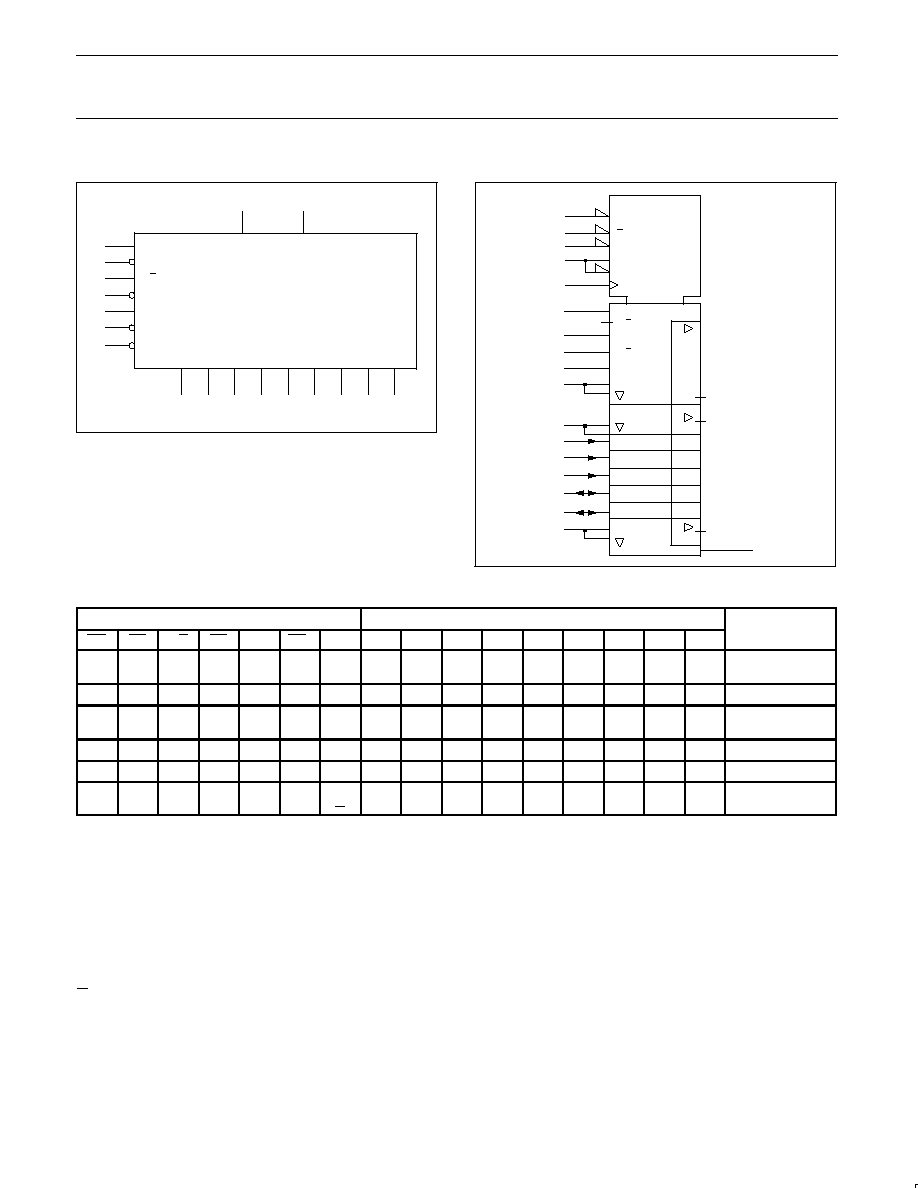
LOGIC SYMBOL
3
17
4
16
5
15
6
14
7
13
19
1
2
18
11
8
Q7
D0
D1
I/O0
I/O2
I/O4
I/O6
I/O1
I/O3
I/O5
I/O7
S
RE
S/P
CP
OE
SE
VCC = Pin 20
GND = Pin 10
12
SF00875
9
MR
LOGIC SYMBOL (IEEE/IEC)
SF00876
2EN15
C6/1
9
R
18
16
5
15
6
14
1
11
12
SRG8
G4
8
2
8, 4, 1, 6D
19
2, 6D
12, 13
7
13
Z7
Z14
G3
3M1[SHIFT]
3M2[PAR LOAD]
2, 96D
8, 15
Z8
G5
8, 5, 1, 6D
8, 4, 1, 6D
2, 6D
7, 15
4
3
17
FUNCTION TABLE
INPUTS
INPUTS
OPERATING
MODE
MR
RE
S/P
SE
S
OE*
CP
I/O0
I/O1
I/O2
I/O3
I/O4
I/O5
I/O6
I/O7
Q7
OPERATING
MODE
L
L
H
X
X
H
X
X
X
X
L
L
X
X
L
L
L
L
L
L
L
L
L
L
L
L
L
L
L
L
L
L
Clear
H
L
L
X
X
X
I0
I1
I2
I3
I4
I5
I6
I7
I7
Parallel load
H
H
L
L
H
H
H
H
L
H
L
L
D0
D1
O0
O0
O1
O1
O2
O2
O3
O3
O4
O4
O5
O5
O6
O6
O6
O6
Shift right
H
L
H
L
X
L
O0
O0
O1
O2
O3
O4
O5
O6
O6
Sign extend
H
H
X
X
X
L
X
NC
NC
NC
NC
NC
NC
NC
NC
NC
Hold
X
X
L
X
L
X
X
X
X
X
X
H
X
Z
Z
Z
Z
Z
Z
Z
Z
Z
Z
Z
Z
Z
Z
Z
Z
NC
NC
3-State
*
= When the input is High, all I/O terminals are at the high impedance state, sequential operation or clearing of the register is not
affected.
H
= High voltage level
L
= Low voltage level
NC
= No change
X
= Don't care
Z
= High impedance "off" state
= Low-to-High clock transition
I0≠I7
= The level of the steady state input at the respective I/O terminal is loaded into the flip-flop while the flip-flop outputs (except Q7) are
isolated from the I/O terminal.
D0≠D7 = The level of the steady state inputs to the serial multiplexer input.
O0≠O7 = The level of the respective Qn flip-flop prior to the last clock Low-to-High transition.
= Not a Low-to-High clock transition
Philips Semiconductors
Product specification
74F322
8-bit serial/parallel register with sign extend (3-State)
1988 Apr 22
3
LOGIC DIAGRAM
R
Q
I/O0
D1
D
CP
MR
CP
S/P
RE
OE
SF00877
11
9
VCC = Pin 20
GND = Pin 10
Q
R
Q
I/O1
D
CP
Q
R
Q
I/O2
D
CP
Q
R
Q
I/O3
D
CP
Q
R
Q
I/O4
D
CP
Q
R
Q
I/O5
D
CP
Q
R
Q
I/O6
D
CP
Q
R
Q
Q7
I/O7
D
CP
Q
S
D0
SE
8
1
2
17
19
3
18
4
16
5
15
6
14
7
12
13
Philips Semiconductors
Product specification
74F322
8-bit serial/parallel register with sign extend (3-State)
1988 Apr 22
4
ABSOLUTE MAXIMUM RATINGS
(Operation beyond the limits set forth in this table may impair the useful life of the device. Unless otherwise noted these limits are over the
operating free-air temperature range.)
SYMBOL
PARAMETER
RATING
UNIT
V
CC
Supply voltage
≠0.5 to +7.0
V
V
IN
Input voltage
≠0.5 to +7.0
V
I
IN
Input current
≠30 to +5
mA
V
OUT
Voltage applied to output in High output state
≠0.5 to +5.5
V
I
OUT
Current applied to output in Low output state
Q7
40
mA
I
OUT
Current applied to output in Low output state
I/On
48
mA
T
amb
Operating free-air temperature range
0 to +70
∞
C
T
stg
Storage temperature
≠65 to +150
∞
C
RECOMMENDED OPERATING CONDITIONS
SYMBOL
PARAMETER
LIMITS
UNIT
MIN
NOM
MAX
V
CC
Supply voltage
4.5
5.0
5.5
V
V
IH
High-level input voltage
2.0
V
V
IL
Low-level input voltage
0.8
V
I
IK
Input clamp current
≠18
mA
I
OH
High-level output current
Q7
≠1
mA
I
OH
High-level output current
I/On
≠3
mA
I
OL
Low-level output current
Q7
20
mA
I
OL
Low-level output current
I/On
24
mA
T
amb
Operating free-air temperature range
0
70
∞
C
Philips Semiconductors
Product specification
74F322
8-bit serial/parallel register with sign extend (3-State)
1988 Apr 22
5
DC ELECTRICAL CHARACTERISTICS
(Over recommended operating free-air temperature range unless otherwise noted.)
SYMBOL
PARAMETER
TEST CONDITIONS
1
LIMITS
UNIT
SYMBOL
PARAMETER
TEST CONDITIONS
1
MIN
TYP
2
MAX
UNIT
V
OH
High-level output voltage
Q7
V
CC
= MIN,
V
IL
= MAX,
V
IH
= MIN
I
OH
= ≠1mA
±
10%V
CC
2.5
V
V
OH
High-level output voltage
Q7
V
CC
= MIN,
V
IL
= MAX,
V
IH
= MIN
I
OH
= ≠1mA
±
5%V
CC
2.7
3.4
V
V
OH
High-level output voltage
I/On
V
IL
= MAX,
V
IH
= MIN
I
OH
= ≠3mA
±
10%V
CC
2.4
V
I/On
V
IH
= MIN
I
OH
= ≠3mA
±
5%V
CC
2.7
3.3
V
V
OL
Low-level output voltage
V
CC
= MIN,
V
IL
= MAX,
V
IH
= MIN
I
OL
= MAX
±
10%V
CC
0.38
0.55
V
V
OL
Low-level output voltage
V
IL
= MAX,
V
IH
= MIN
I
OL
= MAX
±
5%V
CC
0.35
0.50
V
V
IK
Input clamp voltage
V
CC
= MIN, I
I
= I
IK
≠0.73
≠1.2
V
I
I
Input current at
maximum input voltage
others
V
CC
= MAX, V
I
= 7.0V
100
µ
A
Input current at
maximum input voltage
I/On
V
CC
= MAX, V
I
= 5.5V
1
mA
I
IH
High-level input current
V
CC
= MAX, V
I
= 2.7V
20
µ
A
I
IL
Low-level input current
SE
V
CC
= MAX, V
I
= 0.5V
≠1.8
mA
I
IL
Low-level input current
S
V
CC
= MAX, V
I
= 0.5V
≠1.2
mA
IL
others
CC
= MAX, V
I
= 0.5V
≠0.6
mA
I
IH +
I
OZH
Off-state output current
High-level voltage applied
V
CC
= MAX, V
I
= 2.7V
70
µ
A
I
IL +
I
OZL
Off-state output current
Low-level voltage applied
V
CC
= MAX, V
I
= 0.5V
≠0.6
mA
I
OS
Short-circuit output current
3
V
CC
= MAX
≠60
≠150
mA
I
CCH
V
CC
= MAX
50
75
mA
I
CC
Supply current (total)
I
CCL
V
CC
= MAX
60
90
mA
I
CCZ
CC
= MAX
65
95
mA
NOTES:
1. For conditions shown as MIN or MAX, use the appropriate value specified under recommended operating conditions for the applicable type.
2. All typical values are at V
CC
= 5V, T
amb
= 25
∞
C.
3. Not more than one output should be shorted at a time. For testing I
OS
, the use of high-speed test apparatus and/or sample-and-hold
techniques are preferable in order to minimize internal heating and more accurately reflect operational values. Otherwise, prolonged shorting
of a High output may raise the chip temperature well above normal and thereby cause invalid readings in other parameter tests. In any
sequence of parameter tests, I
OS
tests should be performed last.
Philips Semiconductors
Product specification
74F322
8-bit serial/parallel register with sign extend (3-State)
1988 Apr 22
6
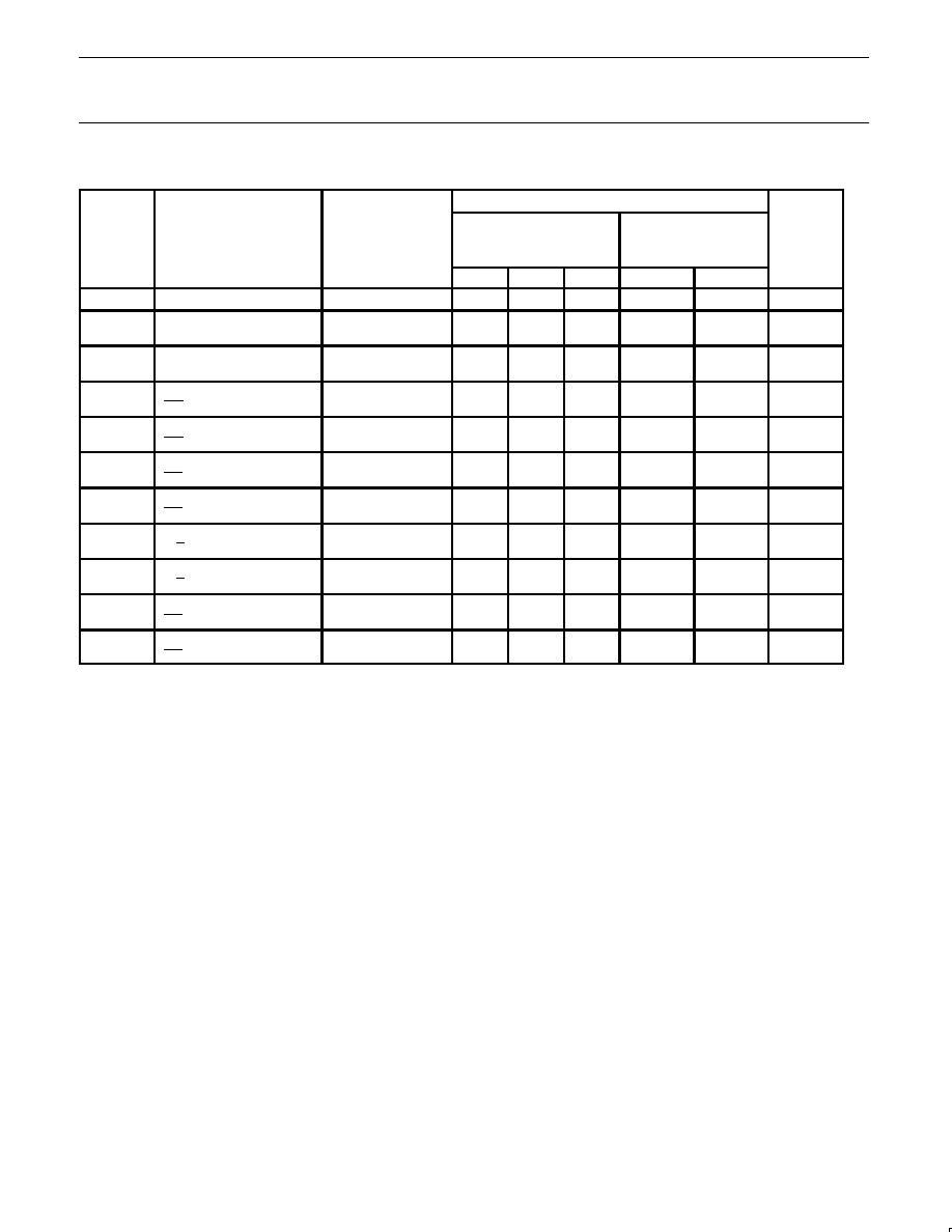
AC ELECTRICAL CHARACTERISTICS
SYMBOL
PARAMETER
TEST CONDITIONS
LIMITS
UNIT
SYMBOL
PARAMETER
TEST CONDITIONS
T
amb
= +25
∞
C
T
amb
= 0
∞
C to +70
∞
C
UNIT
SYMBOL
PARAMETER
TEST CONDITIONS
V
CC
= +5.0V
V
CC
= +5.0V
±
10%
UNIT
C
L
= 50pF, R
L
= 500
C
L
= 50pF, R
L
= 500
MIN
TYP
MAX
MIN
MAX
f
MAX
Maximum clock frequency
Waveform 1
110
125
90
MHz
t
PLH
t
PHL
Propagation delay
CP to I/On
Waveform 1
4.0
4.5
6.0
7.0
9.0
9.5
4.0
4.5
10.0
10.0
ns
ns
t
PLH
t
PHL
Propagation delay
CP to Q7
Waveform 1
4.5
5.0
6.5
6.5
9.0
9.0
4.5
5.0
10.0
9.0
ns
ns
t
PHL
Propagation delay
MR to I/On
Waveform 2
5.0
6.5
9.5
4.5
10.0
ns
t
PHL
Propagation delay
MR to Q7
Waveform 2
5.0
6.5
9.5
4.5
10.0
ns
t
PZH
t
PZL
Output Enable time
OE to I/On
Waveform 4
Waveform 5
3.0
5.5
5.0
7.5
8.0
10.5
3.0
5.0
9.0
11.0
ns
ns
t
PHZ
t
PLZ
Output Disable time
OE to I/On
Waveform 4
Waveform 5
2.0
1.0
4.0
2.5
6.5
5.5
2.0
1.0
7.5
6.0
ns
ns
t
PZH
t
PZL
Output Disable time
S/P to I/On
Waveform 4
Waveform 5
4.0
6.0
6.0
8.0
9.0
11.0
3.5
5.5
10.0
11.5
ns
ns
t
PHZ
t
PLZ
Output Disable time
S/P to I/On
Waveform 4
Waveform 5
4.0
2.0
6.0
4.0
9.0
7.0
3.5
2.0
10.5
7.5
ns
ns
t
PZH
t
PZL
Output Disable time
RE to I/On
Waveform 4
Waveform 5
8.0
9.0
9.5
11.0
12.5
14.0
7.0
8.0
14.0
16.0
ns
ns
t
PHZ
t
PLZ
Output Disable time
RE to I/On
Waveform 4
Waveform 5
6.5
4.5
8.5
6.5
11.5
9.5
5.5
4.0
13.0
10.5
ns
ns
Philips Semiconductors
Product specification
74F322
8-bit serial/parallel register with sign extend (3-State)
1988 Apr 22
7
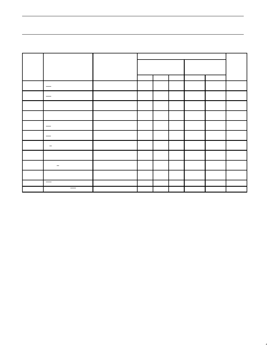
AC SETUP REQUIREMENTS
SYMBOL
PARAMETER
TEST CONDITIONS
LIMITS
UNIT
SYMBOL
PARAMETER
TEST CONDITIONS
T
amb
= +25
∞
C
T
amb
= 0
∞
C to +70
∞
C
UNIT
SYMBOL
PARAMETER
TEST CONDITIONS
V
CC
= +5.0V
V
CC
= +5.0V
±
10%
UNIT
C
L
= 50pF, R
L
= 500
C
L
= 50pF, R
L
= 500
MIN
TYP
MAX
MIN
MAX
t
s
(H)
t
s
(L)
Setup time, High or Low
RE to CP
Waveform 3
8.0
12.5
9.5
14.0
ns
ns
t
h
(H)
t
h
(L)
Hold time, High or Low
RE to CP
Waveform 3
0
0
0
0
ns
ns
t
s
(H)
t
s
(L)
Setup time, High or Low
D0, D1 or I/On to CP
Waveform 3
4.0
4.5
6.0
5.0
ns
ns
t
h
(H)
t
h
(L)
Hold time, High or Low
D0, D1 or I/On to CP
Waveform 3
0
0
0
0
ns
ns
t
s
(H)
t
s
(L)
Setup time, High or Low
SE to CP
Waveform 3
5.5
5.0
7.0
5.5
ns
ns
t
h
(H)
t
h
(L)
Hold time, High or Low
SE to CP
Waveform 3
0
0
0
0
ns
ns
t
s
(H)
t
s
(L)
Setup time, High or Low
S/P to CP
Waveform 3
10.5
9.5
11.0
10.5
ns
ns
t
s
(H)
t
s
(L)
Setup time, High or Low
S to CP
Waveform 3
4.0
8.5
4.5
9.5
ns
ns
t
h
(H)
t
h
(L)
Hold time, High or Low
S or S/P to CP
Waveform 3
0
0
0
0
ns
ns
t
w
(H)
t
w
(L)
CP Pulse width, High or Low
Waveform 3
5.0
5.0
5.0
5.0
ns
t
w
(L)
MR Pulse width, Low
Waveform 3
5.0
5.0
ns
t
REC
Recovery time, MR to CP
Waveform 2
4.0
4.5
ns
Philips Semiconductors
Product specification
74F322
8-bit serial/parallel register with sign extend (3-State)
1988 Apr 22
8
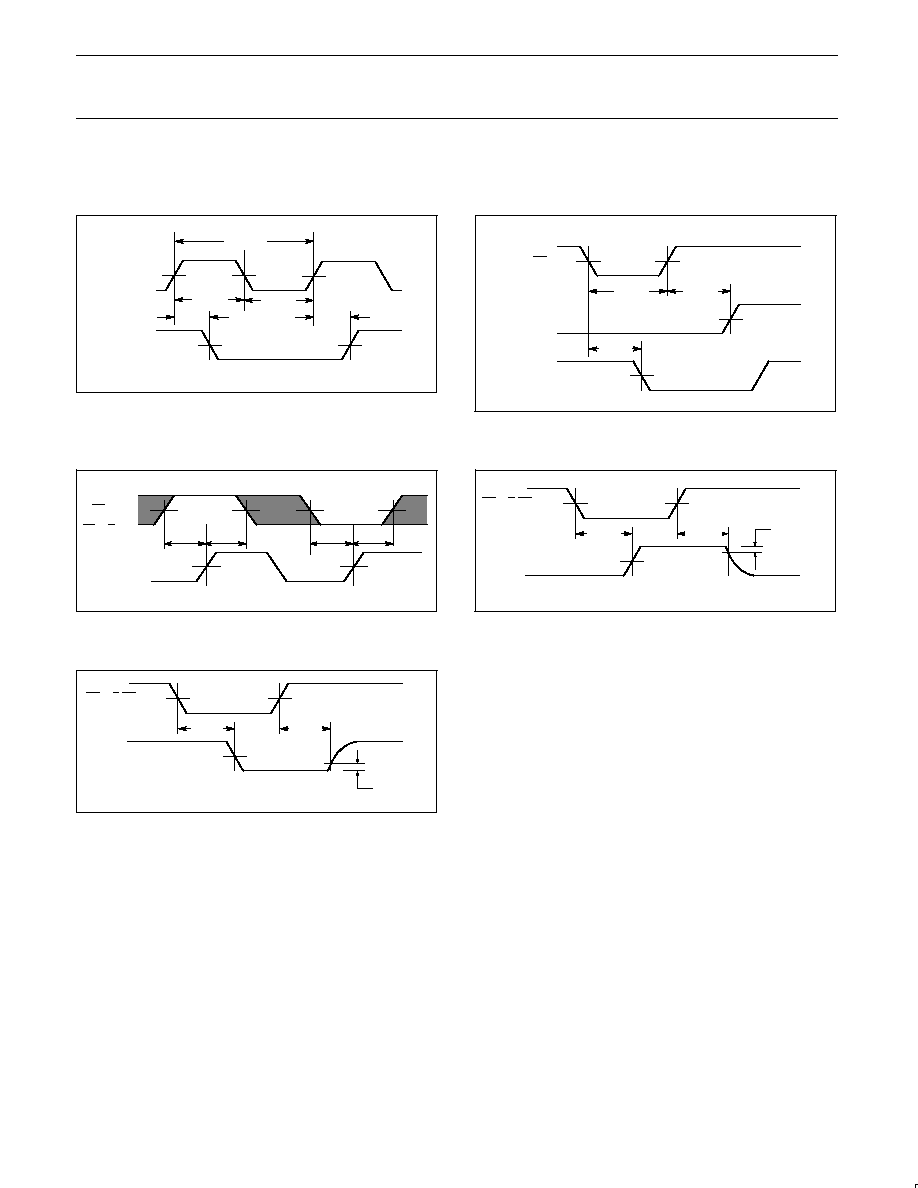
AC WAVEFORMS
For all waveforms, V
M
= 1.5V
The shaded areas indicate when the input is permitted to change for predictable output performance.
VM
tPLH
tPHL
VM
VM
VM
1/fMAX
tW(L)
CP
Q7, I/On
tW(H)
SF00878
Waveform 1. Propagation Delay, Clock Input to Output,
Clock Pulse Width, and Maximum Clock Frequency
VM
VM
VM
tPHL
tW(L)
tREC
VM
Q7, I/On
CP
MR
SF00879
Waveform 2. Master Reset Pulse Width, Master Reset to Output
Delay, and Master Reset to Clock Recovery Time
VM
VM
VM
VM
ts(H)
th(H)
th(L)
ts(L)
VM
VM
RE, D0,
D1, I/On,
SE, S/P, S
CP
SF00880
Waveform 3. Data Setup and Hold Times
VM
VM
VM
tPHZ
tPZH
RE, S/P, OE
I/On
VOH -0.3V
0V
SF00881
Waveform 4. 3-State Output Enable Time to High Level
and Output Disable Time from High Level
VM
VM
VM
tPLZ
tPZL
I/On
VOL +0.3V
SF00882
RE, S/P, OE
Waveform 5. 3-State Output Enable Time to Low Level and
Output Disable Time from Low Level
Philips Semiconductors
Product specification
74F322
8-bit serial/parallel register with sign extend (3-State)
1988 Apr 22
9
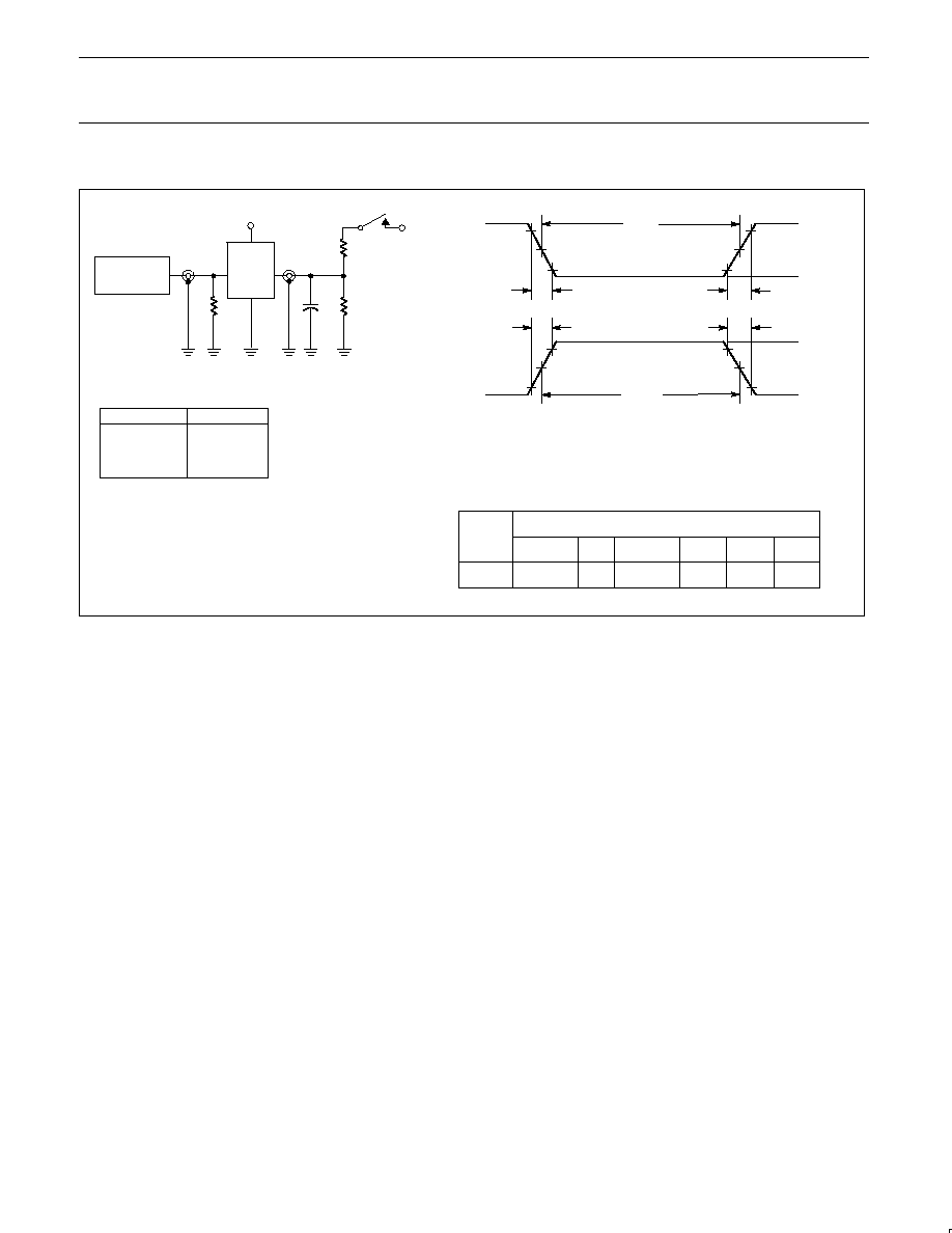
TEST CIRCUIT AND WAVEFORM
tw
90%
VM
10%
90%
VM
10%
90%
VM
10%
90%
VM
10%
NEGATIVE
PULSE
POSITIVE
PULSE
tw
AMP (V)
0V
0V
tTHL (tf
)
INPUT PULSE REQUIREMENTS
rep. rate
t
w
t
TLH
t
THL
1MHz
500ns
2.5ns
2.5ns
Input Pulse Definition
VCC
family
74F
D.U.T.
PULSE
GENERATOR
RL
CL
RT
VIN
VOUT
Test Circuit for 3-State Outputs
DEFINITIONS:
R
L
= Load resistor;
see AC electrical characteristics for value.
C
L
= Load capacitance includes jig and probe capacitance;
see AC electrical characteristics for value.
R
T
= Termination resistance should be equal to Z
OUT
of
pulse generators.
tTHL (tf
)
tTLH (tr
)
tTLH (tr
)
AMP (V)
amplitude
3.0V
1.5V
V
M
RL
7.0V
SF00777
TEST
SWITCH
t
PLZ
closed
t
PZL
closed
All other
open
SWITCH POSITION