 | –≠–ª–µ–∫—Ç—Ä–æ–Ω–Ω—ã–π –∫–æ–º–ø–æ–Ω–µ–Ω—Ç: N74F382N | –°–∫–∞—á–∞—Ç—å:  PDF PDF  ZIP ZIP |
Document Outline
- FEATURES
- DESCRIPTION
- PIN CONFIGURATION
- ORDERING INFORMATION
- INPUT AND OUTPUT LOADING AND FAN OUT TABLE
- LOGIC SYMBOL
- IEC/IEEE SYMBOL
- LOGIC DIAGRAM
- FUNCTION TABLE
- FUNCTION SELECT TABLE
- APPLICATION
- ABSOLUTE MAXIMUM RATINGS
- RECOMMENDED OPERATING CONDITIONS
- DC ELECTRICAL CHARACTERISTICS
- AC ELECTRICAL CHARACTERISTICS
- AC WAVEFORMS
- TEST CIRCUIT AND WAVEFORM
- PACKAGE OUTLINES
- Data sheet status
- Definitions
- Disclaimers

Philips
Semiconductors
74F382
Arithmetic Logic Unit
Product specification
IC15 Data Handbook
1990 Jul 12
INTEGRATED CIRCUITS
Philips Semiconductors
Product specification
74F382
Arithmetic logic unit
2
1990 Jul 12
853≠0419 99966
FEATURES
∑
Performs six arithmetic and logic functions
∑
Selectable Low (clear) and High (preset) functions
∑
Low-input loading minimizes drive requirements
∑
Carry output for ripple expansion
∑
Overflow output for Two's Complement arithmetic
DESCRIPTION
The 74F382 performs three arithmetic and three logic operations on
two 4-bit words, A and B. Two additional Select (S0≠S2) input codes
force the Function outputs Low or High. An overflow output is
provided for convenience in Two's Complement arithmetic.
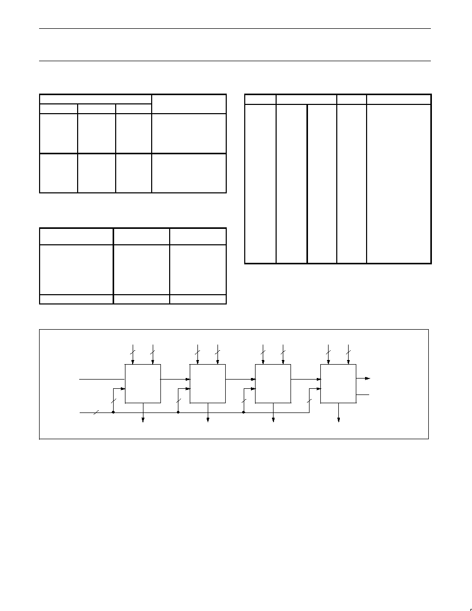
A carry output is provided for ripple expansion. For high-speed
expansion using a carry look-ahead generator, refer to the 74F381
data sheet.
Signals applied to the Select inputs, S0≠S2, determine the mode of
operation, as indicated in the Function Select Table. An extensive
listing of input and output levels is shown in the Function Table. The
circuit performs the arithmetic functions for either active-HIgh or
active-Low operands, with output levels in the same convention. In
the subtract operating modes, it is necessary to force a carry (High
for active-HIgh operands, Low for active-Low operands) into the Cn
input of the least significant package. Ripple expansion is illustrated
in Figure 1. The overflow output OVR is the Exclusive-OR of Cn+3
and Cn+4; a High signal on OVR indicates overflow in Two's
complement operation (See Table 2 for Two's complement
arithmetic). Typical delays for Figure 1 are given in Table 1. When
the 74F382 is cascaded to handle word lengths longer than 4 bits,
only the most significant overflow (OVR) output is used.
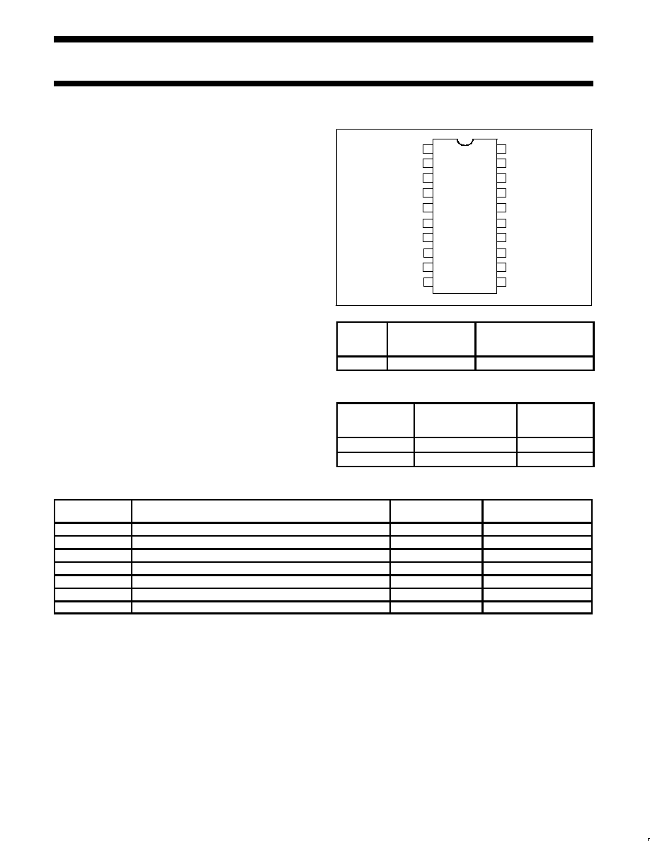
PIN CONFIGURATION
20
19
18
17
16
15
14
7
6
5
4
3
2
1
13
8
VCC
A1
B1
A0
B0
S0
S1
S2
F0
F1
GND
A2
B2
A3
B3
Cn
Cn+4
OVR
F3
F2
SF00935
12
9
11
10
TYPE
TYPICAL
PROPAGATION
DELAY
TYPICAL SUPPLY
CURRENT (TOTAL)
74F382
7.0ns
54mA
ORDERING INFORMATION
DESCRIPTION
COMMERCIAL RANGE
V
CC
= 5V
±
10%,
T
amb
= 0
∞
C to +70
∞
C
PKG DWG #
20-pin plastic DIP
N74F382N
SOT146-1
20-pin plastic SO
N74F382D
SOT163-1
INPUT AND OUTPUT LOADING AND FAN OUT TABLE
PINS
DESCRIPTION
74F (U.L.)
HIGH/LOW
LOAD VALUE
HIGH/LOW
A0 ≠ A3
A operand inputs
1.0/4.0
20
µ
A/2.4mA
B0 ≠ B3
B operand inputs
1.0/4.0
20
µ
A/2.4mA
S0 ≠ S2
Function select inputs
1.0/1.0
20
µ
A/0.6mA
Cn
Carry input
1.0/5.0
20
µ
A/3.0mA
Cn+4
Carry output
50/33
1.0mA/20mA
OVR
Overflow output
50/33
1.0mA/20mA
F0≠F3
Outputs
50/33
1.0mA/20mA
NOTE:
One (1.0) FAST unit load is defined as 20
µ
A in the High state and 0.6mA in the Low state.
Philips Semiconductors
Product specification
74F382
Arithmetic logic unit
1990 Jul 12
3
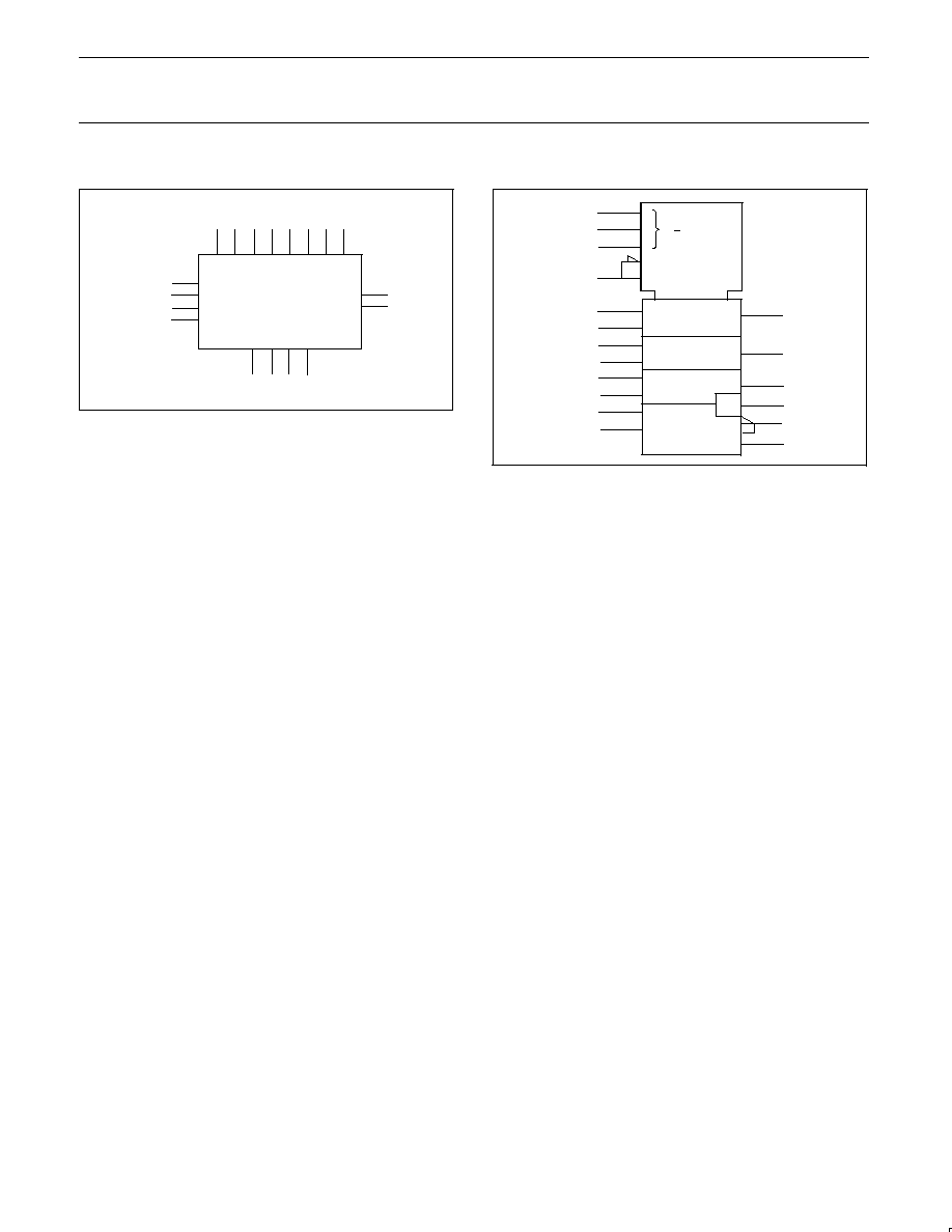
LOGIC SYMBOL
F0 F1 F2 F3
VCC = Pin 20
GND = Pin 10
A0 B0 A1 B1 A2 B2 A3 B3
3
4
1
2
19 18 17 16
Cn
S0
S1
S2
15
5
6
7
8
9
11 12
SF00936
OVR
Cn+4
13
14
IEC/IEEE SYMBOL
8
9
(1/2) Bl
15
P
SF00937
3
4
1
2
19
18
17
16
Q
P
Q
P
Q
P
Q
[1]
[2]
[4]
[8]
0
2
3 Cl
M
0
7
5
6
7
ALU
=1
BO/CO
BO/CO
(1/2)BO
3CO
11
13
14
12
Philips Semiconductors
Product specification
74F382
Arithmetic logic unit
1990 Jul 12
4
LOGIC DIAGRAM
VCC = Pin 20
GND = Pin 10
3
4
1
2
19
18
17
16
5
6
7
15
Cn
A0
B0
A1
B1
A2
B2
A3
B3
S0
S1
S2
8
9
11
12
14
13
F0
F1
F2
F3
SF00938
OVR
Cn+4

Philips Semiconductors
Product specification
74F382
Arithmetic logic unit
1990 Jul 12
5
FUNCTION TABLE
INPUTS
OUTPUTS
OPERANDS
OPERATING
S0
S1
S2
Cn
An
Bn
F0
F1
F2
F3
OVR
Cn+4
OPERANDS
MODE
L
L
L
L
X
X
L
L
L
L
H
H
Clear
L
L
L
H
X
X
L
L
L
L
H
H
Clear
H
L
L
L
L
L
H
H
H
H
L
L
H
L
L
L
L
H
L
H
H
H
L
H
Active Low
H
L
L
L
H
L
L
L
L
L
L
L
Active-Low
H
L
L
L
H
H
H
H
H
H
L
L
B minus A
H
L
L
H
L
L
L
L
L
L
L
H
B minus A
H
L
L
H
L
H
H
H
H
H
L
H
Active High
H
L
L
H
H
L
H
L
L
L
L
L
Active-High
H
L
L
H
H
H
L
L
L
L
L
H
L
H
L
L
L
L
H
H
H
H
L
L
L
H
L
L
L
H
L
L
L
L
L
L
Active Low
L
H
L
L
H
L
L
H
H
H
L
H
Active-Low
L
H
L
L
H
H
H
H
H
H
L
L
A minus B
L
H
L
H
L
L
L
L
L
L
L
H
A minus B
L
H
L
H
L
H
H
L
L
L
L
L
Active High
L
H
L
H
H
L
H
H
H
H
L
H
Active-High
L
H
L
H
H
H
L
L
L
L
L
H
H
H
L
L
L
L
L
L
L
L
L
L
H
H
L
L
L
H
H
H
H
H
L
L
H
H
L
L
H
L
H
H
H
H
L
L
H
H
L
L
H
H
L
H
H
H
L
H
A Plus B
H
H
L
H
L
L
H
L
L
L
L
L
A Plus B
H
H
L
H
L
H
L
L
L
L
L
H
H
H
L
H
H
L
L
L
L
L
L
H
H
H
L
H
H
H
H
H
H
H
L
H
L
L
H
X
L
L
L
L
L
L
L
L
L
L
H
X
L
H
H
H
H
H
L
L
L
L
H
L
H
L
H
H
H
H
L
L
A
B
L
L
H
X
H
H
L
L
L
L
H
H
L
L
H
H
H
L
H
H
H
H
H
H
H
L
H
X
L
L
L
L
L
L
L
L
H
L
H
X
L
H
H
H
H
H
L
L
H
L
H
X
H
L
H
H
H
H
L
L
A + B
H
L
H
L
H
H
H
H
H
H
L
L
H
L
H
H
H
H
H
H
H
H
H
H
L
H
H
X
L
L
L
L
L
L
H
H
L
H
H
X
L
H
L
L
L
L
L
L
L
H
H
X
H
L
L
L
L
L
H
H
AB
L
H
H
L
H
H
H
H
H
H
L
L
L
H
H
H
H
H
H
H
H
H
H
H
H
H
H
X
L
L
H
H
H
H
L
L
H
H
H
X
L
H
H
H
H
H
L
L
H
H
H
X
H
L
H
H
H
H
L
L
Preset
H
H
H
L
H
H
H
H
H
H
L
L
H
H
H
H
H
H
H
H
H
H
H
H
H = High voltage level
L
= Low voltage level
X = Don't care
Philips Semiconductors
Product specification
74F382
Arithmetic logic unit
1990 Jul 12
6
FUNCTION SELECT TABLE
SELECT
OPERATING
S0
S1
S2
MODE
L
L
L
Clear
H
L
L
B minus A
L
H
L
A minus B
H
H
L
A Plus B
L
L
H
A
B
H
L
H
A + B
L
H
H
AB
H
H
H
Preset
H = High voltage level
L
= Low voltage level
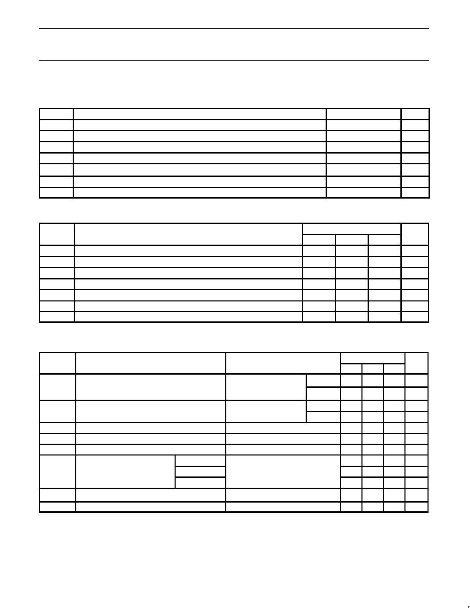
Table 1. 16-Bit Delay Tabulation
PATH SEGMENT
TOWARD
F
OUTPUT
Cn+4, OVR
Ai or Bi to Cn+4
6.5ns
6.5ns
Cn to Cn+4
6.3ns
6.3ns
Cn to Cn+4
6.3ns
6.3ns
Cn to F
8.1ns
≠
Cn to Cn+4, OVR
≠
8.0ns
Total Delay
27.2ns
27.1ns
Table 2. Two's Complement Arithmetic
MSB
LSB
Numerical Values
L
L
L
L
0
L
L
L
H
1
L
L
H
L
2
L
L
H
H
3
L
H
L
L
4
L
H
L
H
5
L
H
H
L
6
L
H
H
H
7
H
L
L
L
≠8
H
L
L
H
≠7
H
L
H
L
≠6
H
L
H
H
≠5
H
H
L
L
≠4
H
H
L
H
≠3
H
H
H
L
≠2
H
H
H
H
≠1
H = High voltage level
L
= Low voltage level
APPLICATION
A
B
Cn
SF00939
C
IN
S
F
74F382
F0≠F3
4
4
3
3
A0≠A3
B0≠B3
A
B
Cn
S
F
74F382
F4≠F7
4
4
3
A4≠A7
B4≠B7
A
B
Cn
S
F
74F382
F8≠F11
4
4
3
A8≠A11
B8≠B11
A
B
Cn
S
F
74F382
F12≠F15
4
4
3
A12≠A15
B12≠B15
Cn+4
OVR
OVERFLOW
C
OUT
SELECT
Cn+4
Cn+4
Cn+4
Figure 1. 16-bit Look-ahead Carry ALU Expansion
Philips Semiconductors
Product specification
74F382
Arithmetic logic unit
1990 Jul 12
7
ABSOLUTE MAXIMUM RATINGS
(Operation beyond the limit set forth in this table may impair the useful life of the device. Unless otherwise noted these limits are over the
operating free-air temperature range.)
SYMBOL
PARAMETER
RATING
UNIT
V
CC
Supply voltage
≠0.5 to +7.0
V
V
IN
Input voltage
≠0.5 to +7.0
V
I
IN
Input current
≠30 to +1
mA
V
OUT
Voltage applied to output in High output state
≠0.5 to +V
CC
V
I
OUT
Current applied to output in Low output state
40
mA
T
amb
Operating free-air temperature range
0 to +70
∞
C
T
stg
Storage temperature range
≠65 to +150
∞
C
RECOMMENDED OPERATING CONDITIONS
SYMBOL
PARMETER
LIMITS
UNIT
SYMBOL
SYMBOL
PARMETER
MIN
NOM
MAX
UNIT
V
CC
Supply voltage
4.5
5.0
5.5
V
V
IH
High-level input voltage
2.0
V
V
IL
Low-level input voltage
0.8
V
I
IK
Input clamp current
≠18
mA
I
OH
High-level output current
≠1
mA
I
OL
Low-level output current
20
mA
T
amb
Operating free-air temperature range
0
70
∞
C
DC ELECTRICAL CHARACTERISTICS
(Over recommended operating free-air temperature range unless otherwise noted.)
SYMBOL
PARAMETER
TEST
LIMITS
UNIT
SYMBOL
PARAMETER
CONDITIONS
1
MIN
TYP
2
MAX
V
High level output voltage
V
CC
= MIN, V
IL
= MAX,
±
10%V
CC
2.5
V
V
OH
High-level output voltage
V
IH
= MIN, I
OH
= MAX
±
5%V
CC
2.7
3.4
V
V
O
Low level output voltage
V
CC
= MIN, V
IL
= MAX,
±
10%V
CC
0.30
0.50
V
V
OL
Low-level output voltage
V
IH
= MIN, I
OL
= MAX
±
5%V
CC
0.30
0.50
V
V
IK
Input clamp voltage
V
CC
= MIN, I
I
= I
IK
≠0.73
≠1.2
V
I
I
Input current at maximum input voltage
V
CC
= MAX, V
I
= 7.0V
100
µ
A
I
IH
High-level input current
V
CC
= MAX, V
I
= 2.7V
20
µ
A
Cn
≠3.0
mA
I
IL
Low-level input current
A0≠A3, B0≠B3
V
CC
= MAX, V
I
= 0.5V
≠2.4
mA
S0, S1, S2
≠0.6
mA
I
OS
Short-circuit output current
3
V
CC
= MAX
≠60
≠150
mA
I
CC
Supply current (total)
V
CC
= MAX
54
81
mA
NOTES:
1. For conditions shown as MIN or MAX, use the appropriate value specified under recommended operating conditions for the applicable type.
2. All typical values are at V
CC
= 5V, T
amb
= 25
∞
C.
3. Not more than one output should be shorted at a time. For testing I
OS
, the use of high-speed test apparatus and/or sample-and-hold
techniques are preferable in order to minimize internal heating and more accurately reflect operational values. Otherwise, prolonged shorting
of a High output may raise the chip temperature well above normal and thereby cause invalid readings in other parameter tests. In any
sequence of parameter tests, I
OS
tests should be performed last.
Philips Semiconductors
Product specification
74F382
Arithmetic logic unit
1990 Jul 12
8
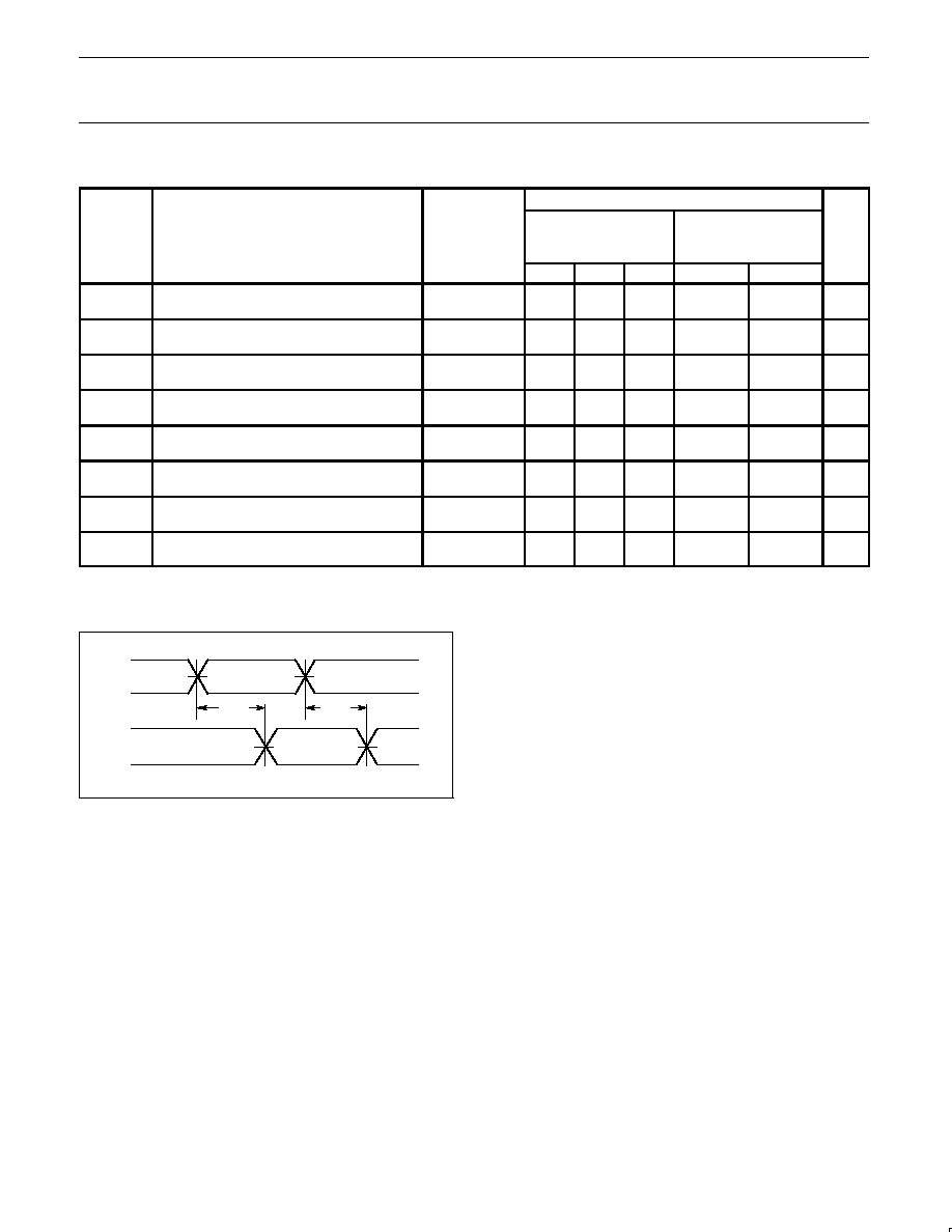
AC ELECTRICAL CHARACTERISTICS
LIMITS
T
amb
= +25
∞
C
T
amb
= 0
∞
C to +70
∞
C
SYMBOL
PARAMETER
TEST
V
CC
= +5.0V
V
CC
= +5.0V
±
10%
UNIT
CONDITION
C
L
= 50pF, R
L
= 500
C
L
= 50pF, R
L
= 500
MIN
TYP
MAX
MIN
MAX
t
PLH
t
PHL
Propagation delay
Cn to Fn
Waveform 1
3.0
2.5
7.0
4.5
12.0
6.5
2.5
2.5
13.5
7.5
ns
t
PLH
t
PHL
Propagation delay
An or Bn to Fn
Waveform 1
3.5
3.0
8.0
6.0
13.5
10.0
3.5
2.5
17.0
11.0
ns
t
PLH
t
PHL
Propagation delay
Si to Fi
Waveform 1
5.5
5.5
9.0
7.5
15.0
10.5
5.5
5.5
16.0
12.0
ns
t
PLH
t
PHL
Propagation delay
Ai to Bi to Cn+4
Waveform 1
3.5
3.5
7.0
6.5
10.5
9.5
3.5
3.5
11.5
10.5
ns
t
PLH
t
PHL
Propagation delay
Si to OVR or Cn+4
Waveform 1
7.0
5.0
10.5
8.0
14.5
11.0
6.5
5.0
17.0
12.0
ns
t
PLH
t
PHL
Propagation delay
Cn to Cn+4
Waveform 1
3.0
3.5
4.5
5.0
6.0
6.5
2.5
3.5
6.5
7.0
ns
t
PLH
t
PHL
Propagation delay
Cn to OVR
Waveform 1
4.5
3.0
9.0
5.0
13.5
6.5
4.0
3.0
15.0
7.0
ns
t
PLH
t
PHL
Propagation delay
Ai or Bi to OVR
Waveform 1
6.0
3.5
9.0
6.5
12.5
9.0
5.5
3.5
16.5
10.0
ns
AC WAVEFORMS
For all waveforms, V
M
= 1.5V.
V
M
V
M
V
M
V
M
V
OUT
V
IN
t
PHL
t
PLH
SF00940
Waveform 1. Propagation Delay for Non-Inverting
or Inverting paths
Philips Semiconductors
Product specification
74F382
Arithmetic logic unit
1990 Jul 12
9
TEST CIRCUIT AND WAVEFORM
tw
90%
VM
10%
90%
VM
10%
90%
VM
10%
90%
VM
10%
NEGATIVE
PULSE
POSITIVE
PULSE
tw
AMP (V)
0V
0V
tTHL (tf
)
INPUT PULSE REQUIREMENTS
rep. rate
t
w
t
TLH
t
THL
1MHz
500ns
2.5ns
2.5ns
Input Pulse Definition
VCC
family
74F
D.U.T.
PULSE
GENERATOR
RL
CL
RT
VIN
VOUT
Test Circuit for Totem-Pole Outputs
DEFINITIONS:
R
L
= Load resistor;
see AC ELECTRICAL CHARACTERISTICS for value.
C
L
= Load capacitance includes jig and probe capacitance;
see AC ELECTRICAL CHARACTERISTICS for value.
R
T
= Termination resistance should be equal to Z
OUT
of
pulse generators.
tTHL (tf
)
tTLH (tr
)
tTLH (tr
)
AMP (V)
amplitude
3.0V
1.5V
V
M
SF00006
Philips Semiconductors
Product specification
74F382
Arithmetic Logic Unit
1990 Jul 12
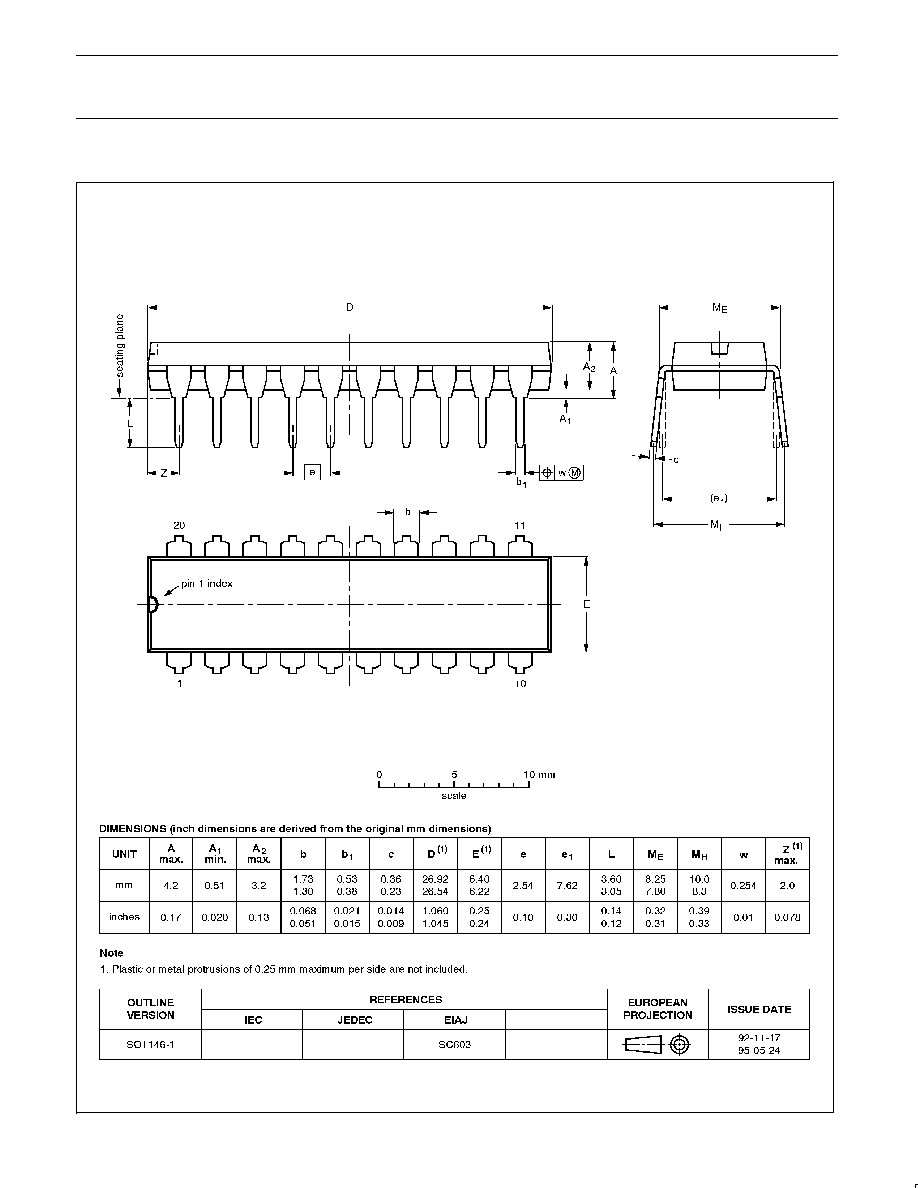
10
DIP20:
plastic dual in-line package; 20 leads (300 mil)
SOT146-1
Philips Semiconductors
Product specification
74F382
Arithmetic Logic Unit
1990 Jul 12
11
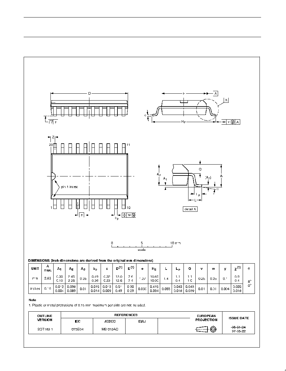
SO20:
plastic small outline package; 20 leads; body width 7.5 mm
SOT163-1
Philips Semiconductors
Product specification
74F382
Arithmetic Logic Unit
yyyy mmm dd
12
Definitions
Short-form specification -- The data in a short-form specification is extracted from a full data sheet with the same type number and title. For
detailed information see the relevant data sheet or data handbook.
Limiting values definition -- Limiting values given are in accordance with the Absolute Maximum Rating System (IEC 134). Stress above one
or more of the limiting values may cause permanent damage to the device. These are stress ratings only and operation of the device at these or
at any other conditions above those given in the Characteristics sections of the specification is not implied. Exposure to limiting values for extended
periods may affect device reliability.
Application information -- Applications that are described herein for any of these products are for illustrative purposes only. Philips
Semiconductors make no representation or warranty that such applications will be suitable for the specified use without further testing or
modification.
Disclaimers
Life support -- These products are not designed for use in life support appliances, devices or systems where malfunction of these products can
reasonably be expected to result in personal injury. Philips Semiconductors customers using or selling these products for use in such applications
do so at their own risk and agree to fully indemnify Philips Semiconductors for any damages resulting from such application.
Right to make changes -- Philips Semiconductors reserves the right to make changes, without notice, in the products, including circuits, standard
cells, and/or software, described or contained herein in order to improve design and/or performance. Philips Semiconductors assumes no
responsibility or liability for the use of any of these products, conveys no license or title under any patent, copyright, or mask work right to these
products, and makes no representations or warranties that these products are free from patent, copyright, or mask work right infringement, unless
otherwise specified.
Philips Semiconductors
811 East Arques Avenue
P.O. Box 3409
Sunnyvale, California 94088≠3409
Telephone 800-234-7381
©
Copyright Philips Electronics North America Corporation 1998
All rights reserved. Printed in U.S.A.
print code
Date of release: 10-98
Document order number:
9397-750-05124
Philips
Semiconductors
Data sheet
status
Objective
specification
Preliminary
specification
Product
specification
Product
status
Development
Qualification
Production
Definition
[1]
This data sheet contains the design target or goal specifications for product development.
Specification may change in any manner without notice.
This data sheet contains preliminary data, and supplementary data will be published at a later date.
Philips Semiconductors reserves the right to make chages at any time without notice in order to
improve design and supply the best possible product.
This data sheet contains final specifications. Philips Semiconductors reserves the right to make
changes at any time without notice in order to improve design and supply the best possible product.
Data sheet status
[1]
Please consult the most recently issued datasheet before initiating or completing a design.