 | –≠–ª–µ–∫—Ç—Ä–æ–Ω–Ω—ã–π –∫–æ–º–ø–æ–Ω–µ–Ω—Ç: N74F385N | –°–∫–∞—á–∞—Ç—å:  PDF PDF  ZIP ZIP |
Document Outline
- FEATURES
- DESCRIPTION
- PIN CONFIGURATION
- ORDERING INFORMATION
- INPUT AND OUTPUT LOADING AND FAN OUT TABLE
- LOGIC SYMBOL
- IEC/IEEE SYMBOL
- FUNCTION TABLE
- LOGIC DIAGRAM
- ABSOLUTE MAXIMUM RATINGS
- RECOMMENDED OPERATING CONDITIONS
- DC ELECTRICAL CHARACTERISTICS
- AC ELECTRICAL CHARACTERISTICS
- AC SETUP REQUIREMENTS
- AC WAVEFORMS
- TEST CIRCUIT AND WAVEFORM

Philips Semiconductors
Product specification
74F385
Quad serial adder/subtractor
1
1989 Sep 20
853≠0868 97678
FEATURES
∑
Four independent adders/subtractors
∑
Two's complement arithmetic
∑
Synchronous operation
∑
Common Clear and Clock
∑
74F385 is designed for use with serial multipliers in implementing
digital filters and butterfly networks in fast Fourier transforms
DESCRIPTION
The 74F385 contains four independent adder/subtractor elements
with common Clock and Master Reset. Each adder/subtractor
contains a sum flop-flop and a carry flip-flop for synchronous
operations. Flip-flop state changes occur on the rising edge of the
Clock Pulse (CP) input signal. The Select (S) input should be Low
for the Add (A plus B) mode and High for the Subtract (A minus B)
mode. A Low signal on the asynchronous Master Reset (MR) input
clears the sum flip-flop and resets the Carry flip-flop to zero in the
Add mode or presets it to one in the Subtract mode.
PIN CONFIGURATION
20
19
18
17
16
15
14
7
6
5
4
3
2
1
13
8
VCC
CP
F0
S0
B0
A0
A1
B1
S1
F1
GND
F3
S3
B3
A3
A2
B2
S2
F2
MR
SF00928
12
9
11
10
TYPE
TYPICAL f
MAX
TYPICAL SUPPLY
CURRENT (TOTAL)
74F385
140 MHz
55mA
ORDERING INFORMATION
DESCRIPTION
COMMERCIAL RANGE
V
CC
= 5V
±
10%, T
amb
= 0
∞
C to +70
∞
C
20-pin plastic DIP
N74F385N
20-pin plastic SO
N74F385D
INPUT AND OUTPUT LOADING AND FAN OUT TABLE
PINS
DESCRIPTION
74F (U.L.)
HIGH/LOW
LOAD VALUE
HIGH/LOW
A0 ≠ A3
A operand inputs
1.0/1.0
20
µ
A/0.6mA
B0 ≠ B3
B operand inputs
1.0/1.0
20
µ
A/0.6mA
S0 ≠ S3
Function select inputs
1.0/1.0
20
µ
A/0.6mA
CP
Clock pulse input (active rising edge)
1.0/1.0
20
µ
A/0.6mA
MR
Asynchronous Master Reset input (active Low)
1.0/1.0
20
µ
A/0.6mA
F0≠F3
Sum or difference outputs
50/33
1.0mA/20mA
NOTE:
One (1.0) FAST unit load is defined as: 20
µ
A in the High state and 0.6mA in the Low state.

Philips Semiconductors
Product specification
74F385
Quad serial adder/subtractor
1989 Sep 20
2
LOGIC SYMBOL
F0 F1 F2 F3
VCC = Pin 20
GND = Pin 10
A0 B0 A1 B1 A2 B2 A3 B3
5
4
6
7
15 14 16 17
CP
MR
S0
S1
S2
S3
1
11
3
8
13
18
2
9
12 19
SF00929
IEC/IEEE SYMBOL
9
11
19
5
P
SF00930
8
6
7
13
15
14
18
16
Q
11
1
2
17
M3
4(3CI/ 3BI)
3CO/ 3BO
S
/P≠Q
Z4
2D
R
2D
3R
3S
3
4
Z1
C2
FUNCTION TABLE
INPUTS
CARRY
FLIP-FLOP STATE
OUTPUTS
OPERATING
MODE
MR
S
A
B
Before
After
F
MODE
L
L
X
X
L
L
L
Clear
L
H
X
X
H
H
L
Clear
H
L
L
L
L
L
L
Add
H
L
L
L
H
L
H
Add
H
L
L
H
L
L
H
Add
H
L
L
H
H
H
L
Add
H
L
H
L
L
L
H
Add
H
L
H
L
H
H
L
H
L
H
H
L
H
L
H
L
H
H
H
H
H
H
H
L
L
L
L
H
Subtract
H
H
L
L
H
H
L
Subtract
H
H
L
H
L
L
L
Subtract
H
H
L
H
H
L
H
Subtract
H
H
H
L
L
H
L
Subtract
H
H
H
L
H
H
H
H
H
H
H
L
L
H
H
H
H
H
H
H
L
H = High voltage level
L
= Low voltage level
X = Don't care
= Low-to-High Clock transition
Philips Semiconductors
Product specification
74F385
Quad serial adder/subtractor
1989 Sep 20
3
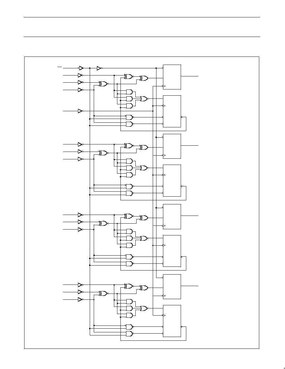
LOGIC DIAGRAM
VCC = Pin 20
GND = Pin 10
11
SF00931
5
4
3
1
MR
A0
B0
S0
CP
R
D
CP
Q
SUM
D
CP
S
R
Q
F0
2
6
7
8
A1
B1
S1
R
D
CP
Q
SUM
D
CP
S
R
Q
F1
9
15
14
13
A2
B2
S2
R
D
CP
Q
SUM
D
CP
S
R
Q
F2
12
16
17
18
A3
B3
S3
R
D
CP
Q
SUM
D
CP
S
R
Q
F3
19
CARRY
CARRY
CARRY
CARRY

Philips Semiconductors
Product specification
74F385
Quad serial adder/subtractor
1989 Sep 20
4
ABSOLUTE MAXIMUM RATINGS
(Operation beyond the limit set forth in this table may impair the useful life of the device. Unless otherwise noted these limits are over the
operating free-air temperature range.)
SYMBOL
PARAMETER
RATING
UNIT
V
CC
Supply voltage
≠0.5 to +7.0
V
V
IN
Input voltage
≠0.5 to +7.0
V
I
IN
Input current
≠30 to +5
mA
V
OUT
Voltage applied to output in High output state
≠0.5 to V
CC
V
I
OUT
Current applied to output in Low output state
40
mA
T
amb
Operating free-air temperature range
0 to +70
∞
C
T
stg
Storage temperature
≠65 to +150
∞
C
RECOMMENDED OPERATING CONDITIONS
SYMBOL
PARMETER
LIMITS
UNIT
SYMBOL
PARMETER
MIN
NOM
MAX
UNIT
V
CC
Supply voltage
4.5
5.0
5.5
V
V
IH
High-level input voltage
2.0
V
V
IL
Low-level input voltage
0.8
V
I
IK
Input clamp current
≠18
mA
I
OH
High-level output current
≠1
mA
I
OL
Low-level output current
20
mA
T
amb
Operating free-air temperature range
0
70
∞
C
DC ELECTRICAL CHARACTERISTICS
(Over recommended operating free-air temperature range unless otherwise noted.)
SYMBOL
PARAMETER
TEST
LIMITS
UNIT
SYMBOL
PARAMETER
CONDITIONS
1
MIN
TYP
2
MAX
V
OH
High-level output voltage
V
CC
= MIN, V
IL
= MAX,
±
10%V
CC
2.5
V
V
OH
High-level output voltage
V
IH
= MIN, I
OH
= MAX
±
5%V
CC
2.7
3.4
V
V
OL
Low-level output voltage
V
CC
= MIN, V
IL
= MAX,
±
10%V
CC
0.35
0.50
V
V
OL
Low-level output voltage
V
IH
= MIN, I
OL
= MAX
±
5%V
CC
0.35
0.50
V
V
IK
Input clamp voltage
V
CC
= MIN, I
I
= I
IK
≠0.73
≠1.2
V
I
I
Input current at maximum input voltage
V
CC
= MAX, V
I
= 7.0V
100
µ
A
I
IH
High-level input current
V
CC
= MAX, V
I
= 2.7V
20
µ
A
I
IL
Low-level input current
V
CC
= MAX, V
I
= 0.5V
≠20
µ
A
I
OS
Short-circuit output current
3
V
CC
= MAX
≠60
≠150
mA
I
CC
Supply current (total)
V
CC
= MAX
55
80
mA
Notes:
1. For conditions shown as MIN or MAX, use the appropriate value specified under recommended operating conditions for the applicable type.
2. All typical values are at V
CC
= 5V, T
amb
= 25
∞
C.
3. Not more than one output should be shorted at a time. For testing I
OS
, the use of high-speed test apparatus and/or sample-and-hold
techniques are preferable in order to minimize internal heating and more accurately reflect operational values. Otherwise, prolonged shorting
of a High output may raise the chip temperature well above normal and thereby cause invalid readings in other parameter tests. In any
sequence of parameter tests, I
OS
tests should be performed last.

Philips Semiconductors
Product specification
74F385
Quad serial adder/subtractor
1989 Sep 20
5
AC ELECTRICAL CHARACTERISTICS
LIMITS
T
amb
= +25
∞
C
T
amb
= 0
∞
C to +70
∞
C
SYMBOL
PARAMETER
TEST
V
CC
= +5.0V
V
CC
= +5.0V
±
10%
UNIT
CONDITION
C
L
= 50pF, R
L
= 500
C
L
= 50pF, R
L
= 500
MIN
TYP
MAX
MIN
MAX
f
MAX
Maximum clock frequency
Waveform 1
105
140
90
MHz
t
PLH
t
PHL
Propagation delay,
Cn to Fn
Waveform 1
3.0
3.5
5.0
5.5
8.0
9.0
2.5
3.5
9.0
10.0
ns
t
PLH
Propagation delay, MR to Fn
Waveform 2
4.0
6.5
9.5
4.0
10.5
ns
AC SETUP REQUIREMENTS
LIMITS
T
amb
= +25
∞
C
T
amb
= 0
∞
C to +70
∞
C
SYMBOL
PARAMETER
TEST
V
CC
= +5.0V
V
CC
= +5.0V
±
10%
UNIT
CONDITION
C
L
= 50pF, R
L
= 500
C
L
= 50pF, R
L
= 500
MIN
TYP
MAX
MIN
MAX
t
s
(H)
t
s
(L)
Setup time, High or Low
An, Bn or Sn to CP
Waveform 3
12.0
12.0
12.0
12.0
ns
t
h
(H)
t
h
(L)
Hold time, High or Low
An, Bn or Sn to CP
Waveform 3
0
0
0
0
ns
t
s
(H)
t
s
(L)
CP Pulse width
High or Low
Waveform 2
6.0
6.0
6.0
6.0
ns
t
w
(L)
MR Pulse width
Low
Waveform 2
6.0
6.0
ns
t
REC
(L)
Recovery time
MR to CP
Waveform 2
8.5
9.5
ns
AC WAVEFORMS
For all waveforms, V
M
= 1.5V.
The shaded areas indicate when the input is permitted to change for predictable output performances.
CP
VM
VM
VM
tw(H)
1/fmax
VM
VM
tPLH
tw(L)
tPHL
Fn
SF00932
Waveform 1. Propagation Delay, Clock Input to Output,
Clock Pulse Width, and Maximum Clock Frequency
VM
VM
VM
VM
Fn
MR
tPHL
tREC
SF00933
CP
tW
(L)
Waveform 2. Master Reset Pulse Width,
Master Reset to Output Delay and
Master Reset to Clock Recovery Time
VM
VM
VM
VM
VM
VM
ts(L)
th(L)
ts(H)
th(H)
An, Bn, Sn
CP
SF00934
Waveform 3. Data and Select Setup and Hold Times

Philips Semiconductors
Product specification
74F385
Quad serial adder/subtractor
1989 Sep 20
6
TEST CIRCUIT AND WAVEFORM
tw
90%
VM
10%
90%
VM
10%
90%
VM
10%
90%
VM
10%
NEGATIVE
PULSE
POSITIVE
PULSE
tw
AMP (V)
0V
0V
tTHL (tf
)
INPUT PULSE REQUIREMENTS
rep. rate
t
w
t
TLH
t
THL
1MHz
500ns
2.5ns
2.5ns
Input Pulse Definition
VCC
family
74F
D.U.T.
PULSE
GENERATOR
RL
CL
RT
VIN
VOUT
Test Circuit for Totem-Pole Outputs
DEFINITIONS:
R
L
= Load resistor;
see AC ELECTRICAL CHARACTERISTICS for value.
C
L
= Load capacitance includes jig and probe capacitance;
see AC ELECTRICAL CHARACTERISTICS for value.
R
T
= Termination resistance should be equal to Z
OUT
of
pulse generators.
tTHL (tf
)
tTLH (tr
)
tTLH (tr
)
AMP (V)
amplitude
3.0V
1.5V
V
M
SF00006