 | –≠–ª–µ–∫—Ç—Ä–æ–Ω–Ω—ã–π –∫–æ–º–ø–æ–Ω–µ–Ω—Ç: N74F395N | –°–∫–∞—á–∞—Ç—å:  PDF PDF  ZIP ZIP |
Document Outline
- FEATURES
- DESCRIPTION
- PIN CONFIGURATION
- ORDERING INFORMATION
- INPUT AND OUTPUT LOADING AND FAN-OUT TABLE
- LOGIC SYMBOL
- IEC/IEEE SYMBOL (IEEE/IEC)
- LOGIC DIAGRAM
- MODE SELECTÖFUNCTION TABLE
- ABSOLUTE MAXIMUM RATINGS
- RECOMMENDED OPERATING CONDITIONS
- DC ELECTRICAL CHARACTERISTICS
- AC ELECTRICAL CHARACTERISTICS
- AC SETUP REQUIREMENTS
- AC WAVEFORMS
- TEST CIRCUIT AND WAVEFORMS
Philips Semiconductors
Product specification
74F395
4-bit cascadable shift register (3-State)
1
1990 Oct 23
853≠0370 00780
FEATURES
∑
4-bit parallel load shift register
∑
Independent 3-State buffer outputs, Q0≠Q3
∑
Separate Qs output for serial expansion
∑
Asynchronous Master Reset
DESCRIPTION
The 74F395 is a 4-bit Shift Register with serial and parallel
synchronous operating modes and 3-State buffer outputs. The
shifting and loading operations are controlled by the state of the
Parallel Enable (PE) input. When PE is High, data is loaded from the
Parallel Data inputs (D0≠D3) into the register synchronous with the
High-to-Low transition of the Clock input (CP). When PE is Low, the
data at the Serial Data input (Ds) is loaded into the Q0 flip-flop, and
the data in the register is shifted one bit to the right in the direction
(Q0
!
Q1
!
Q2
!
Q3) synchronous with the negative clock transition.
The PE and Data inputs are fully edge-triggered and must be stable
one setup prior to the High-to-Low transition of the clock.
The Master Reset (MR) is an asynchronous active-Low input. When
Low, the MR overrides the clock and all other inputs and clears the
register.
The 3-state output buffers are designed to drive heavily loaded
3-State buses, or large capacitive loads.
The active-Low Output Enable (OE) controls all four 3-State buffers
independent of the register operation. The data in the register
appears at the outputs when OE is Low. The outputs are in High
impedance "OFF" state, which means they will neither drive nor load
the bus when OE is High. The output from the last stage is brought
out separately. This output (Qs) is tied to the Serial Data input (Ds)
of the next register for serial expansion applications. The Qs output
is not affected by the 3-State buffer operation.
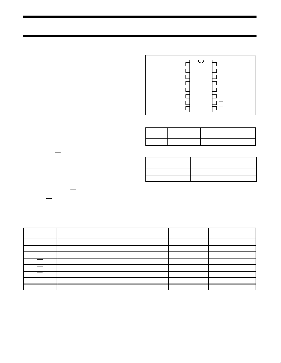
PIN CONFIGURATION
16
15
14
13
12
11
10
7
6
5
4
3
2
1
PE
V
CC
Q3
Qs
CP
Q2
Q0
Q1
MR
Ds
D3
D0
D1
D2
SF00940
9
8
GND
OE
TYPE
TYPICAL f
MAX
TYPICAL SUPPLY CURRENT
(TOTAL)
74F395
120MHz
32mA
ORDERING INFORMATION
DESCRIPTION
COMMERCIAL RANGE
V
CC
= 5V
±
10%, T
amb
= 0
∞
C to +70
∞
C
16-pin plastic DIP
N74F395N
16-pin plastic SO
N74F395D
INPUT AND OUTPUT LOADING AND FAN-OUT TABLE
PINS
DESCRIPTION
74F (U.L.)
HIGH/LOW
LOAD VALUE
HIGH/LOW
D0 ≠ D3
Data inputs
1.0/1.0
20
µ
A/0.6mA
Ds
Serial data input
1.0/1.0
20
µ
A/0.6mA
PE
Parallel Enable input
1.0/1.0
20
µ
A/0.6mA
MR
Master Reset input (active Low)
1.0/1.0
20
µ
A/0.6mA
OE
Output Enable input (active Low)
1.0/1.0
20
µ
A/0.6mA
CP
Clock Pulse input (active falling edge)
1.0/1.0
20
µ
A/0.6mA
Qs
Serial expansion output
50/33
1.0mA/20mA
Q0≠Q3
Data outputs (3-State)
150/40
3.0mA/24mA
NOTE:
One (1.0) FAST unit load is defined as: 20
µ
A in the High state and 0.6mA in the Low state.

Philips Semiconductors
Product specification
74F395
4-bit cascadable shift register (3-State)
1990 Oct 23
2
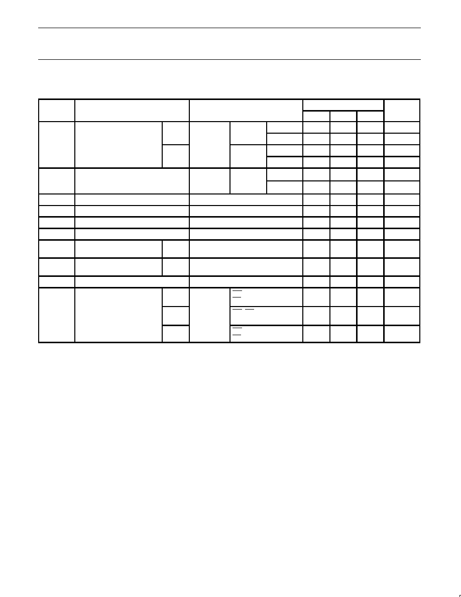
LOGIC SYMBOL
10
7
PE
CP
15
14
13
12
Q0
Q1
Q2
Q3
1
9
OE
MR
SF00941
VCC = Pin 16
GND = Pin 8
3
4
5
6
D0
D1
D2
D3
2
Ds
11
Qs
IEC/IEEE SYMBOL (IEEE/IEC)
10
2,3D
SF00942
2
4
5
6
1,3D
R
M1[LOAD]
C3/2
!
1
9
7
SRG4
13
12
11
EN4
M2[SHIFT]
4
4
3
1,3D
15
14
LOGIC DIAGRAM
VCC = Pin 16
GND = Pin 8
SF00943
R
Q
CLR
CP
Q
S
R
Q
CLR
CP
Q
S
R
Q
CLR
CP
Q
S
R
Q
CLR
CP
Q
S
15
14
13
12
11
Q0
Q1
Q2
Q3
Qs
OE
CP
MR
PE
Ds
D0
D1
D2
D3
9
10
1
7
2
3
4
5
6

Philips Semiconductors
Product specification
74F395
4-bit cascadable shift register (3-State)
1990 Oct 23
3
MODE SELECT≠FUNCTION TABLE
INPUTS
OUTPUTS
REGISTER
OPERATING
MODES
MR
CP
PE
Ds
Dn
Q0
Q1
Q2
Q3
OPERATING
MODES
L
X
X
X
X
L
L
L
L
Reset (clear)
H
#
l
l
X
L
q0
q1
q2
Shift right
H
#
l
h
X
H
q0
q1
q2
Shift right
H
#
h
X
l
L
L
L
L
Parallel load
H
#
h
X
h
H
H
H
H
Parallel load
INPUTS
OUTPUTS
3-STATE BUFFER
OPERATING
MODES
OE
Qn (Register)
Q0, Q1, Q2, Q3
Qs
OPERATING
MODES
L
L
L
L
Read
L
H
H
H
Read
H
L
Z
L
Disable buffers
H
H
Z
H
Disable buffers
H = High voltage level
h
= High voltage level one set-up time prior to the High-to-Low
clock transition
L
= Low voltage level
l
= Low voltage level one set-up time prior to the High-to-Low
clock transition
qn = Lower case letters indicate the state of the referenced input
(or output) one set-up time prior to the High-to-Low clock
transition
X = Don't care
Z = High impedance "OFF" state
#
= High-to-Low clock transition
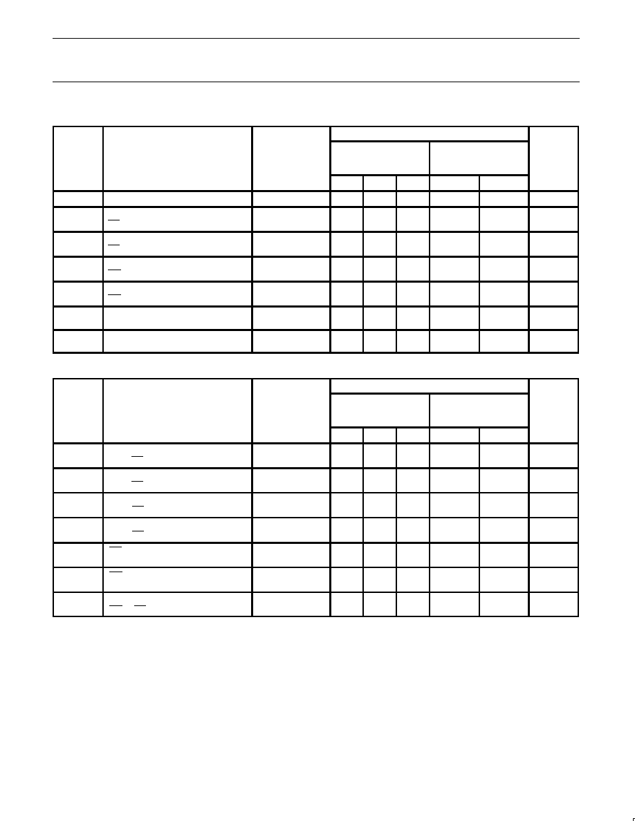
ABSOLUTE MAXIMUM RATINGS
(Operation beyond the limits set forth in this table may impair the useful life of the device.
Unless otherwise noted these limits are over the operating free-air temperature range.)
SYMBOL
PARAMETER
RATING
UNIT
V
CC
Supply voltage
≠0.5 to +7.0
V
V
IN
Input voltage
≠0.5 to +7.0
V
I
IN
Input current
≠30 to +5
mA
V
OUT
Voltage applied to output in High output state
≠0.5 to +5.5
V
I
OUT
Current applied to output in Low output state
Qs
40
mA
I
OUT
Current applied to output in Low output state
Q0≠Q3
48
mA
T
amb
Operating free-air temperature range
0 to +70
∞
C
T
stg
Storage temperature range
≠65 to +150
∞
C
RECOMMENDED OPERATING CONDITIONS
SYMBOL
PARAMETER
LIMITS
UNIT
SYMBOL
PARAMETER
MIN
NOM
MAX
UNIT
V
CC
Supply voltage
4.5
5.0
5.5
V
V
IH
High-level input voltage
2.0
V
V
IL
Low-level input voltage
0.8
V
I
IK
Input clamp current
≠18
mA
I
OH
High-level output current
Qs
≠1
mA
I
OH
High-level output current
Q0≠Q3
≠3
mA
I
OL
Low-level output current
Qs
20
mA
I
OL
Low-level output current
Q0≠Q3
24
mA
T
amb
Operating free-air temperature range
0
70
∞
C
Philips Semiconductors
Product specification
74F395
4-bit cascadable shift register (3-State)
1990 Oct 23
4
DC ELECTRICAL CHARACTERISTICS
(Over recommended operating free-air temperature range unless otherwise noted.)
SYMBOL
PARAMETER
TEST CONDITIONS
1
LIMITS
UNIT
SYMBOL
PARAMETER
TEST CONDITIONS
1
MIN
TYP
2
MAX
UNIT
V
OH
High-level output voltage
Qs
V
CC
= MIN,
V
IL
= MAX,
V
IH
=MIN
I
OH
=≠1mA
±
10%V
CC
2.5
V
V
OH
High-level output voltage
Qs
V
CC
= MIN,
V
IL
= MAX,
V
IH
=MIN
I
OH
=≠1mA
±
5%V
CC
2.7
3.4
V
V
OH
High-level output voltage
Q0≠Q3
V
IL
= MAX,
V
IH
=MIN
I
OH
=≠3mA
±
10%V
CC
2.4
V
Q0≠Q3
IH
=MIN
I
OH
=≠3mA
±
5%V
CC
2.7
V
V
OL
Low-level output voltage
V
CC
= MIN,
V
IL
= MAX,
V
IH
= MIN,
I
OL
= MAX
±
10%V
CC
0.35
0.50
V
V
OL
Low-level output voltage
V
IL
= MAX,
V
IH
= MIN,
I
OL
= MAX
±
5%V
CC
0.35
0.50
V
V
IK
Input clamp voltage
V
CC
= MIN, I
I
= I
IK
≠0.73
≠1.2
V
I
I
Input current at maximum input voltage
V
CC
= MAX, V
I
= 7.0V
100
µ
A
I
IH
High-level input current
V
CC
= MAX, V
I
= 2.7V
20
µ
A
I
IL
Low-level input current
V
CC
= MAX, V
I
= 0.5V
≠0.6
mA
I
OZH
Off-state output current High
level of voltage applied
Q0≠Q3
only
V
CC
= MAX, V
O
= 2.7V
50
µ
A
I
OZL
Off-state output current Low
level of voltage applied
Q0≠Q3
only
V
CC
= MAX, V
O
= 0.5V
≠50
µ
A
I
OS
Short-circuit output current
3
V
CC
= MAX
≠60
≠150
mA
I
CC
Supply current (total)
I
CCH
V
CC
= MAX
MR=PE=Dn=Ds=4.5V,
OE=GND, CP=
#
33
48
mA
I
CC
Supply current (total)
I
CCL
V
CC
= MAX
MR=OE=Dn=Ds=GND,
PE=4.5V, CP=
#
35
50
mA
I
CCZ
MR=Dn=Ds=GND,
OE=4.5V
32
46
mA
NOTES:
1. For conditions shown as MIN or MAX, use the appropriate value specified under recommended operating conditions for the applicable type.
2. All typical values are at V
CC
= 5V, T
amb
= 25
∞
C.
3. Not more than one output should be shorted at a time. For testing I
OS
, the use of high-speed test apparatus and/or sample-and-hold
techniques are preferable in order to minimize internal heating and more accurately reflect operational values. Otherwise, prolonged shorting
of a High output may raise the chip temperature well above normal and thereby cause invalid readings in other parameter tests. In any
sequence of parameter tests, I
OS
tests should be performed last.
Philips Semiconductors
Product specification
74F395
4-bit cascadable shift register (3-State)
1990 Oct 23
5
AC ELECTRICAL CHARACTERISTICS
SYMBOL
PARAMETER
TEST
CONDITION
LIMITS
UNIT
SYMBOL
PARAMETER
TEST
CONDITION
V
CC
= +5V
T
amb
= +25
∞
C
C
L
= 50pF, R
L
= 500
V
CC
= +5V
±
10%
T
amb
= 0
∞
C to +70
∞
C
C
L
= 50pF, R
L
= 500
UNIT
MIN
TYP
MAX
MIN
MAX
f
MAX
Maximum clock frequency
Waveform 1
105
120
MHz
t
PLH
t
PHL
Propagation delay
CP to Qn
Waveform 1
3.5
5.0
6.0
8.0
8.5
11.0
3.5
5.0
9.5
11.5
ns
t
PLH
t
PHL
Propagation delay
CP to Qs
Waveform 1
4.5
5.5
6.0
7.5
8.5
10.0
4.0
5.0
9.5
10.5
ns
t
PHL
Propagation delay
MR to Qn
Waveform 2
5.0
7.5
10.0
5.0
10.5
ns
t
PHL
Propagation delay
MR to Qs
Waveform 2
4.5
7.0
9.0
4.5
9.5
ns
t
PZH
t
PZL
Output Enable time
to High or Low level
Waveform 4
Waveform 5
4.0
3.5
6.5
6.0
9.0
8.0
4.0
3.5
10.0
8.5
ns
t
PHZ
t
PLZ
Output Disable time
from High or Low level
Waveform 4
Waveform 5
1.0
1.0
2.5
3.5
4.5
5.5
1.0
1.0
5.5
6.5
ns
AC SETUP REQUIREMENTS
SYMBOL
PARAMETER
TEST
CONDITION
LIMITS
UNIT
SYMBOL
PARAMETER
TEST
CONDITION
V
CC
= +5V
T
amb
= +25
∞
C
C
L
= 50pF, R
L
= 500
V
CC
= +5V
±
10%
T
amb
= 0
∞
C to +70
∞
C
C
L
= 50pF, R
L
= 500
UNIT
MIN
TYP
MAX
MIN
MAX
t
s
(H)
t
s
(L)
Setup time, High or Low
Dn to CP
Waveform 3
2.5
1.5
3.0
2.0
ns
t
h
(H)
t
h
(L)
Hold time, High or Low
Dn to CP
Waveform 3
1.5
1.5
1.5
1.5
ns
t
s
(H)
t
s
(L)
Setup time, High or Low
PE to CP
Waveform 3
6.5
6.0
7.0
6.5
ns
t
h
(H)
t
h
(L)
Hold time, High or Low
PE to CP
Waveform 3
0
0
0
0
ns
t
W
(H)
t
W
(L)
CP Pulse width
High or Low
Waveform 1
5.0
4.0
5.5
4.5
ns
t
W
(L)
MR Pulse width
Low
Waveform 2
2.5
3.0
ns
t
REC
Recovery time
MR to CP
Waveform 2
6.0
7.0
ns

Philips Semiconductors
Product specification
74F395
4-bit cascadable shift register (3-State)
1990 Oct 23
6
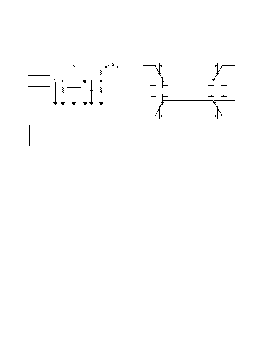
AC WAVEFORMS
For all waveforms, V
M
= 1.5V.
The shaded areas indicate when the input is permitted to change for predictable output performance.
V
M
V
M
V
M
1/f
MAX
t
PHL
t
w
(L)
Qn, Qs
t
w
(H)
V
M
CP
t
PLH
SF00944
Waveform 1. Propagation Delay, Clock Input to Output,
Clock Widths, and Maximum Clock Frequency
VM
VM
VM
tREC
tPHL
MR
CP
Qn, Qs
VM
tw(L)
SF00945
Waveform 2. Master Reset Pulse Width, Master Reset to
Output Delay, and Master Reset to Clock Recovery Time
SF00946
V
M
V
M
V
M
V
M
V
M
V
M
PE
CP
V
M
V
M
Dn
t
s
t
h
V
M
V
M
t
s
t
h
t
s
t
h
t
s
t
h
Ds
STABLE
STABLE
Waveform 3. Parallel Enable and
Data Setup Time and Hold Time
VM
VM
VM
tPHZ
tPZH
VOH -0.3V
0V
OE
Qn
SF00343
Waveform 4. 3-State Output Enable Time to High Level and
Output Disable Time from High Level
VM
VM
VM
tPLZ
tPZL
VOL +0.3V
Qn
OE
SF00344
Waveform 5. 3-State Output Enable Time to Low Level and
Output Disable Time from Low Level
Philips Semiconductors
Product specification
74F395
4-bit cascadable shift register (3-State)
1990 Oct 23
7
TEST CIRCUIT AND WAVEFORMS
tw
90%
VM
10%
90%
VM
10%
90%
VM
10%
90%
VM
10%
NEGATIVE
PULSE
POSITIVE
PULSE
tw
AMP (V)
0V
0V
tTHL (tf
)
INPUT PULSE REQUIREMENTS
rep. rate
t
w
t
TLH
t
THL
1MHz
500ns
2.5ns
2.5ns
Input Pulse Definition
VCC
family
74F
D.U.T.
PULSE
GENERATOR
RL
CL
RT
VIN
VOUT
Test Circuit for 3-State Outputs and
Totem-Pole Output (Qs)
DEFINITIONS:
R
L
= Load resistor;
see AC electrical characteristics for value.
C
L
= Load capacitance includes jig and probe capacitance;
see AC electrical characteristics for value.
R
T
= Termination resistance should be equal to Z
OUT
of
pulse generators.
tTHL (tf
)
tTLH (tr
)
tTLH (tr
)
AMP (V)
amplitude
3.0V
1.5V
V
M
RL
7.0V
SF00957
TEST
SWITCH
t
PLZ
closed
t
PZL
closed
All other
open
SWITCH POSITION