 | –≠–ª–µ–∫—Ç—Ä–æ–Ω–Ω—ã–π –∫–æ–º–ø–æ–Ω–µ–Ω—Ç: N74F410N | –°–∫–∞—á–∞—Ç—å:  PDF PDF  ZIP ZIP |
Document Outline
- FEATURES
- DESCRIPTION
- FUNCTIONAL DESCRIPTION
- ORDERING INFORMATION
- INPUT AND OUTPUT LOADING AND FAN OUT TABLE
- PIN CONFIGURATION
- LOGIC SYMBOL
- IEC/IEEE SYMBOL
- LOGIC DIAGRAM
- ABSOLUTE MAXIMUM RATINGS
- RECOMMENDED OPERATING CONDITIONS
- DC ELECTRICAL CHARACTERISTICS
- AC ELECTRICAL CHARACTERISTICS
- AC SETUP REQUIREMENTS FOR READ MODE
- AC SETUP REQUIREMENTS FOR WRITE MODE
- AC WAVEFORMS
- TEST CIRCUIT AND WAVEFORM
Philips Semiconductors FAST Products
Product specification
74F410
Register stack ≠ 16
◊
4 RAM 3-State output register
1
January 8, 1990
853-1310 98498
FEATURES
∑
Edge triggered output register
∑
ypical access time of 19.5ns
∑
Optimize for register stack operation
∑
3≠state outputs
∑
18≠pin package
DESCRIPTION
The 74F410 is a register oriented high speed
64≠bit read/write memory organized as
16≠words by 4≠bits. An edge≠triggered 4≠bit
output register allows new input data to be
written while previous data is held. 3≠state
outputs are provided for maximum versatility.
The 74F410 is fully compatible with all TTL
families.
TYPE
TYPICAL
ACCESS
TIME
TYPICAL
SUPPLY
CURRENT
( TOTAL)
74F410
19.5ns
45mA
FUNCTIONAL DESCRIPTION
Write operation ≠ When the three control
inputs, write enable (WE), chip select (CS),
and clock (CP), are low the information on
the data inputs (D0≠D3) is written into the
memory location selected by the address
inputs (A0≠A3). If the input data changes
while WE, CS, and CP are low, the contents
of the selected memory location follow these
changes provided setup and hold time criteria
are met.
Read operation ≠ When CS is low, WE is
high, and CP goes from low≠to≠high, the
contents of the memory location selected by
the address inputs (A0≠A3) are edge≠
triggered into the output register.
When WE is low, CS is low, CP goes from
low≠to≠high, the data at the data inputs is
edge≠triggered into the output register. The
OE input controls the output buffers. When
OE is high the four outputs (Q0≠Q3) are in a
high impedance or off state; when OE is low,
the outputs are determined by the state of the
output register.
ORDERING INFORMATION
ORDER CODE
DESCRIPTION
COMMERCIAL RANGE
V
CC
= 5V
±
10%, T
amb
= 0
∞
C to +70
∞
C
18≠pin plastic DIP (300mil)
N74F410N
INPUT AND OUTPUT LOADING AND FAN OUT TABLE
PINS
DESCRIPTION
74F (U.L.)
HIGH/LOW
LOAD VALUE
HIGH/LOW
D0 ≠ D3
Data inputs
1.0/1.0
20
µ
A
/
0.6mA
A0 ≠ A3
Address inputs
1.0/1.0
20
µ
A
/
0.6mA
CP
Clock pulse input (active rising edge)
1.0/2.0
20
µ
A/1.2mA
CS
Chip select input (active low)
1.0/2.0
20
µ
A/1.2mA
OE
Output enable input (active low)
1.0/1.0
20
µ
A/0.6mA
WE
Write enable input (active low)
1.0/1.0
20
µ
A/0.6mA
Q0 ≠ Q3
Data outputs
150/40
3mA/24mA
NOTE: One (1.0) FAST unit load is defined as: 20
µ
A in the high state and 0.6mA in the low state.
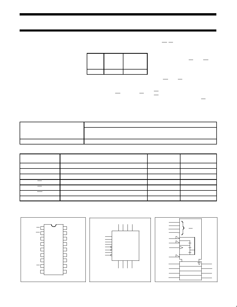
PIN CONFIGURATION
LOGIC SYMBOL
IEC/IEEE SYMBOL
18
17
16
15
14
13
12
7
6
5
4
3
2
1
A1
Q1
Q2
D3
D2
D0
Q0
CS
WE
CP
A0
A3
OE
3
4
5
6
11
10
D0
D2 D3
D1
Q0 Q1 Q2 Q3
16 14 12 10
15 13 11
11
8
A2
VCC
VCC = Pin 18
GND = Pin 9
D1
17
A0
A1
A2
A3
CS
WE
CP
OE
3
4
5
6
1
2
7
8
13
12
15
14
17
16
2
1
A1,2D
A3
&
0
1
A
0
15
Q3
GND
10
9
7
8
&
G1
G2
1C
EN3
Philips Semiconductors FAST Products
Product specification
74F410
Register stack ≠ 16
◊
4 RAM 3-State output register
January 8, 1990
2
LOGIC DIAGRAM
VCC
=
pin
18
GND = pin 9
Address
decoder
A0
A1
A2
A3
3
4
5
6
RAM
16
4
D0
D1
D2
D3
17
15
13
11
Data
inputs
16
Register
Q0
Q1
Q2
Q3
16
14
12
10
WE
CS
CP
OE
8
15
13
11
ABSOLUTE MAXIMUM RATINGS
(Operation beyond the limit set forth in this table may impair the useful life of the device. Unless otherwise noted these limits are over the
operating free air temperature range.)
SYMBOL
PARAMETER
RATING
UNIT
V
CC
Supply voltage
≠0.5 to +7.0
V
V
IN
Input voltage
≠0.5 to +7.0
V
I
IN
Input current
≠30 to +5
mA
V
OUT
Voltage applied to output in high output state
≠0.5 to V
CC
V
I
OUT
Current applied to output in low output state
48
mA
T
amb
Operating free air temperature range
0 to +70
∞
C
T
stg
Storage temperature range
≠65 to +150
∞
C
Philips Semiconductors FAST Products
Product specification
74F410
Register stack ≠ 16
◊
4 RAM 3-State output register
January 8, 1990
3
RECOMMENDED OPERATING CONDITIONS
SYMBOL
PARAMETER
LIMITS
T
A
=
≠
4
0
t
o
+
8
5
∞
C
UNIT
MIN
NOM
MAX
V
CC
Supply voltage
4.5
5.0
5.5
V
V
IH
High≠level input voltage
2.0
V
V
IL
Low≠level input voltage
0.8
V
I
Ik
Input clamp current
≠18
mA
I
OH
High≠level output current
≠3
mA
I
OL
Low≠level output current
24
mA
T
amb
Operating free air temperature range
0
+70
∞
C
DC ELECTRICAL CHARACTERISTICS
(Over recommended operating free-air temperature range unless otherwise noted.)
SYMBOL
PARAMETER
TEST CONDITIONS
1
LIMITS
UNIT
MIN
TYP
2
MAX
V
OH
High-level output voltage
V
CC
= MIN, V
IL
= MAX
±
10%V
CC
2.4
V
V
IH
= MIN, I
OH
= MAX
±
5%V
CC
2.7
V
V
OL
Low-level output voltage
V
CC
= MIN, V
IL
= MAX
±
10%V
CC
0.35
0.50
V
V
IH
= MIN, I
OL
= MAX
±
5%V
CC
0.35
0.50
V
V
IK
Input clamp voltage
V
CC
= MIN, I
I
= I
IK
-0.73
-1.2
V
I
I
Input current at maximum input voltage
V
CC
= MAX, V
I
= 7.0V
100
µ
A
I
IH
High≠level input current
V
CC
= MAX, V
I
= 2.7V
20
µ
A
I
IL
Low≠level input current
others
V
CC
= MAX, V
I
= 0.5V
-0.6
mA
CP, CS
-1.2
mA
I
OZH
Offset≠output current,
high≠level voltage applied
V
CC
= MAX, V
I
= 2.7V
50
µ
A
I
OZL
Offset≠output current,
low≠level voltage applied
V
CC
= MAX, V
I
= 0.5V
≠50
µ
A
I
OS
Short-circuit output current
3
V
CC
= MAX
-60
-150
mA
I
CC
Supply current (total)
V
CC
= MAX
45
70
mA
NOTES:
1. For conditions shown as MIN or MAX, use the appropriate value specified under recommended operating conditions for the applicable type.
2. All typical values are at V
CC
= 5V, T
amb
= 25
∞
C.
3. Not more than one output should be shorted at a time. For testing I
OS
, the use of high-speed test apparatus and/or sample-and-hold
techniques are preferable in order to minimize internal heating and more accurately reflect operational values. Otherwise, prolonged shorting
of a high output may raise the chip temperature well above normal and thereby cause invalid readings in other parameter tests. In any
sequence of parameter tests, I
OS
tests should be performed last.
Philips Semiconductors FAST Products
Product specification
74F410
Register stack ≠ 16
◊
4 RAM 3-State output register
January 8, 1990
4
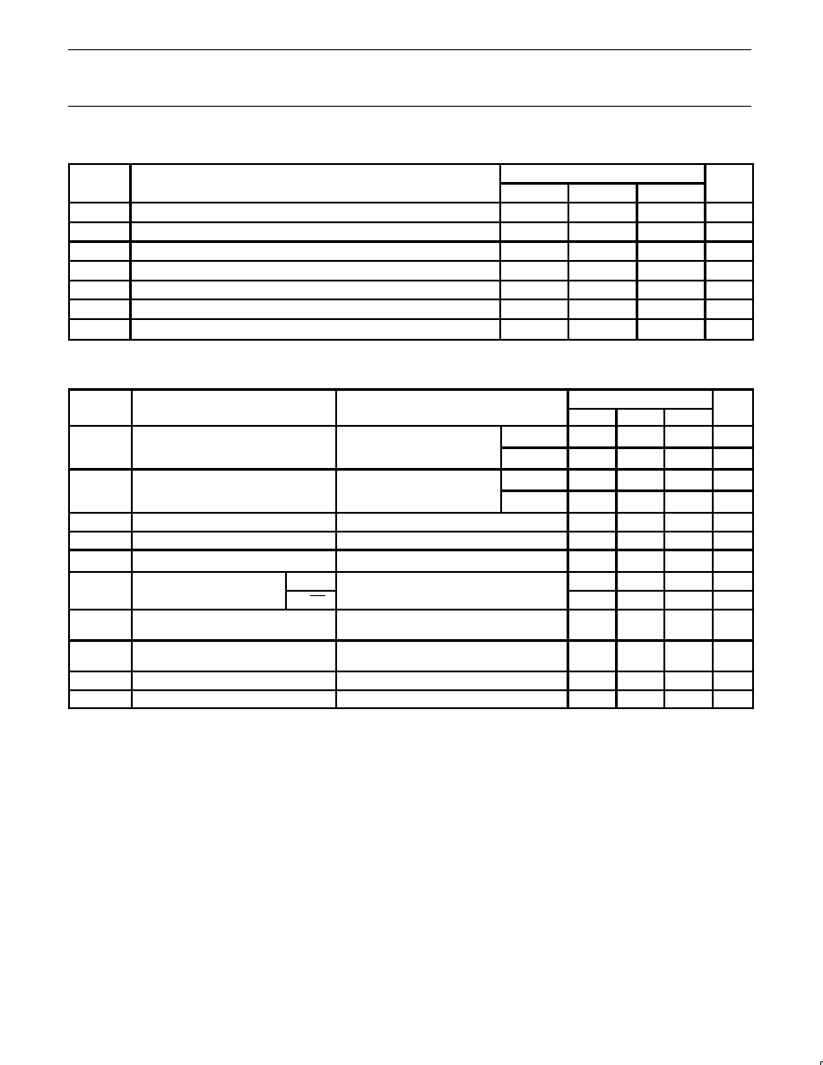
AC ELECTRICAL CHARACTERISTICS
LIMITS
T
amb
= +25
∞
C
T
amb
= 0
∞
C to +70
∞
C
SYMBOL
PARAMETER
TEST
V
CC
= +5.0V
V
CC
= +5.0V
±
10%
UNIT
CONDITION
C
L
= 50pF, R
L
= 500
C
L
= 50pF, R
L
= 500
MIN
TYP
MAX
MIN
MAX
t
PLH
t
PHL
Propagation dealy
CP to Qn
Waveform 1
4.0
4.5
6.5
6.5
8.5
9.0
3.5
4.0
9.5
10.0
ns
t
PZH
t
PZL
Output enable time
OE to Qn
Waveform 3, 4
3.0
4.5
4.5
6.0
7.5
9.0
2.5
3.5
8.5
9.5
ns
t
PHZ
t
PHL
Output disable time
OE to Qn
Waveform 3, 4
2.0
2.0
3.5
3.5
6.0
6.5
1.5
2.0
6.5
7.0
ns
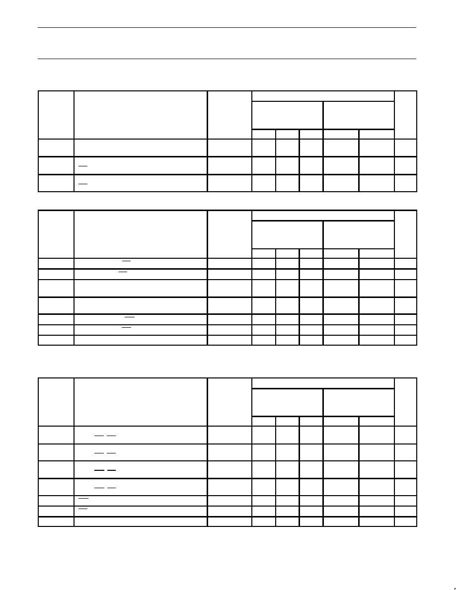
AC SETUP REQUIREMENTS FOR READ MODE
LIMITS
T
amb
= +25
∞
C
T
amb
= 0
∞
C to +70
∞
C
SYMBOL
PARAMETER
TEST
V
CC
= +5.0V
V
CC
= +5.0V
±
10%
UNIT
CONDITION
C
L
= 50pF, R
L
= 500
C
L
= 50pF, R
L
= 500
MIN
TYP
MAX
MIN
MAX
t
su
(L)
Setup time, low, CS to CP
1
Waveform 1
4.0
4.5
ns
t
h
(L)
Hold time, low, CS to CP
1
Waveform 1
3.5
4.5
ns
t
su
(H)
t
su
(L)
Setup time, high or low
An to CP
1
Waveform 1
13.0
13.0
15.0
15.0
ns
t
h
(H)
t
h
(L)
Hold time, high or low
An to CP
1
Waveform 1
0
0
0
0
ns
t
su
(H)
Setup time, high, WE to CP
1
Waveform 1
13.0
15.0
ns
t
h
(H)
Hold time, high, WE to CP
1
Waveform 1
0
0
ns
t
w
(L)
CP pulse width, low
Waveform 1
5.0
6.0
ns
NOTE:
1. Low≠to≠high clock transition.
AC SETUP REQUIREMENTS FOR WRITE MODE
LIMITS
T
amb
= +25
∞
C
T
amb
= 0
∞
C to +70
∞
C
SYMBOL
PARAMETER
TEST
V
CC
= +5.0V
V
CC
= +5.0V
±
10%
UNIT
CONDITION
C
L
= 50pF, R
L
= 500
C
L
= 50pF, R
L
= 500
MIN
TYP
MAX
MIN
MAX
t
su
(H)
t
su
(L)
Setup time, high or low
An to WE, CS, CP
Waveform 2
0
0
0
0
ns
t
h
(H)
t
h
(L)
Hold time, high or low
An to WE, CS, CP
Waveform 2
0
0
0
0
ns
t
su
(H)
t
su
(L)
Setup time, high or low
Dn to WE, CS, CP
Waveform 2
6.0
6.0
8.0
8.0
ns
t
h
(H)
t
h
(L)
Hold time, high or low
Dn to WE, CS, CP
Waveform 2
0
0
0
0
ns
t
w
(L)
WE pulse width, low
Waveform 2
7.0
8.0
ns
t
w
(L)
CS pulse width, low
Waveform 2
6.0
7.0
ns
t
w
(L)
CP pulse width, low
Waveform 2
7.0
8.0
ns
Philips Semiconductors FAST Products
Product specification
74F410
Register stack ≠ 16
◊
4 RAM 3-State output register
January 8, 1990
5
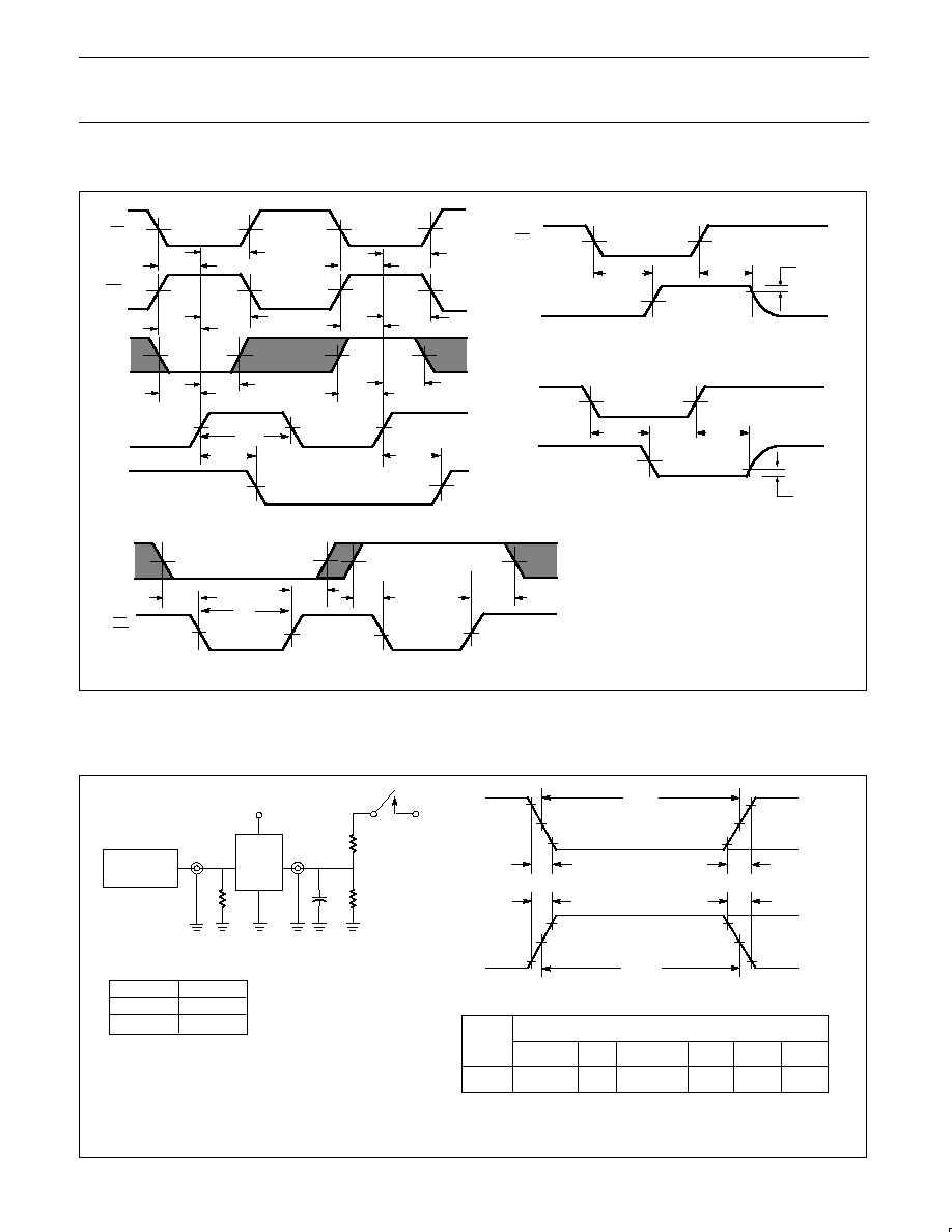
AC WAVEFORMS
Waveform 1. Read cycle timing
CP
VM
VM
VM
VM
VM
VM
tsu(H)
th(H)
An
VM
tw(H)
tsu(L)
th(L)
VM
VM
Qn
tw(L)
tPLH
Waveform 2. Write cycle timing
WE
VM
VM
VM
VM
VM
VM
CS
tsu(H)
th(H)
tsu(L)
th(L)
tsu(L)
th(L)
VM
tsu(H)
th(H)
VM
VM
VM
VM
VM
tsu(H)
th(H)
An,
Dn
tsu(L)
th(L)
VM
VM
VM
VM
CS
WE
CP
Waveform 3. 3-State output enable time to high level
and output disable time from high level
VM
VM
VM
tPHZ
tPZH
VOH -0.3V
0V
OE
Qn
Waveform 4. 3-State output enable time to low level
and output disable time from low level
VM
VM
VM
tPLZ
tPZL
VOL +0.3V
Qn
OE
tPHL
NOTES:
1. For all waveforms, V
M
= 1.5V.
2. The shaded areas indicate when the input is permitted to change for predictable output performance.
TEST CIRCUIT AND WAVEFORM
tW
90%
VM
10%
90%
VM
10%
90%
VM
10%
90%
VM
10%
NEGATIVE
PULSE
POSITIVE
PULSE
tW
AMP (V)
0V
0V
tTHL (tf
)
INPUT PULSE REQUIREMENTS
rep. rate
t
W
t
TLH
t
THL
1MHz
500ns 2.5ns
2.5ns
Input pulse definition
VCC
family
74F
D.U.T.
PULSE
GENERATOR
RL
CL
RT
VIN
VOUT
Test circuit for 3≠state outputs
DEFINITIONS:
R
L
= Load resistor; see AC electrical characteristics for
value.
C
L
= Load capacitance includes jig and probe
capacitance; see AC electrical characteristics for
value
R
T
= Termination resistance should be equal to Z
OUT
of
pulse generators.
tTHL (tf
)
tTLH (tr
)
tTLH (tr
)
AMP (V)
amplitude
3.0V
1.5V
V
M
RL
7.0V
SWITCH POSITION
TEST
SWITCH
closed
open
All other
t
PLZ
, t
PZL