 | –≠–ª–µ–∫—Ç—Ä–æ–Ω–Ω—ã–π –∫–æ–º–ø–æ–Ω–µ–Ω—Ç: N74F524N | –°–∫–∞—á–∞—Ç—å:  PDF PDF  ZIP ZIP |
Philips
Semiconductors
74F524
8-bit register comparator (open-collector
+ 3-State)
Product specification
IC15 Data Handbook
1990 Aug 07
INTEGRATED CIRCUITS

Philips Semiconductors
Product specification
74F524
8-bit register comparator (open collector + 3-State)
2
1990 Aug 07
853≠0373 00135
FEATURES
∑
8-Bit bidirectional register with bus-oriented input-output
∑
Independent serial input-output to register
∑
Register bus comparator with `equal to', `greater than' and
`less than' outputs
∑
Cascadable in groups of 8-bits
∑
Open collector comparator outputs for AND-wired expansion
∑
Two's complement or magnitude compare
DESCRIPTION
The 74F524 is an 8-bit bidirectional register with parallel input and
output, plus serial input and output progressing from MSB to LSB.
All data inputs, serial and parallel, are loaded by the rising edge of
the clock. The device functions are controlled by two control lines
(S0, S1) to execute shift, load, hold and read out. An 8-bit
comparator examines the data stored in the registers and on the
data bus. Three true-High, open collector outputs representing
`register equal to bus', `register greater than bus' and `register less
than bus' are provided. These outputs can be disabled to the OFF
state by the use of Status Enable (SE). A mode control has also
been provided to allow Two's Complement as well as magnitude
compare. Linking inputs are provided for expansion to longer words.
PIN CONFIGURATION
20
19
18
17
16
15
14
13
12
11
10
9
8
7
6
5
4
3
2
1
S0
I/O0
I/O1
I/O2
I/O3
I/O4
I/O6
I/O7
GND
CP
M
LT
C/SO
C/SI
SE
S1
V
CC
EQ
GT
I/O5
SF00970
TYPE
TYPICAL f
MAX
TYPICAL SUPPLY CURRENT
(TOTAL)
74F524
65MHz
110mA
ORDERING INFORMATION
DESCRIPTION
COMMERCIAL
RANGE
V
CC
= 5V
±
10%,
T
amb
= 0
∞
C to +70
∞
C
PKG DWG #
20-pin plastic DIP
N74F524N
SOT146-1
20-pin plastic SOL
N74F524D
SOT163-1
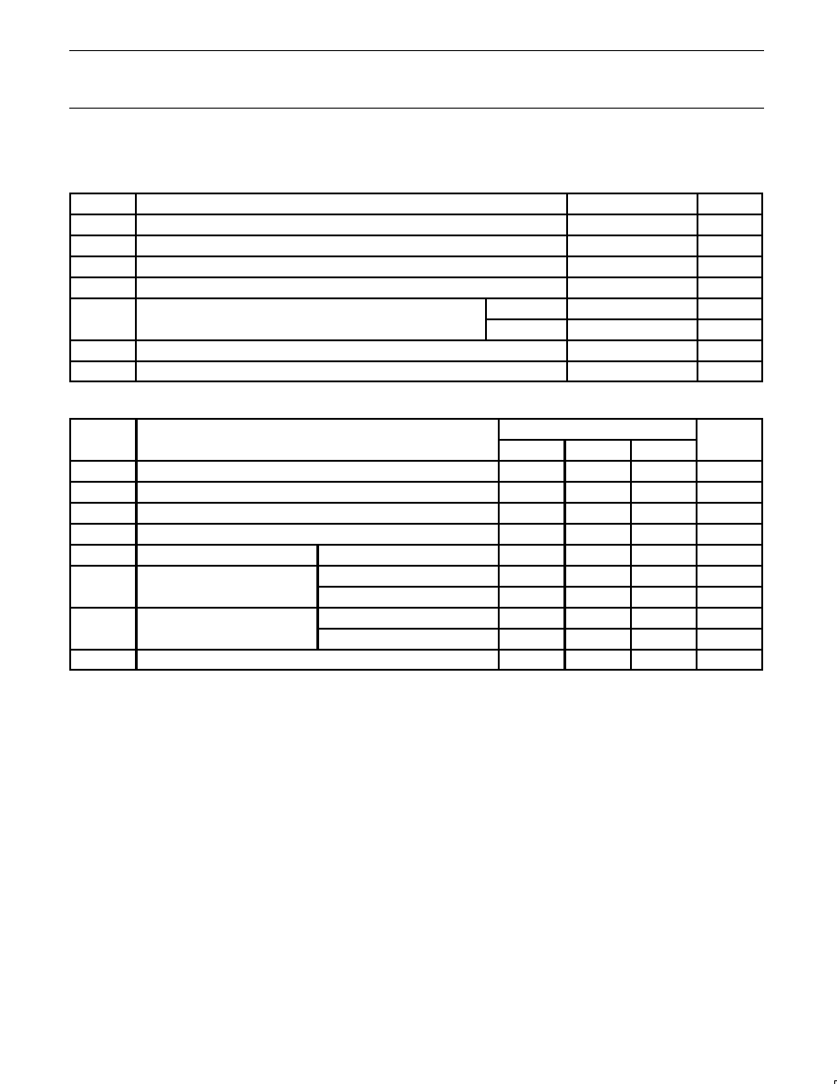
INPUT AND OUTPUT LOADING AND FAN-OUT TABLE
PINS
DESCRIPTION
74F(U.L.)
HIGH/LOW
LOAD VALUE
HIGH/LOW
I/On
Parallel data inputs
3.5/1.0
70
µ
A/0.6mA
S0, S1
Mode select inputs
1.0/1.0
20
µ
A/0.6mA
C/SI
Status priority or serial data input
1.0/1.0
20
µ
A/0.6mA
CP
Clock pulse input (active rising edge)
1.0/1.0
20
µ
A/0.6mA
SE
Status enable input (active Low)
1.0/1.0
20
µ
A/0.6mA
M
Compare mode select input
1.0/1.0
20
µ
A/0.6mA
I/On
3-state parallel data outputs
150/40
3.0mA/24mA
C/SO
Status priority or serial data output
50/33
1.0mA/20mA
LT
Register less than bus output
OC/33
OC/20mA
EQ
Register equal to bus output
OC/33
OC/20mA
GT
Register greater than bus output
OC/33
OC/20mA
NOTE:
One (1.0) FAST Unit Load (U.L.) is defined as 20
µ
A in the High state and 0.6mA in the Low state.
OC=Open Collector
Philips Semiconductors
Product specification
74F524
8-bit register comparator (open collector + 3-State)
1990 Aug 07
3
LOGIC SYMBOL for 74F456
M
SE
I/O0
I/O1 I/O2 I/O3 I/O4 I/O5 I/O6 I/O7
S1
CP
S0
12
18
19
11
1
2
3
4
5
6
7
8
9
SF00971
V
CC
= Pin 20
GND = Pin 10
C/SI
17
GT
EQ
LT
14
15
13
C/SO
16
LOGIC SYMBOL (IEEE/IEC) for 74F456
SF00972
&
G7
1
2
3
5
6
7
8
9
11
18
17
13
COMP
19
12
0
3
M
0
1
4
3, 4D
14
15
16
2D
1,5,6,7>I/O
1,5,6,7<I/O
1,5,6,7=I/O
M6 TWO's COMPLEMENT
M5 MAGNITUDE
C4/2/4
0=HOLD
1=READ
2=SHIFT
3=LOAD
FUNCTIONAL DESCRIPTION
The 74F524 contains eight D-type flip-flops connected as a shift
register with provision for either parallel or serial loading. Parallel
data may be read from or loaded into the registers via the data bus
I/O0≠I/O7. Serial data is loaded into the register from the C/SI input
and may be shifted through the register and out through the C/SO
output. Both parallel and serial data entry occurs on the rising edge
of the clock (CP). The operation of the shift register is controlled by
two signals, S0 and S1, according to the Select Function Table. The
3-State parallel output buffers are enabled only in the READ mode.
SELECT FUNCTION TABLE
S0
S1
OPERATION
L
L
HOLD≠Retains data in shift register
L
H
READ≠Read contents in register onto data bus
H
L
SHIFT≠Allows serial shifting on next rising clock
edge
H
H
LOAD≠Load data on bus into register
H = High voltage level
L
= Low voltage level
One port of an 8-bit comparator is attached to the data bus while the
other port is tied to the outputs of the internal register. Three
active-OFF Open Collector outputs indicate whether the contents
held in the shift register are `greater than' (GT). `less than' (LT), or
`equal to' (EQ) the data on the input bus. A High signal on the Status
Enable (SE) input disables these outputs to the OFF state. A mode
control (M) input allows selection between a straightforward
magnitude compare or a comparison between Two's complement
numbers.
NUMBER REPRESENTATION SELECT TABLE
M
OPERATION
L
Magnitude compare
H
Two's Complement compare
H = High voltage level
L
= Low voltage level
For `greater than' or `less than' detection, the C/SI input must be
held High, as indicated in the Function Table. The internal logic is
arranged such that a Low signal on the C/SI input places the
`greater than' and `less than' outputs in their off state. (Note that this
off state serves also as the active state when C/SI is High. It is
intended for use in expansion to word lengths greater than 8 bits
using multiple 74S524s as explained in the next 3 paragraphs.) The
C/SO output will be forced High if the `equal to' status condition
exists; otherwise, C/SO will be held Low.
Word length expansion (in groups of 8 bits) can be achieved by
connecting the C/SO output of the more significant byte to the C/SI
input of the next less significant byte and also to its own SE input
(see Application Figure 1). The CS/I input of the most significant
device is held High while the SE input of the least significant device
is held Low. The corresponding status outputs are AND-wired
together. In the case of two's complement number compare, only the
Mode input to the most significant device should be High. the Mode
inputs to all other cascaded devices are held Low.
Suppose that an inequality condition is detected in the most
significant device. Assuming that the byte stored in the register is
greater than the byte on the data bus, then the EQ and LT outputs
will be pulled Low, whereas the GT output will float High. Also, the
Philips Semiconductors
Product specification
74F524
8-bit register comparator (open collector + 3-State)
1990 Aug 07
4
CS/O output of the most significant device will be forced Low,
disabling the subsequent devices but enabling its own status
outputs. The corrected status condition is thus indicated. The same
applies if the register byte is less than the data byte, only in this
case the EQ and GT outputs go Low, whereas the LT output floats
High.
If an equality condition is detected in the most significant device, its
C/SO output is forced High. This enables the next less significant
device and disables its own status outputs. In this way, the status
output proximity is handed down to the next less significant device
which now effectively becomes the most significant byte. The worst
case propagation delay for a compare operation involving `n'
cascaded 74F524s will be when an equality condition is detected in
all but the least significant byte. In this case, the status priority has
to ripple all the way down the chain before the correct status output
is established. Typically, this will take 35+6(n≠2) ns.
APPLICATION
C/SI
M
GT
EQ
LT
S0
S1
I/O
SE
C/SO
H
C/SI
M
GT
EQ
LT
S0
S1
I/O
SE
C/SO
C/SI
M
GT
EQ
LT
S0
S1
I/O
SE
C/SO
RD
WR
MSB
8
8
8
LSB
L
L
L
H = TWO's COMPLEMENT
L = MAGNITUDE
GREATER THAN
EQUAL TO
LESS THAN
V
CC
SF01012
Figure 1. Cascading 74F524s for Comparing Longer Words
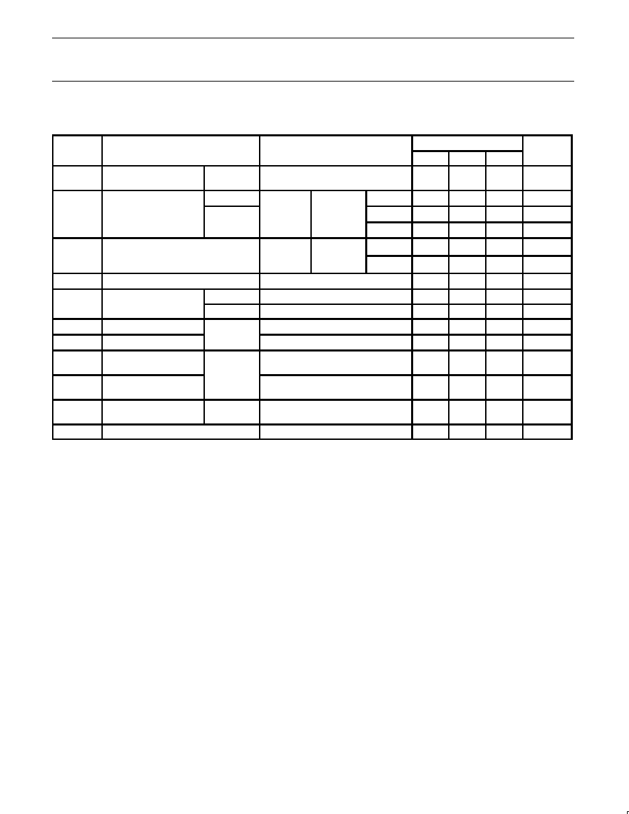
FUNCTION TABLE
INPUTS
OUTPUTS
OPERATING MODE
SE
C/SI
S0
S1
Data comparison
EQ
GT
LT
C/SO
OPERATING MODE
H
H
L
L
X
H
H
H
(1)
Hold
H
L
L
L
X
H
H
H
L
Hold
H
X
H
L
X
H
H
H
Q0
Shift
H
H
L
H
X
H
H
H
(1)
Read
H
L
L
H
X
H
H
H
L
Read
H
H
H
H
X
H
H
H
(1)
Load
H
L
H
H
X
H
H
H
L
Load
L
L
H or L
2
H or L
2
OA≠OH > I/O0≠I/O7
L
H
H
L
L
L
H or L
2
H or L
2
OA≠OH = I/O0≠I/O7
H
H
H
L
Compare
(GT=CT=off)
L
L
H or L
2
H or L
2
OA≠OH < I/O0≠I/O7
L
H
H
L
(GT=CT=off)
L
H
H or L
2
H or L
2
OA≠OH > I/O0≠I/O7
L
H
L
L
L
H
H or L
2
H or L
2
OA≠OH = I/O0≠I/O7
H
L
L
H
Compare
(GT=CT=on)
L
H
H or L
2
H or L
2
OA≠OH < I/O0≠I/O7
L
L
H
L
(GT=CT=on)
(1) = High if I/On=Dn, otherwise Low
2
= Must meet setup and hold time requirements
H = High voltage level
L
= Low voltage level
X = Don't care
Philips Semiconductors
Product specification
74F524
8-bit register comparator (open collector + 3-State)
1990 Aug 07
5
LOGIC DIAGRAM
16
15
14
13
SF00973
VCC = Pin 20
GND = Pin 10
CP
D
Q
Q
CP
D
Q
Q
CP
D
Q
Q
CP
D
Q
Q
CP
D
Q
Q
CP
D
Q
Q
CP
D
Q
Q
CP
D
Q
Q
S0
1
19
18
17
2
3
4
5
6
7
8
9
11
12
S1
SE
C/SI
I/O0
I/O1
I/O2
I/O3
I/O4
I/O5
I/O6
I/O7
CP
M
C/SO
EQ
GT
LT
Philips Semiconductors
Product specification
74F524
8-bit register comparator (open collector + 3-State)
1990 Aug 07
6
ABSOLUTE MAXIMUM RATINGS
(Operation beyond the limits set forth in this table may impair the useful life of the device.
Unless otherwise noted these limits are over the operating free-air temperature range.)
SYMBOL
PARAMETER
RATING
UNIT
V
CC
Supply voltage
≠0.5 to +7.0
V
V
IN
Input voltage
≠0.5 to +7.0
V
I
IN
Input current
≠30 to +5
mA
V
OUT
Voltage applied to output in High output state
≠0.5 to +V
CC
V
I
O
Current applied to output in Low output state
All except I/O
40
mA
I
OUT
Current applied to output in Low output state
I/O only
48
mA
T
amb
Operating free-air temperature range
0 to +70
∞
C
T
stg
Storage temperature range
≠65 to +150
∞
C
RECOMMENDED OPERATING CONDITIONS
SYMBOL
PARAMETER
LIMITS
UNIT
SYMBOL
PARAMETER
MIN
NOM
MAX
UNIT
V
CC
Supply voltage
4.5
5.0
5.5
V
V
IH
High-level input voltage
2.0
V
V
IL
Low-level input voltage
0.8
V
I
IK
Input clamp current
≠18
mA
V
OH
High-level output voltage
LT, EQ, GT only
4.5
V
I
O
High level output current
Not LT, EQ, GT, C/SO
≠3
mA
I
OH
High-level output current
C/SO only
≠1
mA
I
O
Low level output current
All except I/O
20
mA
I
OL
Low-level output current
I/O only
24
mA
T
amb
Operating free-air temperature range
0
70
∞
C
Philips Semiconductors
Product specification
74F524
8-bit register comparator (open collector + 3-State)
1990 Aug 07
7
DC ELECTRICAL CHARACTERISTICS
(Over recommended operating free-air temperature range unless otherwise noted.)
SYMBOL
PARAMETER
TEST CONDITIONS
NO TAG
LIMITS
UNIT
SYMBOL
PARAMETER
TEST CONDITIONS
NO TAG
MIN
TYP
2
MAX
UNIT
I
OH
High-level output current
LT, EQ, GT
only
V
CC
= MIN, V
IL
= MAX,
V
IH
= MIN, V
OH
= MAX
250
µ
A
C/SO only
V
CC
= MIN
±
10%V
CC
2.5
V
V
OH
High-level output voltage
I/On only
V
CC
= MIN,
V
IL
= MAX,
V
MIN
I
OH
=MAX
±
10%V
CC
2.4
V
I/On only
V
IH
= MIN
±
5%V
CC
2.7
3.4
V
V
O
Low level output voltage
V
CC
= MIN,
V
IL
= MAX
I
O
= MAX
±
10%V
CC
0.35
0.50
V
V
OL
Low-level output voltage
V
IL
= MAX,
V
IH
= MIN
I
OL
= MAX
±
5%V
CC
0.35
0.50
V
V
IK
Input clamp voltage
V
CC
= MIN, I
I
= I
IK
≠0.73
≠1.2
V
I
I
Input current at maximum
I/On
V
CC
= MAX, V
I
= 5.5V
1
mA
I
I
input voltage
Except I/On
V
CC
= MAX, V
I
= 7.0V
100
µ
A
I
IH
High-level input current
Except I/On
V
CC
= MAX, V
I
= 2.7V
20
µ
A
I
IL
Low-level input current
Except I/On
V
CC
= MAX, V
I
= 0.5V
≠0.6
mA
I
OZH
Off-state output current
High-level voltage applied
I/On only
V
CC
= MAX, V
O
= 2.7V
70
µ
A
I
OZL
Off-state output current
Low-level voltage applied
I/On only
V
CC
= MAX, V
O
= 0.5V
≠0.6
mA
I
OS
Short-circuit output
current
3
Except LT,
EQ, GT
V
CC
= MAX
≠60
≠150
mA
I
CC
Supply current (total)
V
CC
= MAX
110
150
mA
NOTES:
1. For conditions shown as MIN or MAX, use the appropriate value specified under recommended operating conditions for the applicable type.
2. All typical values are at V
CC
= 5V, T
amb
= 25
∞
C.
3. Not more than one output should be shorted at a time. For testing I
OS
, the use of high-speed test apparatus and/or sample-and-hold
techniques are preferable in order to minimize internal heating and more accurately reflect operational values. Otherwise, prolonged shorting
of a High output may raise the chip temperature well above normal and thereby cause invalid readings in other parameter tests. In any
sequence of parameter tests, I
OS
tests should be performed last.

Philips Semiconductors
Product specification
74F524
8-bit register comparator (open collector + 3-State)
1990 Aug 07
8
AC ELECTRICAL CHARACTERISTICS
LIMITS
SYMBOL
PARAMETER
TEST
CONDITION
V
CC
= +5V
T
amb
= +25
∞
C
C
L
= 50pF, R
L
= 500
V
CC
= +5V
±
10%
T
amb
= 0
∞
C to +70
∞
C
C
L
= 50pF, R
L
= 500
UNIT
MIN
TYP
MAX
MIN
MAX
f
MAX
Maximum clock frequency
Waveform 4
50
65
45
MHz
t
PLH
t
PHL
Propagation delay
I/On to EQ
Waveform 2
9.0
4.5
11.5
7.5
17.0
11.0
9.0
4.5
18.0
12.0
ns
t
PLH
t
PHL
Propagation delay
I/On to GT
Waveform 2
8.5
6.5
11.0
9.5
17.0
15.5
8.5
6.5
18.0
16.5
ns
t
PLH
t
PHL
Propagation delay
I/On to LT
Waveform 2
8.0
6.0
11.0
10.5
17.0
14.0
8.0
6.0
18.0
15.0
ns
t
PLH
t
PHL
Propagation delay
I/On to C/SO
Waveform 2
7.0
6.5
13.0
9.0
16.0
14.0
7.0
5.5
17.0
15.0
ns
t
PLH
t
PHL
Propagation delay
CP to EQ
Waveform 4
11.0
4.0
17.0
8.0
22.0
14.0
10.0
4.0
23.0
15.0
ns
t
PLH
t
PHL
Propagation delay
CP to GT
Waveform 4
11.0
10.0
16.0
16.5
20.0
21.0
10.0
10.0
21.0
22.0
ns
t
PHL
t
PLH
Propagation delay
CP to LT
Waveform 4
11.0
8.0
16.0
14.0
23.0
18.0
10.0
8.0
24.0
19.0
ns
t
PLH
Propagation delay
CP to C/SO (Load)
Waveform 4
10.0
16.0
20.0
10.0
21.0
ns
t
PLH
t
PHL
Propagation delay
CP to C/SO (Serial shift)
Waveform 4
5.0
4.5
10.0
9.0
13.0
11.5
5.0
4.5
14.0
12.5
ns
t
PLH
t
PHL
Propagation delay
C/SI to GT
Waveform 1
8.0
3.0
10.5
4.5
16.0
8.5
9.0
2.5
17.0
9.5
ns
t
PLH
t
PHL
Propagation delay
C/SI to LT
Waveform 1
8.0
3.0
10.5
6.0
17.0
8.5
8.0
2.5
18.0
9.5
ns
t
PLH
t
PHL
Propagation delay
Sn to C/SO
Waveform 2
6.5
5.5
8.0
10.0
14.5
17.0
6.5
5.5
15.5
18.0
ns
t
PLH
t
PHL
Propagation delay
SE to EQ
Waveform 2
3.5
2.5
7.0
4.5
10.5
8.0
3.5
2.5
11.5
9.0
ns
t
PLH
t
PHL
Propagation delay
SE to GT
Waveform 2
6.0
3.5
8.0
5.0
13.0
8.0
6.0
3.0
14.0
9.0
ns
t
PLH
t
PHL
Propagation delay
SE to LT
Waveform 2
5.0
3.5
8.0
5.5
12.0
8.0
5.0
3.0
13.0
9.0
ns
t
PLH
t
PHL
Propagation delay
C/SI to C/SO
Waveform 2
4.0
4.0
7.0
7.0
11.0
11.0
4.0
4.0
12.0
12.0
ns
t
PLH
t
PHL
Propagation delay
M to GT
Waveform 2
8.0
8.0
13.0
10.0
18.0
15.5
8.0
8.0
19.0
16.5
ns
t
PLH
t
PHL
Propagation delay
M to LT
Waveform 2
10.0
6.0
15.0
8.0
20.0
12.0
10.0
5.0
21.0
13.0
ns
t
PZH
t
PZL
Output Enable time
Sn to I/On
Waveform
NO TAG
Waveform
NO TAG
4.5
5.5
7.0
9.0
13.0
15.0
4.5
5.5
14.0
16.0
ns
t
PHZ
t
PLZ
Output Disable time
Sn to I/On
Waveform
NO TAG
Waveform
NO TAG
3.0
4.5
5.0
8.0
12.0
12.5
2.0
4.5
13.0
13.5
ns

Philips Semiconductors
Product specification
74F524
8-bit register comparator (open collector + 3-State)
1990 Aug 07
9
AC SETUP REQUIREMENTS
LIMITS
T
amb
= +25
∞
C
T
amb
= 0
∞
C to +70
∞
C
SYMBOL
PARAMETER
TEST
V
CC
= +5.0V
V
CC
= +5.0V
±
10%
UNIT
CONDITION
C
L
= 50pF, R
L
= 500
C
L
= 50pF, R
L
= 500
MIN
TYP
MAX
MIN
MAX
t
s
(H)
t
s
(L)
Setup time, High or Low
I/On to CP
Waveform 3
6.0
6.0
6.0
6.0
ns
t
h
(H)
t
h
(L)
Hold time, High or Low
I/On to CP
Waveform 3
0
0
0
0
ns
t
s
(H)
t
s
(L)
Setup time, High or Low
S0, S1 to CP
Waveform 3
13.5
10.0
15.0
10.0
ns
t
h
(H)
t
h
(L)
Hold time, High or Low
S0, S1 to CP
Waveform 3
0
0
0
0
ns
t
s
(H)
t
s
(L)
Setup time, High or Low
C/SI to CP
Waveform 3
7.0
7.0
7.0
7.0
ns
t
h
(H)
t
h
(L)
Hold time, High or Low
C/SI to CP
Waveform 3
0
0
0
0
ns
t
w
(H)
t
w
(L)
CP pulse width,
High or Low
Waveform 4
5.0
10.0
5.0
10.0
ns
AC WAVEFORMS
For all waveforms, V
M
= 1.5V.
The shaded areas indicate when the input is permitted to change for predictable output performance.
SF00974
VM
VM
VM
VM
tPHL
tPLH
C/SI
GT, LT
Waveform 1. Propagation Delay for Inverting Outputs
SF00975
VM
VM
VM
VM
tPHL
tPLH
SE, C/SI, M
I/On, Sn
EQ, C/SO
GT, LT
Waveform 2. Propagation Delay for Non-Inverting Outputs
VM
VM
VM
VM
VM
VM
ts(L)
th(L)
ts(H)
th(H)
C/SI,
I/On,
Sn
CP
SF00976
Waveform 3. Setup and Hold Times
V
M
t
PLH
t
PHL
V
M
V
M
V
M
1/f
MAX
t
W
(L)
SF00977
t
W
(H)
EQ, C/SO,
GT, LT
CP
Waveform 4. Propagation Delay, Clock to Output,
Clock Pulse Width, and Maximum Clock Frequency

Philips Semiconductors
Product specification
74F524
8-bit register comparator (open collector + 3-State)
1990 Aug 07
10
AC WAVEFORMS (Continued)
For all waveforms, V
M
= 1.5V.
The shaded areas indicate when the input is permitted to change for predictable output performance.
VM
VM
VM
tPHZ
tPZH
VOH -0.3V
0V
Sn
SF00978
I/On
Waveform 5. 3-State Output Enable Time to High Level and
Output Disable Time from High Level
VM
VM
VM
tPLZ
tPZL
VOL +0.3V
Sn
SF00979
I/On
Waveform 6. 3-State Output Enable Time to Low Level and
Output Disable Time from Low Level
TEST CIRCUIT AND WAVEFORMS
tw
90%
VM
10%
90%
VM
10%
90%
VM
10%
90%
VM
10%
NEGATIVE
PULSE
POSITIVE
PULSE
tw
AMP (V)
0V
0V
tTHL (tf
)
INPUT PULSE REQUIREMENTS
rep. rate
t
w
t
TLH
t
THL
1MHz
500ns
2.5ns
2.5ns
Input Pulse Definition
VCC
family
74F
D.U.T.
PULSE
GENERATOR
RL
CL
RT
VIN
VOUT
Test Circuit for 3-State Outputs
and Open Collector Outputs
DEFINITIONS:
R
L
= Load resistor;
see AC electrical characteristics for value.
C
L
= Load capacitance includes jig and probe capacitance;
see AC electrical characteristics for value.
R
T
= Termination resistance should be equal to Z
OUT
of
pulse generators.
tTHL (tf
)
tTLH (tr
)
tTLH (tr
)
AMP (V)
amplitude
3.0V
1.5V
V
M
RL
7.0V
SF00980
TEST
SWITCH
t
PLZ,
t
PZL
closed
Open Collector
closed
All other
open
SWITCH POSITION

Philips Semiconductors
Product specification
74F524
8-bit register comparator (open-collector + 3-State)
1990 Aug 07
11
DIP20:
plastic dual in-line package; 20 leads (300 mil)
SOT146-1
Philips Semiconductors
Product specification
74F524
8-bit register comparator (open-collector + 3-State)
1990 Aug 07
12
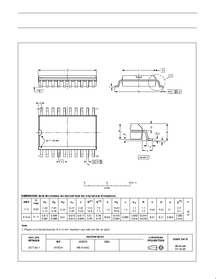
SO20:
plastic small outline package; 20 leads; body width 7.5 mm
SOT163-1

Philips Semiconductors
Product specification
74F524
8-bit register comparator (open-collector + 3-State)
1990 Aug 07
13
NOTES

Philips Semiconductors
Product specification
74F524
8-bit register comparator (open-collector + 3-State)
yyyy mmm dd
14
Definitions
Short-form specification -- The data in a short-form specification is extracted from a full data sheet with the same type number and title. For
detailed information see the relevant data sheet or data handbook.
Limiting values definition -- Limiting values given are in accordance with the Absolute Maximum Rating System (IEC 134). Stress above one
or more of the limiting values may cause permanent damage to the device. These are stress ratings only and operation of the device at these or
at any other conditions above those given in the Characteristics sections of the specification is not implied. Exposure to limiting values for extended
periods may affect device reliability.
Application information -- Applications that are described herein for any of these products are for illustrative purposes only. Philips
Semiconductors make no representation or warranty that such applications will be suitable for the specified use without further testing or
modification.
Disclaimers
Life support -- These products are not designed for use in life support appliances, devices or systems where malfunction of these products can
reasonably be expected to result in personal injury. Philips Semiconductors customers using or selling these products for use in such applications
do so at their own risk and agree to fully indemnify Philips Semiconductors for any damages resulting from such application.
Right to make changes -- Philips Semiconductors reserves the right to make changes, without notice, in the products, including circuits, standard
cells, and/or software, described or contained herein in order to improve design and/or performance. Philips Semiconductors assumes no
responsibility or liability for the use of any of these products, conveys no license or title under any patent, copyright, or mask work right to these
products, and makes no representations or warranties that these products are free from patent, copyright, or mask work right infringement, unless
otherwise specified.
Philips Semiconductors
811 East Arques Avenue
P.O. Box 3409
Sunnyvale, California 94088≠3409
Telephone 800-234-7381
©
Copyright Philips Electronics North America Corporation 1998
All rights reserved. Printed in U.S.A.
print code
Date of release: 10-98
Document order number:
9397-750-05131
Philips
Semiconductors
Data sheet
status
Objective
specification
Preliminary
specification
Product
specification
Product
status
Development
Qualification
Production
Definition
[1]
This data sheet contains the design target or goal specifications for product development.
Specification may change in any manner without notice.
This data sheet contains preliminary data, and supplementary data will be published at a later date.
Philips Semiconductors reserves the right to make chages at any time without notice in order to
improve design and supply the best possible product.
This data sheet contains final specifications. Philips Semiconductors reserves the right to make
changes at any time without notice in order to improve design and supply the best possible product.
Data sheet status
[1]
Please consult the most recently issued datasheet before initiating or completing a design.