 | –≠–ª–µ–∫—Ç—Ä–æ–Ω–Ω—ã–π –∫–æ–º–ø–æ–Ω–µ–Ω—Ç: N74F534D | –°–∫–∞—á–∞—Ç—å:  PDF PDF  ZIP ZIP |

Philips
Semiconductors
74F533*,74F534
Latch/flip-flop
Product specification
Supersedes data of 1989 May 11
IC15 Data Handbook
1999 Jan 08
INTEGRATED CIRCUITS
* Discontinued part. Please see the Discontinued Product List.
Philips Semiconductors
Product specification
74F533,* 74F534
Latch/flip-flop
74F533 Octal Transparent Latch, Inverting (3-State)
74F534 Octal D Flip-Flop, Inverting (3-State)
2
1999 Jan 08
853-0374 20616
* Discontinued part. Please see the Discontinued Products List.
FEATURES
∑
8-bit positive edge-triggered register ≠ 74F534
∑
3-State inverting output buffers
∑
Common 3-State Output register
∑
Independent register and 3-State buffer operation
DESCRIPTION
The 74F533 is an octal transparent latch coupled to eight 3-State
output buffers. The two sections of the device are controlled
independently by Enable (E) and Output Enable (OE) control gates.
The data on the D inputs is transferred to the latch outputs when the
Enable (E) input is High. The latch remains transparent to the data
input while E is High and stores the data that is present one setup
time before the High-to-Low enable transition.
The 3-State output buffers are designed to drive heavily loaded
3-State buses, MOS memories, or MOS microprocessors. The
active Low Output Enable (OE) controls all eight 3-State buffers
independent of the latch operation. When OE is Low, the latched or
transparent data appears at the outputs. When OE is High, the
outputs are in high impedance "off" state, which means they will
neither drive nor load the bus.
The 74F534 is an 8-bit edge-triggered register coupled to eight
3-State output buffers. The two sections of the device are controlled
independently by the Clock (CP) and Output Enable (OE) control
gates.
The register is fully edge-triggered. The state of each D input, one
setup time before the Low-to-High clock transition is transferred to
the corresponding flip-flop's Q output.
The 3-State output buffers are designed to drive heavily loaded
3-State buses, MOS memories, or MOS microprocessors. The
active Low Output Enable (OE) controls all eight 3-State buffers
independent of the latch operation. When OE is Low, the latched or
transparent data appears at the outputs. When OE is High, the
outputs are in high impedance "off" state, which means they will
neither drive nor load the bus.
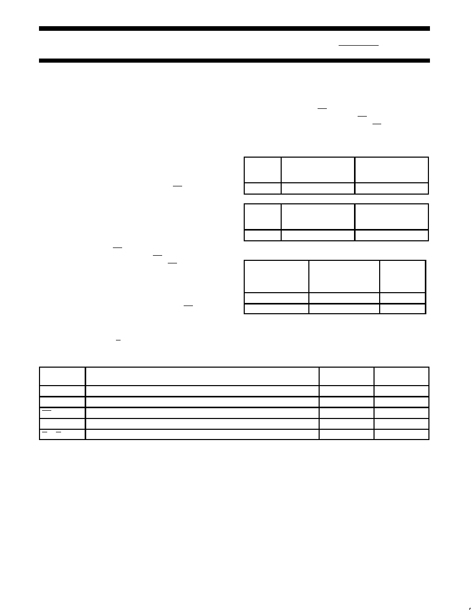
TYPE
TYPICAL
PROPAGATION DELAY
TYPICAL SUPPLY
CURRENT
(TOTAL)
74F533
5.5ns
41mA
TYPE
TYPICAL f
MAX
TYPICAL SUPPLY
CURRENT
(TOTAL)
74F534
165MHz
51mA
ORDERING INFORMATION
DESCRIPTION
COMMERCIAL
RANGE
V
CC
= 5V
±
10%,
T
amb
= 0
∞
C to +70
∞
C
PKG DWG #
20-Pin Plastic DIP
N74F534N
SOT146-1
20-Pin Plastic SOL
N74F534D
SOT163-1
INPUT AND OUTPUT LOADING AND FAN-OUT TABLE
PINS
DESCRIPTION
74F (U.L.)
HIGH/LOW
LOAD VALUE
HIGH/LOW
D0 - D7
Data inputs
1.0/1.0
20
µ
A/0.6mA
E (74F533)
Enable input (active High)
1.0/1.0
20
µ
A/0.6mA
OE
Output Enable input (active Low)
1.0/1.0
20
µ
A/0.6mA
CP (74F534)
Clock Pulse input (active rising edge)
1.0/1.0
20
µ
A/0.6mA
Q0 - Q7
Data outputs
150/40
3.0mA/24mA

Philips Semiconductors
Product specification
74F533,* 74F534
Latch/flip-flop
1999 Jan 08
3
* Discontinued part. Please see the Discontinued Products List.
NOTE: One (1.0) FAST Unit Load (U.L.) is defined as: 20
µ
A in the High state and 0.6mA in the Low state.
PIN CONFIGURATION ≠ 74F533
1
2
3
4
5
6
7
8
9
10
11
12
13
14
15
16
17
18
19
20
OE
Q0
D0
D1
Q1
Q2
D2
D3
Q3
Q4
GND
D4
D5
Q5
Q6
D6
D7
Q7
VCC
E
SF00981
PIN CONFIGURATION ≠ 74F534
1
2
3
4
5
6
7
8
9
10
11
12
13
14
15
16
17
18
19
20
OE
Q0
D0
D1
Q1
Q2
D2
D3
Q3
Q4
GND
D4
D5
Q5
Q6
D6
D7
Q7
VCC
CP
SF00982
LOGIC SYMBOL ≠ 74F533
3
4
7
8
13
14
15
12
9
6
5
2
1
11
E
OE
Q0
D0
D1
Q1
D2
Q2
Q3
D3
Q4
D4
Q5
D5
17
18
19
16
Q6
D6
Q7
D7
SF00983
V
CC
=Pin 20
GND=Pin 10
LOGIC SYMBOL (IEEE/IEC) ≠ 74F533
3
4
7
8
13
14
17
18
1
11
2D
2
5
6
9
12
15
16
19
EN1
EN2
1
SF00985
LOGIC SYMBOL ≠ 74F534
3
4
7
8
13
14
15
12
9
6
5
2
1
11
CP
OE
Q0
D0
D1
Q1
D2
Q2
Q3
D3
Q4
D4
Q5
D5
17
18
19
16
Q6
D6
Q7
D7
SF00984
V
CC
=Pin 20
GND=Pin 10
LOGIC SYMBOL (IEEE/IEC) ≠ 74F534
3
4
7
8
13
14
17
18
1
11
2D
2
5
6
9
12
15
16
19
EN1
C1
1
SF00986

Philips Semiconductors
Product specification
74F533,* 74F534
Latch/flip-flop
1999 Jan 08
4
* Discontinued part. Please see the Discontinued Products List.
LOGIC DIAGRAM ≠ 74F533
D0
D1
D2
D3
D4
D5
D6
D7
Q0
Q1
Q2
Q3
Q4
Q5
Q6
Q7
E
OE
3
4
7
8
13
14
17
18
19
16
15
12
9
6
5
2
1
11
E
D
Q
E
D
Q
E
Q
D
E
D
Q
E
D
Q
E
D
Q
E
D
Q
E
D
Q
V
CC
=Pin 20
GND=Pin 10
SF00987
LOGIC DIAGRAM ≠ 74F534
D0
D1
D2
D3
D4
D5
D6
D7
Q0
Q1
Q2
Q3
Q4
Q5
Q6
Q7
CP
OE
3
4
7
8
13
14
17
18
19
16
15
12
9
6
5
2
1
11
CP
D
Q
CP
D
Q
CP
Q
D
CP
D
Q
CP
D
Q
CP
D
Q
CP
D
Q
CP
D
Q
V
CC
=Pin 20
GND=Pin 10
SF00988
FUNCTION TABLE ≠ 74F533
INPUTS
INTERNAL
OUTPUTS
OPERATING MODES
OE
E
Dn
REGISTER
Q0 ≠ Q7
OPERATING MODES
L
L
H
H
L
H
L
H
H
L
Load and read register
L
L
l
h
L
H
H
L
Enable and read register
L
L
X
NC
NC
Hold
H
H
L
H
X
Dn
NC
Dn
Z
Z
Disable outputs
H = High voltage level
h = High voltage level one setup time prior to the High-to-Low E transition
L = Low voltage level
l
= Low voltage level one setup time prior to the High-to-Low E transition
NC= No change
X = Don't care
Z = High impedance "off" state
= High-to-Low E transition

Philips Semiconductors
Product specification
74F533,* 74F534
Latch/flip-flop
1999 Jan 08
5
* Discontinued part. Please see the Discontinued Products List.
FUNCTION TABLE ≠ 74F534
INPUTS
INTERNAL
OUTPUTS
OPERATING MODES
OE
CP
Dn
REGISTER
Q0 ≠ Q7
OPERATING MODES
L
L
l
h
L
H
H
L
Load and read register
L
X
NC
NC
Hold
H
H
X
Dn
NC
Dn
Z
Z
Disable outputs
H = High voltage level
h = High voltage level one setup time prior to the Low-to-High clock transition
L = Low voltage level
l
= Low voltage level one setup time prior to the Low-to-High clock transition
NC= No change
X = Don't care
Z = High impedance "off" state
= Low-to-High clock transition
= Not a Low-to-High clock transition
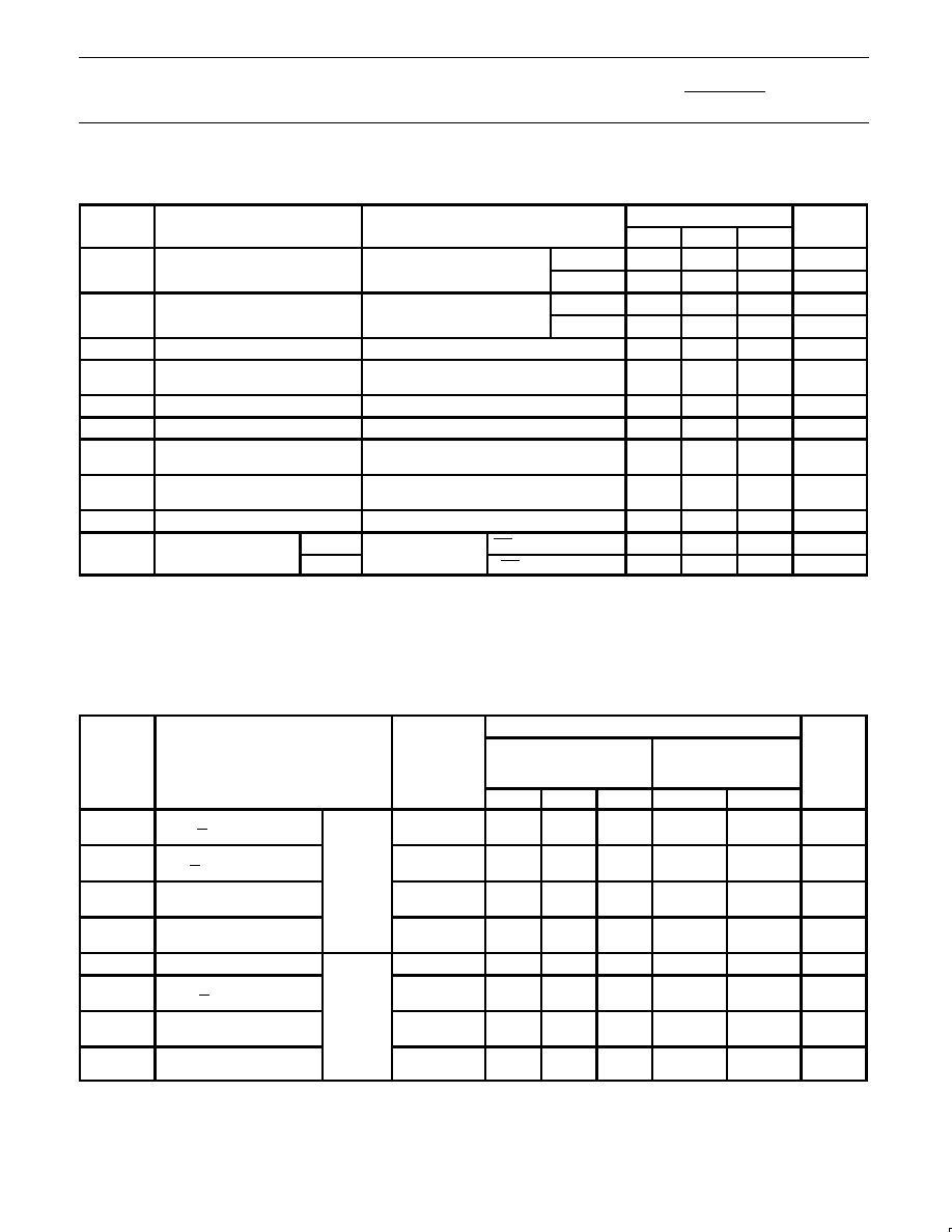
ABSOLUTE MAXIMUM RATINGS
(Operation beyond the limits set forth in this table may impair the useful life of the device.
Unless otherwise noted these limits are over the operating free-air temperature range.)
SYMBOL
PARAMETER
RATING
UNIT
V
CC
Supply voltage
≠0.5 to +7.0
V
V
IN
Input voltage
≠0.5 to +7.0
V
I
IN
Input current
≠30 to +5.0
mA
V
OUT
Voltage applied to output in High output state
≠0.5 to +V
CC
V
I
OUT
Current applied to output in Low output state
48
mA
T
amb
Operating free-air temperature range
0 to +70
∞
C
T
stg
Storage temperature
≠65 to +125
∞
C
RECOMMENDED OPERATING CONDITIONS
SYMBOL
PARAMETER
LIMITS
UNIT
SYMBOL
PARAMETER
MIN
NOM
MAX
UNIT
V
CC
Supply voltage
4.5
5.0
5.5
V
V
IH
High-level input voltage
2.0
V
V
IL
Low-level input voltage
0.8
V
I
IK
Input clamp current
≠18
mA
I
OH
High-level output current
≠3
mA
I
OL
Low-level output current
24
mA
T
amb
Operating free-air temperature range
0
70
∞
C
Philips Semiconductors
Product specification
74F533,* 74F534
Latch/flip-flop
1999 Jan 08
6
* Discontinued part. Please see the Discontinued Products List.
DC ELECTRICAL CHARACTERISTICS
(Over recommended operating free-air temperature range unless otherwise noted.)
SYMBOL
PARAMETER
TEST CONDITIONS
1
LIMITS
UNIT
SYMBOL
PARAMETER
TEST CONDITIONS
1
MIN
TYP
2
MAX
UNIT
V
O
High level output voltage
V
CC
= MIN, V
IL
= MAX,
±
10%V
CC
2.4
V
V
OH
High-level output voltage
V
CC
MIN, V
IL
MAX,
V
IH
= MIN, I
OH
= MAX
±
5%V
CC
2.7
3.3
V
V
O
Low level output voltage
V
CC
= MIN, V
IL
= MAX,
±
10%V
CC
0.35
0.50
V
V
OL
Low-level output voltage
V
CC
MIN, V
IL
MAX,
V
IH
= MIN, I
OL
= MAX
±
5%V
CC
0.35
0.50
V
V
IK
Input clamp voltage
V
CC
= MIN, I
I
= I
IK
≠0.73
≠1.2
V
I
I
Input current at
maximum input voltage
V
CC
= MAX, V
I
= 7.0V
100
µ
A
I
IH
High-level input current
V
CC
= MAX, V
I
= 2.7V
20
µ
A
I
IL
Low-level input current
V
CC
= MAX, V
I
= 0.5V
≠0.6
mA
I
OZH
Off-state output current,
High-level voltage applied
V
CC
= MAX, V
O
= 2.7V
50
µ
A
I
OZL
Off-state output current,
Low-level voltage applied
V
CC
= MAX, V
O
= 0.5V
≠50
µ
A
I
OS
Short-circuit output current
3
V
CC
= MAX
≠60
≠150
mA
I
CC
Supply current (total)
74F533
V
CC
= MAX
OE=4.5V, Dn=E=GND
41
61
mA
I
CC
Supply current (total)
74F534
V
CC
= MAX
OE=4.5V, Dn=GND
51
86
mA
NOTES:
1. For conditions shown as MIN or MAX, use the appropriate value specified under recommended operating conditions for the applicable type.
2. All typical values are at V
CC
= 5V, T
amb
= 25
∞
C.
3. Not more than one output should be shorted at a time. For testing I
OS
, the use of high-speed test apparatus and/or sample-and-hold
techniques are preferable in order to minimize internal heating and more accurately reflect operational values. Otherwise, prolonged shorting
of a High output may raise the chip temperature well above normal and thereby cause invalid readings in other parameter tests. In any
sequence of parameter tests, I
OS
tests should be performed last.
AC ELECTRICAL CHARACTERISTICS
LIMITS
SYMBOL
PARAMETER
TEST
CONDITIONS
T
amb
= +25
∞
C
V
CC
= +5V
C
L
= 50pF, R
L
= 500
T
amb
= 0
∞
C to +70
∞
C
V
CC
= +5V
±
10%
C
L
= 50pF, R
L
= 500
UNIT
MIN
TYP
MAX
MIN
MAX
t
PLH
t
PHL
Propagation delay
Dn to Qn
Waveform 2
4.0
3.0
6.0
4.5
8.5
7.0
4.0
3.0
9.5
8.0
ns
t
PLH
t
PHL
Propagation delay
E to Qn
74F533
Waveform 3
5.0
3.0
6.5
4.5
9.5
7.0
5.0
3.0
10.0
8.0
ns
t
PZH
t
PZL
Output Enable time
to High or Low level
74F533
Waveform 6
Waveform 7
2.0
2.0
4.5
5.0
7.0
7.0
2.0
2.0
8.0
8.0
ns
t
PHZ
t
PLZ
Output Disable time
from High or Low level
Waveform 6
Waveform 7
2.0
2.0
3.5
3.0
6.0
5.5
2.0
2.0
7.0
6.5
ns
f
MAX
Maximum Clock frequency
Waveform 1
150
165
135
MHz
t
PLH
t
PHL
Propagation delay
CP to Qn
Waveform 1
3.0
3.0
4.5
4.5
7.0
7.0
2.5
2.5
7.5
7.5
ns
t
PZH
t
PZL
Output Enable time
to High or Low level
74F534
Waveform 6
Waveform 7
2.0
2.0
4.5
5.0
7.5
7.5
2.0
2.0
8.5
8.5
ns
t
PHZ
t
PLZ
Output Disable time
from High or Low level
Waveform 6
Waveform 7
2.0
2.0
3.5
3.5
6.5
5.5
2.0
2.0
7.5
6.5
ns

Philips Semiconductors
Product specification
74F533,* 74F534
Latch/flip-flop
1999 Jan 08
7
* Discontinued part. Please see the Discontinued Products List.
AC SETUP REQUIREMENTS
LIMITS
SYMBOL
PARAMETER
TEST
CONDITIONS
T
amb
= +25
∞
C
V
CC
= +5V
C
L
= 50pF, R
L
= 500
T
amb
= 0
∞
C to +70
∞
C
V
CC
= +5.0V
±
10%
C
L
= 50pF, R
L
= 500
UNIT
MIN
TYP
MAX
MIN
MAX
t
s
(H)
t
s
(L)
Setup time,
Dn to E
Waveform 4
1.5
0
1.5
0
ns
t
h
(H)
t
h
(L)
Hold time,
Dn to E
74F533
Waveform 4
2.5
2.5
2.5
2.5
ns
t
w
(H)
E Pulse width,
High
Waveform 3
3.0
3.0
ns
t
s
(H)
t
s
(L)
Setup time,
Dn to CP
Waveform 5
2.0
2.0
2.5
2.5
ns
t
h
(H)
t
h
(L)
Hold time,
Dn to CP
74F534
Waveform 5
0
0
0
0
ns
t
w
(H)
t
w
(L)
CP pulse width,
High or Low
Waveform 1
3.0
3.5
3.5
4.0
ns
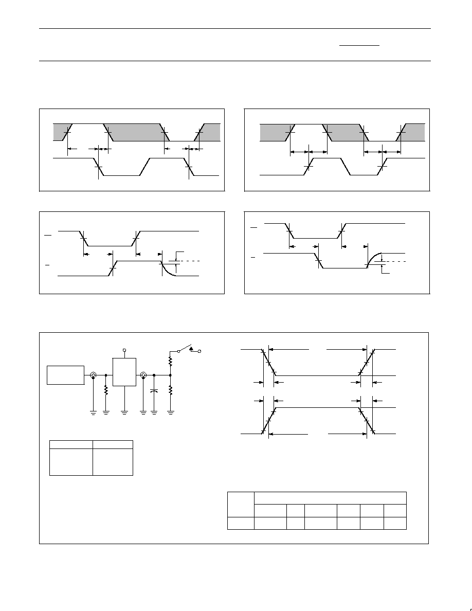
AC WAVEFORMS
For all waveforms, V
M
= 1.5V
The shaded areas indicate when the input is permitted to change for predictable output performance.
tW(H)
CP
Qn
VM
VM
VM
VM
VM
1/fMAX
tW(L)
tPLH
tPHL
SF00989
Waveform 1. Propagation Delay, Clock and Enable Inputs
to Output, Enable, Clock Pulse Widths,
and Maximum Clock Frequency
VM
VM
VM
tPHL
Dn
Qn
VM
tPLH
SF00990
Waveform 2. Propagation Delay for Data to Output
tW(H)
E
Qn
VM
VM
VM
VM
VM
tW(L)
tPLH
tPHL
Dn
SF00991
Waveform 3. Propagation Delay, Enable Input to Output,
and Enable Pulse Width
Philips Semiconductors
Product specification
74F533,* 74F534
Latch/flip-flop
1999 Jan 08
8
* Discontinued part. Please see the Discontinued Products List.
AC WAVEFORMS (Continued)
For all waveforms, V
M
= 1.5V
The shaded areas indicate when the input is permitted to change for predictable output performance.
E
Dn
VM
VM
VM
VM
VM
VM
ts(L)
ts(H)
th(L)
th(H)
SF00992
Waveform 4. Data Setup and Hold Times
th(H)
ts(H)
CP
SF00191
VM
VM
VM
VM
VM
VM
th(L)
ts(L)
Dn
Waveform 5. Data Setup and Hold Times
VM
VM
VM
tPHZ
tPZH
OE
Qn
VOH -0.3V
0V
SF00994
Waveform 6. 3-State Output Enable Time to High Level
and Output Disable Time from High Level
VM
VM
VM
tPLZ
tPZL
OE
Qn
VOL +0.3V
SF00995
Waveform 7. 3-State Output Enable Time to Low Level
and Output Disable Time from Low Level
TEST CIRCUIT AND WAVEFORM
tw
90%
VM
10%
90%
VM
10%
90%
VM
10%
90%
VM
10%
NEGATIVE
PULSE
POSITIVE
PULSE
tw
AMP (V)
0V
0V
tTHL (tf
)
INPUT PULSE REQUIREMENTS
rep. rate
t
w
t
TLH
t
THL
1MHz
500ns
2.5ns
2.5ns
Input Pulse Definition
VCC
family
74F
D.U.T.
PULSE
GENERATOR
RL
CL
RT
VIN
VOUT
Test Circuit for 3-State Outputs
DEFINITIONS:
R
L
= Load resistor;
see AC electrical characteristics for value.
C
L
= Load capacitance includes jig and probe capacitance;
see AC electrical characteristics for value.
R
T
= Termination resistance should be equal to Z
OUT
of
pulse generators.
tTHL (tf
)
tTLH (tr
)
tTLH (tr
)
AMP (V)
amplitude
3.0V
1.5V
V
M
RL
7.0V
SF00777
TEST
SWITCH
t
PLZ
closed
t
PZL
closed
All other
open
SWITCH POSITION
Philips Semiconductors
Product specification
74F533*, 74F534
Latch/flip-flop
1999 Jan 08
9
* Discontinued part. Please see the Discontinued Product List.
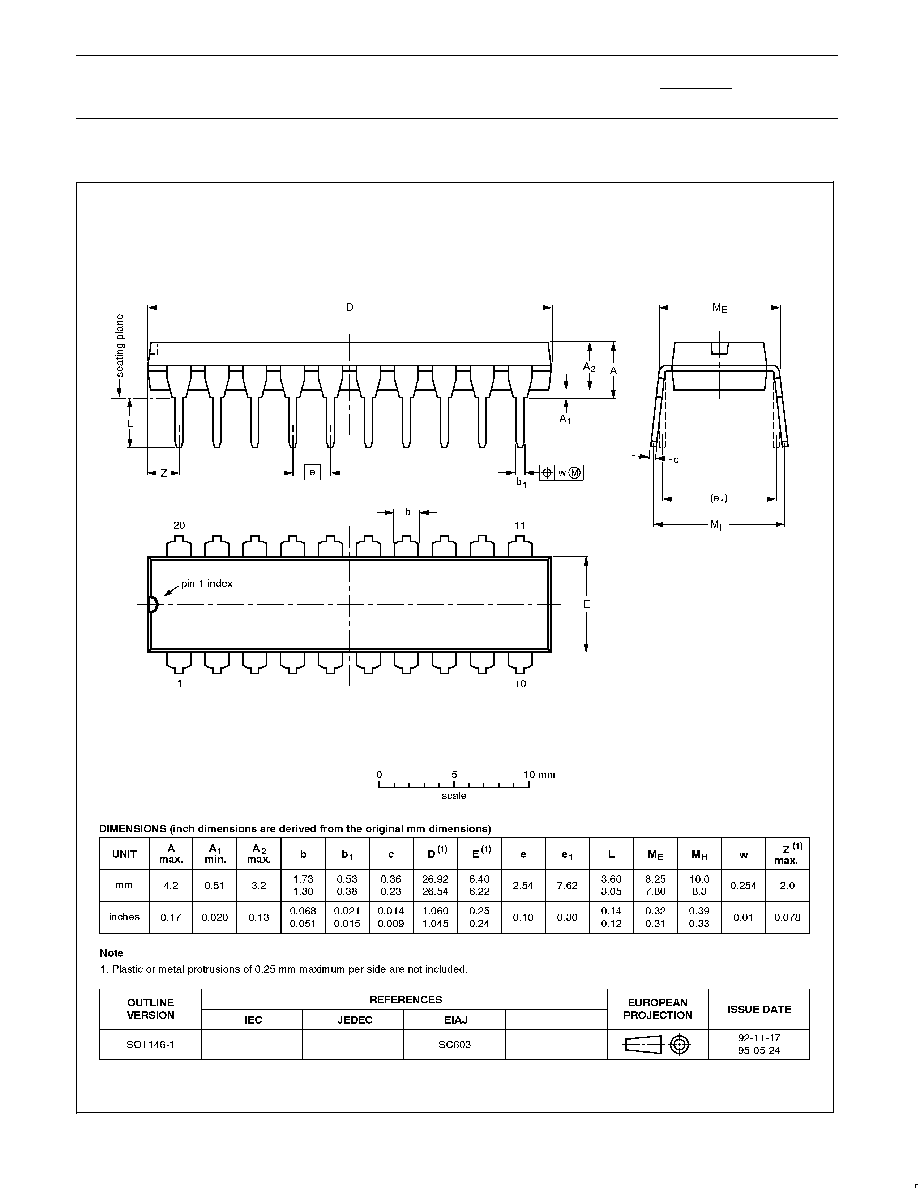
DIP20:
plastic dual in-line package; 20 leads (300 mil)
SOT146-1
Philips Semiconductors
Product specification
74F533*, 74F534
Latch/flip-flop
1999 Jan 08
10
* Discontinued part. Please see the Discontinued Product List.
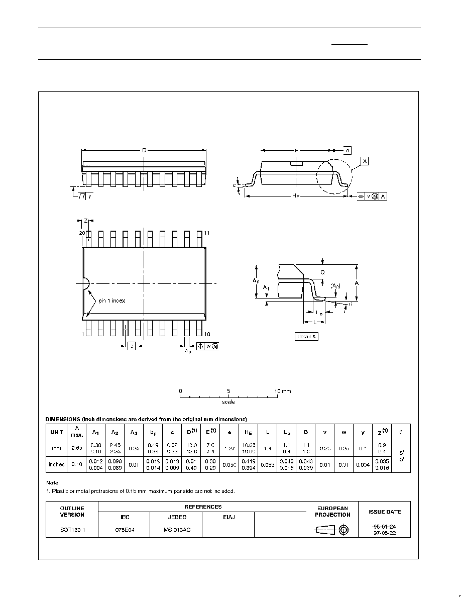
SO20:
plastic small outline package; 20 leads; body width 7.5 mm
SOT163-1

Philips Semiconductors
Product specification
74F533*, 74F534
Latch/flip-flop
1999 Jan 08
11
* Discontinued part. Please see the Discontinued Product List.
NOTES
Philips Semiconductors
Product specification
74F533*, 74F534
Latch/flip-flop
yyyy mmm dd
12
Definitions
Short-form specification -- The data in a short-form specification is extracted from a full data sheet with the same type number and title. For
detailed information see the relevant data sheet or data handbook.
Limiting values definition -- Limiting values given are in accordance with the Absolute Maximum Rating System (IEC 134). Stress above one
or more of the limiting values may cause permanent damage to the device. These are stress ratings only and operation of the device at these or
at any other conditions above those given in the Characteristics sections of the specification is not implied. Exposure to limiting values for extended
periods may affect device reliability.
Application information -- Applications that are described herein for any of these products are for illustrative purposes only. Philips
Semiconductors make no representation or warranty that such applications will be suitable for the specified use without further testing or
modification.
Disclaimers
Life support -- These products are not designed for use in life support appliances, devices or systems where malfunction of these products can
reasonably be expected to result in personal injury. Philips Semiconductors customers using or selling these products for use in such applications
do so at their own risk and agree to fully indemnify Philips Semiconductors for any damages resulting from such application.
Right to make changes -- Philips Semiconductors reserves the right to make changes, without notice, in the products, including circuits, standard
cells, and/or software, described or contained herein in order to improve design and/or performance. Philips Semiconductors assumes no
responsibility or liability for the use of any of these products, conveys no license or title under any patent, copyright, or mask work right to these
products, and makes no representations or warranties that these products are free from patent, copyright, or mask work right infringement, unless
otherwise specified.
Philips Semiconductors
811 East Arques Avenue
P.O. Box 3409
Sunnyvale, California 94088≠3409
Telephone 800-234-7381
©
Copyright Philips Electronics North America Corporation 1998
All rights reserved. Printed in U.S.A.
print code
Date of release: 10-98
Document order number:
9397-750-05132
Philips
Semiconductors
Data sheet
status
Objective
specification
Preliminary
specification
Product
specification
Product
status
Development
Qualification
Production
Definition
[1]
This data sheet contains the design target or goal specifications for product development.
Specification may change in any manner without notice.
This data sheet contains preliminary data, and supplementary data will be published at a later date.
Philips Semiconductors reserves the right to make chages at any time without notice in order to
improve design and supply the best possible product.
This data sheet contains final specifications. Philips Semiconductors reserves the right to make
changes at any time without notice in order to improve design and supply the best possible product.
Data sheet status
[1]
Please consult the most recently issued datasheet before initiating or completing a design.
* Discontinued part. Please see the Discontinued Product List.