 | –≠–ª–µ–∫—Ç—Ä–æ–Ω–Ω—ã–π –∫–æ–º–ø–æ–Ω–µ–Ω—Ç: N74F540D | –°–∫–∞—á–∞—Ç—å:  PDF PDF  ZIP ZIP |

Philips
Semiconductors
74F540
Octal inverter buffer (3- State)
74F541
Octal buffer (3- State)
Product specification
IC15 Data Handbook
1990 Jan 08
INTEGRATED CIRCUITS
Philips Semiconductors
Product specification
74F540, 74F541
Buffers
74F540 Octal Inverter Buffer (3-State)
74F541 Octal Buffer (3-State)
2
1990 Jan 08
853≠0068 98494
FEATURES
∑
High impedance NPN base inputs for reduced loading
(20
µ
A in High and Low states)
∑
Low power, light bus loading
∑
Functionally similar to the 74F240 and 74F241
∑
Provides ideal interface and increases fan-out of MOS
microprocessors
∑
Efficient pinout to facilitate PC board layout
∑
Octal bus interface
∑
3-State buffer outputs sink 64mA
∑
15mA source current
DESCRIPTION
The 74F540 and 74F541 are octal buffers that are ideal for driving
bus lines or buffer memory address registers. The outputs are
capable of sinking 64mA and sourcing up to 15mA, producing very
good capacitive drive characteristics. The devices feature input and
outputs on opposite sides of the package to facilitate printed circuit
board layout.
TYPE
TYPICAL
PROPAGATION DELAY
TYPICAL SUPPLY
CURRENT
(TOTAL)
74F540
3.5ns
58mA
74F541
5.5ns
55mA
ORDERING INFORMATION
DESCRIPTION
COMMERCIAL RANGE
V
CC
= 5V
±
10%,
T
amb
= 0
∞
C to +70
∞
C
PKG DWG #
20-Pin Plastic DIP
N74F540, N74F541N
SOT146-1
20-Pin Plastic SOL
N74F540D, N74F541D
SOT163-1
INPUT AND OUTPUT LOADING AND FAN-OUT TABLE
PINS
DESCRIPTION
74F(U.L.)
HIGH/LOW
LOAD VALUE
HIGH/LOW
I0≠I7
Data inputs
1.0/0.033
20
µ
A/20
µ
A
OE0, OE1
3-State output enable inputs (active Low)
1.0/0.033
20
µ
A/20
µ
A
Y0 - Y7
Data outputs (74F541)
750/106.7
15mA/64mA
Y0 - Y7
Data outputs (74F540)
750/106.7
15mA/64mA
NOTE: One (1.0) FAST Unit Load is defined as: 20
µ
A in the High state and 0.6mA in the Low state.
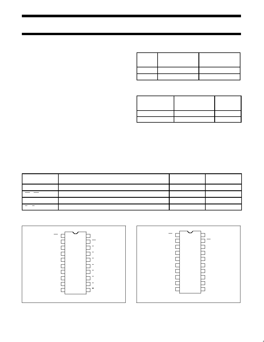
PIN CONFIGURATION ≠ 74F540
20
19
18
17
16
15
14
13
12
10
11
9
8
7
6
5
4
3
2
1
V
CC
OE1
Y0
Y1
Y4
Y5
Y6
Y7
OE0
I0
I1
I4
I5
I6
I7
GND
Y2
Y3
I3
I2
SF01060
PIN CONFIGURATION ≠ 74F541
20
19
18
17
16
15
14
13
12
10
11
9
8
7
6
5
4
3
2
1
V
CC
OE1
Y0
Y1
Y4
Y5
Y6
Y7
OE0
I0
I1
I4
I5
I6
I7
GND
Y2
Y3
I3
I2
SF01021
Philips Semiconductors
Product specification
74F540, 74F541
Buffers
1990 Jan 08
3
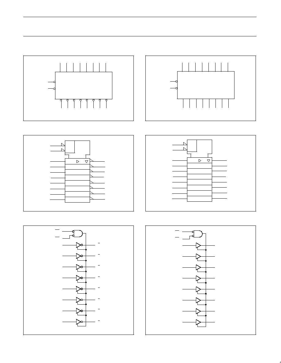
LOGIC SYMBOL ≠ 74F540
2
3
4
V
CC
= Pin 20
GND = Pin 10
18
17
16
15
14
13
12
11
1
19
SF01022
OE1
Y0
Y1
Y4
Y5
Y6
Y7
OE0
I0
I1
I4
I5
I6
I7
Y2
Y3
I3
I2
5
6
7
8
9
LOGIC SYMBOL ≠ 74F541
2
3
4
V
CC
= Pin 20
GND = Pin 10
18
17
16
15
14
13
12
11
1
19
SF01023
OE1
Y0
Y1
Y4
Y5
Y6
Y7
OE0
I0
I1
I4
I5
I6
I7
Y2
Y3
I3
I2
5
6
7
8
9
LOGIC SYMBOL (IEEE/IEC) ≠ 74F540
2
3
4
5
6
7
8
9
1
19
18
17
16
15
14
13
12
11
EN
SF01024
&
LOGIC SYMBOL (IEEE/IEC) ≠ 74F541
2
3
4
5
6
7
8
9
1
19
18
17
16
15
14
13
12
11
EN
SF01025
&
LOGIC DIAGRAM ≠ 74F540
VCC =
Pin 20
GND =
Pin 10
SF01026
11
12
13
14
15
16
17
18
OE0
OE1
Y0
Y1
Y4
Y5
Y6
Y7
I0
I1
I4
I5
I6
I7
Y2
Y3
I3
I2
1
19
2
3
4
5
6
7
8
9
LOGIC DIAGRAM ≠ 74F541
VCC =
Pin 20
GND =
Pin 10
SF01027
Y0
Y1
Y2
Y3
Y4
Y5
Y6
Y7
11
12
13
14
15
16
17
18
OE0
OE1
I0
I1
I4
I5
I6
I7
I3
I2
1
19
2
3
4
5
6
7
8
9

Philips Semiconductors
Product specification
74F540, 74F541
Buffers
1990 Jan 08
4
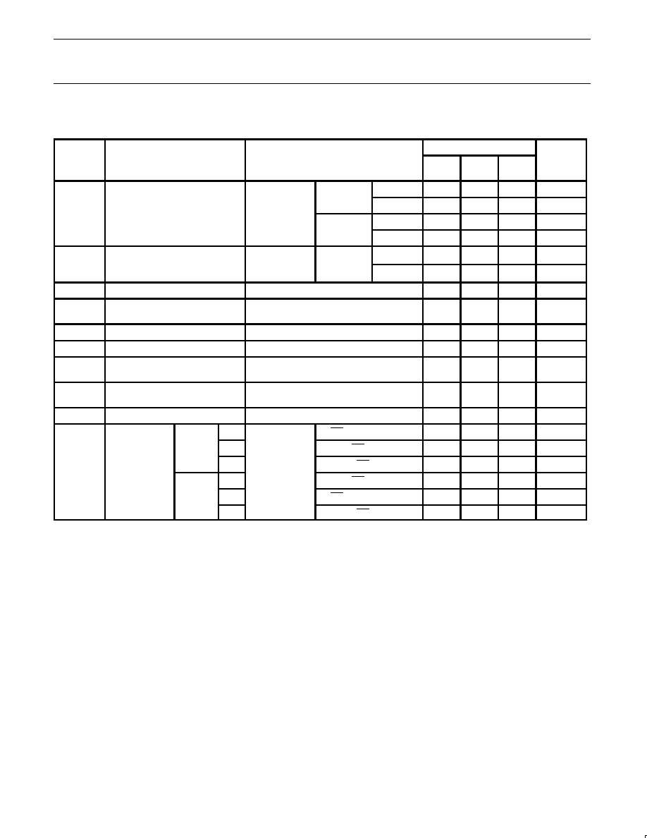
FUNCTION TABLE
INPUTS
OUTPUTS
INPUTS
74F541
74F540
OE0
OE1
In
Yn
Yn
L
L
X
H
L
L
H
X
L
H
X
X
L
H
Z
Z
H
L
Z
Z
H = High voltage level
L = Low voltage level
X = Don't care
Z = High impedance "off" state
ABSOLUTE MAXIMUM RATINGS
(Operation beyond the limits set forth in this table may impair the useful life of the device.
Unless otherwise noted these limits are over the operating free-air temperature range.)
SYMBOL
PARAMETER
RATING
UNIT
V
CC
Supply voltage
≠0.5 to +7.0
V
V
IN
Input voltage
≠0.5 to +7.0
V
I
IN
Input current
≠30 to +5.0
mA
V
OUT
Voltage applied to output in High output state
≠0.5 to +V
CC
V
I
OUT
Current applied to output in Low output state
128
mA
T
amb
Operating free-air temperature range
0 to +70
∞
C
T
stg
Storage temperature
≠65 to +150
∞
C
RECOMMENDED OPERATING CONDITIONS
SYMBOL
PARAMETER
LIMITS
UNIT
SYMBOL
PARAMETER
MIN
NOM
MAX
UNIT
V
CC
Supply voltage
4.5
5.0
5.5
V
V
IH
High-level input voltage
2.0
V
V
IL
Low-level input voltage
0.8
V
I
IK
Input clamp current
≠18
mA
I
OH
High-level output current
≠15
mA
I
OL
Low-level output current
64
mA
T
amb
Operating free-air temperature range
0
70
∞
C
Philips Semiconductors
Product specification
74F540, 74F541
Buffers
1990 Jan 08
5
DC ELECTRICAL CHARACTERISTICS
(Over recommended operating free-air temperature range unless otherwise noted.)
NO TAG
LIMITS
SYMBOL
PARAMETER
TEST CONDITIONS
NO TAG
MIN
TYP
NO TAG
MAX
UNIT
I
O
= 3mA
±
10%V
CC
2.4
V
V
O
High level output voltage
V
CC
= MIN,
V
IL
= MAX
I
OH
= ≠3mA
±
5%V
CC
2.7
3.4
V
V
OH
High-level output voltage
V
IL
= MAX,
V
IH
= MIN
I
O
= 15mA
±
10%V
CC
2.0
V
I
OH
= ≠15mA
±
5%V
CC
2.0
V
V
O
Low level output voltage
V
CC
= MIN,
V
IL
= MAX
I
O
= MAX
±
10%V
CC
0.55
V
V
OL
Low-level output voltage
V
IL
= MAX,
V
IH
= MIN
I
OL
= MAX
±
5%V
CC
0.42
0.55
V
V
IK
Input clamp voltage
V
CC
= MIN, I
I
= I
IK
≠0.73
≠1.2
V
I
I
Input current at maximum input
voltage
V
CC
= 0.0V, V
I
= 7.0V
100
µ
A
I
IH
High-level input current
V
CC
= MAX, V
I
= 2.7V
20
µ
A
I
IL
Low-level input current
V
CC
= MAX, V
I
= 0.5V
≠20
µ
A
I
OZH
Off-state output current
High-level voltage applied
V
CC
= MAX, V
O
= 2.7V
50
µ
A
I
OZL
Off-state output current
Low-level voltage applied
V
CC
= MAX, V
O
= 0.5V
≠50
µ
A
I
OS
Short-circuit output current
NO TAG
V
CC
= MAX
≠100
≠225
mA
I
CCH
In=OEn=GND
22
30
mA
74F540
I
CCL
In=4.5V, OEn=GND
58
75
mA
I
CC
Supply current
I
CCZ
V
CC
= MAX
In=GND, OEn=4.5V
40
55
mA
I
CC
y
(total)
I
CCH
V
CC
= MAX
In=4.5V, OEn=GND
30
40
mA
74F541
I
CCL
In=OEn=GND
55
72
mA
I
CCZ
In=GND, OEn=4.5V
45
58
mA
NOTES:
1. For conditions shown as MIN or MAX, use the appropriate value under the recommended operating conditions for the applicable type.
2. All typical values are at V
CC
= 5V, T
amb
= 25
∞
C.
3. Not more than one output should be shorted at a time. For testing I
OS
, the use of high-speed test apparatus and/or sample-and-hold
techniques are preferable in order to minimize internal heating and more accurately reflect operational values. Otherwise, prolonged shorting
of a High output may raise the chip temperature well above normal and thereby cause invalid readings in other parameter tests. In any
sequence of parameter tests, I
OS
should be performed last.
Philips Semiconductors
Product specification
74F540, 74F541
Buffers
1990 Jan 08
6
AC ELECTRICAL CHARACTERISTICS
LIMITS
TEST
T
amb
= +25
∞
C
T
amb
= 0
∞
C to +70
∞
C
SYMBOL
PARAMETER
TEST
CONDITIONS
V
CC
= +5.0V
V
CC
= +5.0V
±
10%
UNIT
CONDITIONS
C
L
= 50pF, R
L
= 500
C
L
= 50pF, R
L
= 500
MIN
TYP
MAX
MIN
MAX
t
PLH
t
PHL
Propagation delay
In to Yn
Waveform 1
3.0
1.5
4.5
2.5
6.5
4.5
2.5
1.5
7.5
5.0
ns
ns
t
PZH
t
PZL
Output Enable time
to High or Low level
74F540
Waveform 3
Waveform 4
2.0
4.0
3.5
7.5
6.5
9.5
2.0
4.0
7.0
10.0
ns
ns
t
PZH
t
PZL
Output Disable time
from High or Low level
Waveform 3
Waveform 4
2.0
2.0
4.0
4.0
6.0
5.5
2.0
2.0
6.5
6.0
ns
ns
t
PLH
t
PHL
Propagation delay
In to Yn
Waveform 2
2.5
3.5
5.0
6.0
6.5
7.0
2.5
3.0
7.0
7.5
ns
ns
t
PZH
t
PZL
Output Enable time
to High or Low level
74F541
Waveform 3
Waveform 4
3.0
3.0
5.5
6.5
7.0
8.5
3.0
3.0
7.5
9.5
ns
ns
t
PZH
t
PZL
Output Disable time
from High or Low level
Waveform 3
Waveform 4
2.0
2.0
4.0
4.0
7.0
7.0
2.0
2.0
7.5
7.5
ns
ns
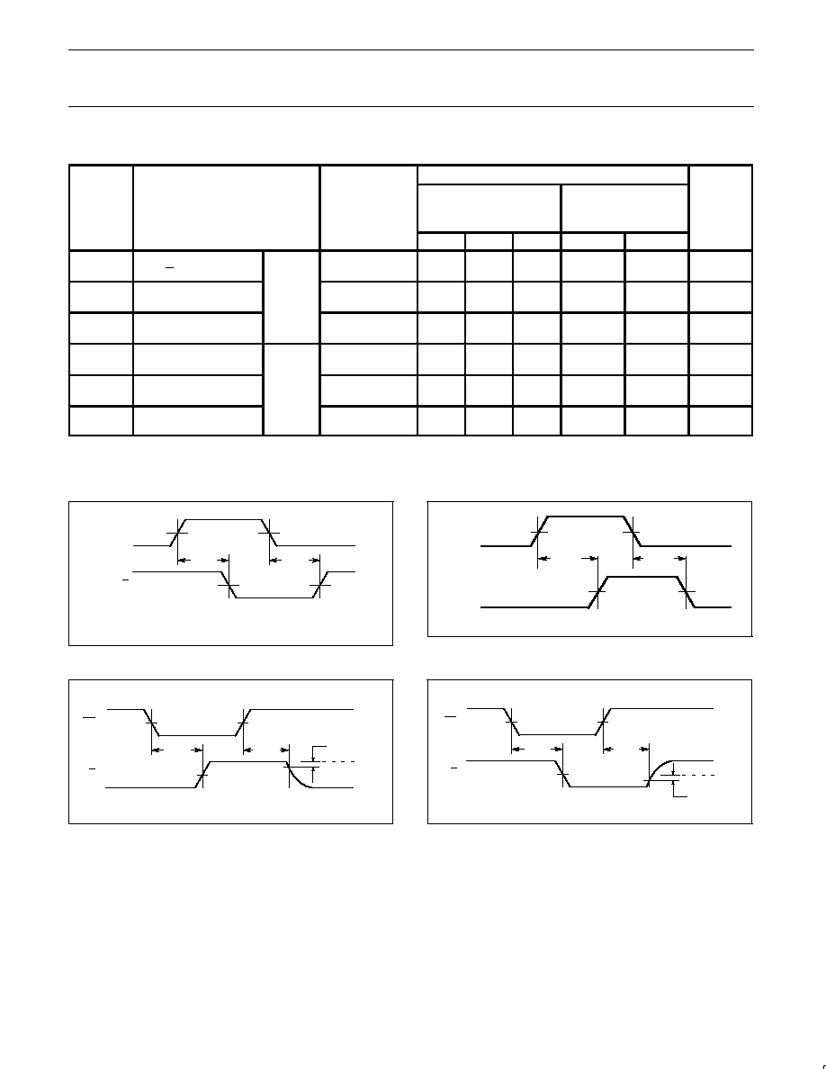
AC WAVEFORMS
For all waveforms, V
M
= 1.5V.
V
M
V
M
V
M
V
M
t
PLH
t
PHL
In
Yn
SF01028
Waveform 1. Propagation Delay Data to Outputs for 74F540
VM
VM
VM
VM
Yn
In
tPLH
tPHL
SF00150
Waveform 2. Propagation Delay Data to Outputs for 74F541
V
M
V
M
V
M
t
PHZ
t
PZH
OEn
Yn, Yn
V
OH
-0.3V
0V
SF01030
Waveform 3. 3-State Output Enable Time to High Level
and Output Disable Time from High Level
V
M
V
M
V
M
t
PLZ
t
PZL
OEn
Yn, Yn
V
OL
+0.3V
SF01031
Waveform 4. 3-State Output Enable Time to Low Level
and Output Disable Time from Low Level
Philips Semiconductors
Product specification
74F540, 74F541
Buffers
1990 Jan 08
7
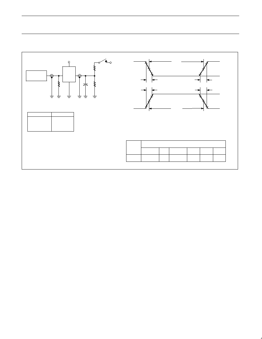
TEST CIRCUIT AND WAVEFORM
tw
90%
VM
10%
90%
VM
10%
90%
VM
10%
90%
VM
10%
NEGATIVE
PULSE
POSITIVE
PULSE
tw
AMP (V)
0V
0V
tTHL (tf
)
INPUT PULSE REQUIREMENTS
rep. rate
t
w
t
TLH
t
THL
1MHz
500ns
2.5ns
2.5ns
Input Pulse Definition
VCC
family
74F
D.U.T.
PULSE
GENERATOR
RL
CL
RT
VIN
VOUT
Test Circuit for 3-State Outputs
DEFINITIONS:
R
L
= Load resistor;
see AC electrical characteristics for value.
C
L
= Load capacitance includes jig and probe capacitance;
see AC electrical characteristics for value.
R
T
= Termination resistance should be equal to Z
OUT
of
pulse generators.
tTHL (tf
)
tTLH (tr
)
tTLH (tr
)
AMP (V)
amplitude
3.0V
1.5V
V
M
RL
7.0V
SF00777
TEST
SWITCH
t
PLZ
closed
t
PZL
closed
All other
open
SWITCH POSITION
Philips Semiconductors
Product specification
74F540, 74F541
Buffers
1990 Jan 08
8
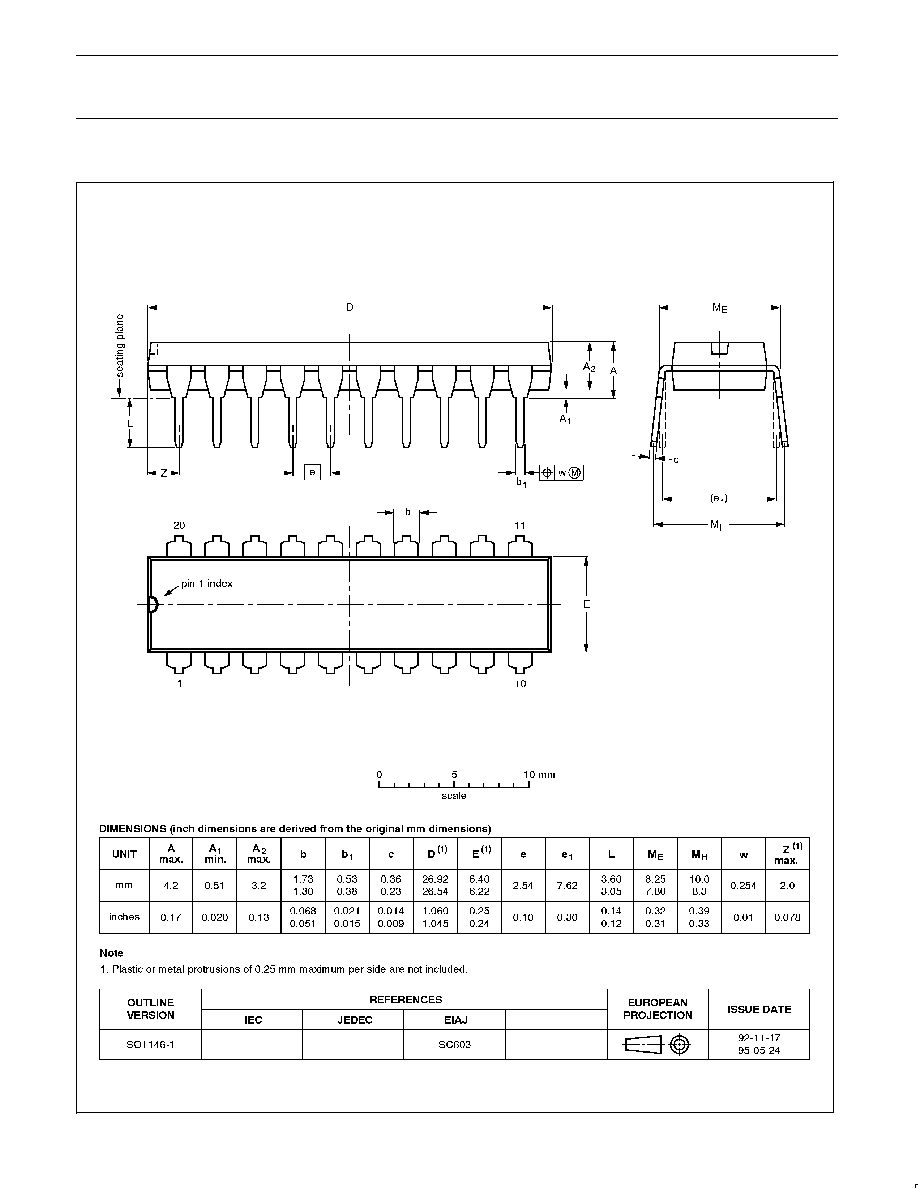
DIP20:
plastic dual in-line package; 20 leads (300 mil)
SOT146-1
Philips Semiconductors
Product specification
74F540, 74F541
Buffers
1990 Jan 08
9
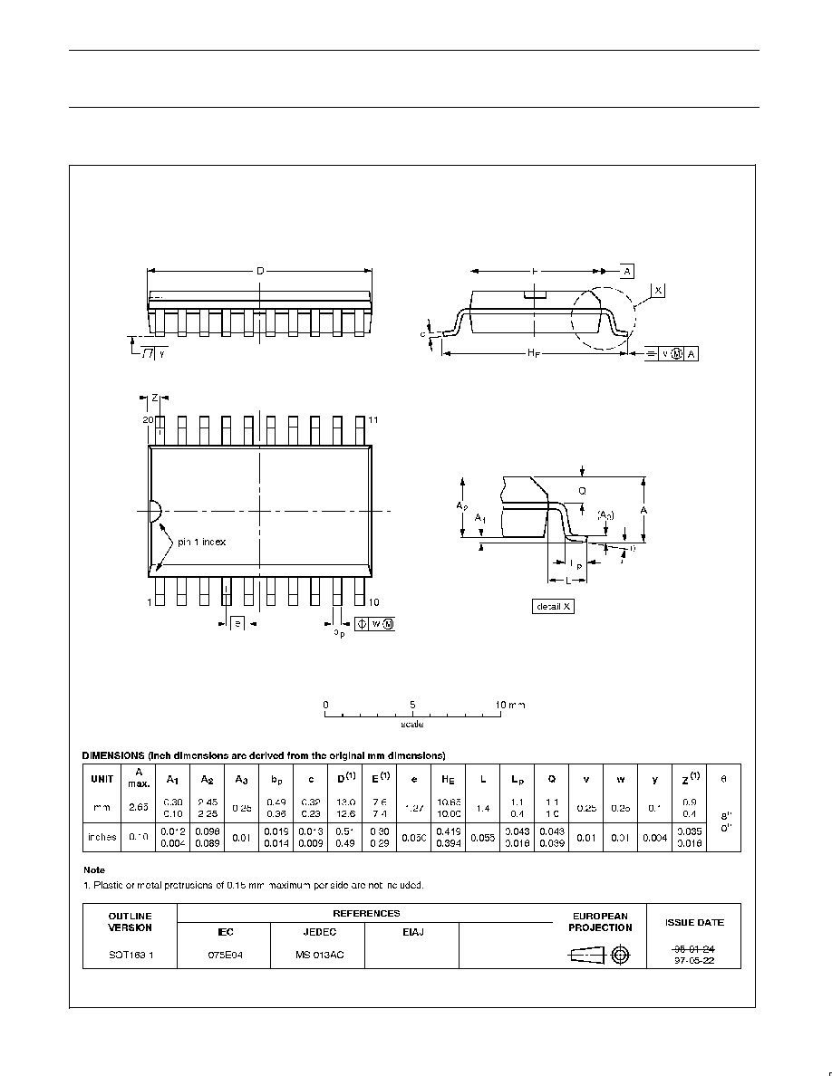
SO20:
plastic small outline package; 20 leads; body width 7.5 mm
SOT163-1
Philips Semiconductors
Product specification
74F540, 74F541
Buffers
yyyy mmm dd
10
Definitions
Short-form specification -- The data in a short-form specification is extracted from a full data sheet with the same type number and title. For
detailed information see the relevant data sheet or data handbook.
Limiting values definition -- Limiting values given are in accordance with the Absolute Maximum Rating System (IEC 134). Stress above one
or more of the limiting values may cause permanent damage to the device. These are stress ratings only and operation of the device at these or
at any other conditions above those given in the Characteristics sections of the specification is not implied. Exposure to limiting values for extended
periods may affect device reliability.
Application information -- Applications that are described herein for any of these products are for illustrative purposes only. Philips
Semiconductors make no representation or warranty that such applications will be suitable for the specified use without further testing or
modification.
Disclaimers
Life support -- These products are not designed for use in life support appliances, devices or systems where malfunction of these products can
reasonably be expected to result in personal injury. Philips Semiconductors customers using or selling these products for use in such applications
do so at their own risk and agree to fully indemnify Philips Semiconductors for any damages resulting from such application.
Right to make changes -- Philips Semiconductors reserves the right to make changes, without notice, in the products, including circuits, standard
cells, and/or software, described or contained herein in order to improve design and/or performance. Philips Semiconductors assumes no
responsibility or liability for the use of any of these products, conveys no license or title under any patent, copyright, or mask work right to these
products, and makes no representations or warranties that these products are free from patent, copyright, or mask work right infringement, unless
otherwise specified.
Philips Semiconductors
811 East Arques Avenue
P.O. Box 3409
Sunnyvale, California 94088≠3409
Telephone 800-234-7381
©
Copyright Philips Electronics North America Corporation 1998
All rights reserved. Printed in U.S.A.
print code
Date of release: 10-98
Document order number:
9397-750-05134
Philips
Semiconductors
Data sheet
status
Objective
specification
Preliminary
specification
Product
specification
Product
status
Development
Qualification
Production
Definition
[1]
This data sheet contains the design target or goal specifications for product development.
Specification may change in any manner without notice.
This data sheet contains preliminary data, and supplementary data will be published at a later date.
Philips Semiconductors reserves the right to make chages at any time without notice in order to
improve design and supply the best possible product.
This data sheet contains final specifications. Philips Semiconductors reserves the right to make
changes at any time without notice in order to improve design and supply the best possible product.
Data sheet status
[1]
Please consult the most recently issued datasheet before initiating or completing a design.