 | –≠–ª–µ–∫—Ç—Ä–æ–Ω–Ω—ã–π –∫–æ–º–ø–æ–Ω–µ–Ω—Ç: N74F552N | –°–∫–∞—á–∞—Ç—å:  PDF PDF  ZIP ZIP |

Philips
Semiconductors
74F552
Octal registered transceiver with parity
and flags (3-State)
Product specification
IC15 Data Handbook
1991 Jan 02
INTEGRATED CIRCUITS
Philips Semiconductors
Product specification
74F552
Octal registered transceiver with parity and flags (3-State)
2
1991 Jan 02
853≠1098 01347
FEATURES
∑
8-bit bidirectional I/O port with handshake
∑
Register status flag flip-flops
∑
Separate clock enable and output enable
∑
Parity generation and parity check
∑
B outputs and parity output sink 64mA
DESCRIPTION
The 74F522 Octal Registered Transceiver contains two 8-bit
registers for temporary storage of data flowing in either direction.
Each register has its own clock (CPR, CPS) and Clock Enable
(CER, CES) inputs, as well as a flag flip-flop that is set automatically
as the register is loaded. The flag output will be reset when the
Output Enable returns to High after reading the output port. Each
register has a separate Output Enable (OEAS, OEBR) for its 3-State
buffer. The separate Clocks, Flags and Enables provide
considerable flexibility as I/O ports for demand-response data
transfer. When data is transferred from the A port to the B port, a
parity bit is generated. On the other hand, when data is transferred
from the B port to the A port, the parity of input data on B0≠B7 is
checked.
TYPE
TYPICAL f
MAX
TYPICAL SUPPLY
CURRENT
(TOTAL)
74F552
85MHz
120mA
ORDERING INFORMATION
DESCRIPTION
COMMERCIAL RANGE
V
CC
= 5V
±
10%,
T
amb
= 0
∞
C to +70
∞
C
PKG DWG #
28-Pin Plastic DIP
(600mil)
N74F552N
SOT117-2
28-Pin Plastic SOL
N74F552D
SOT136-1
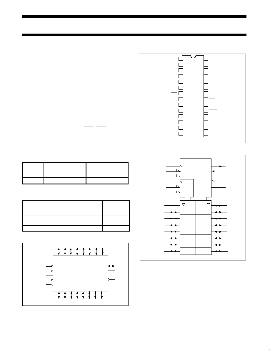
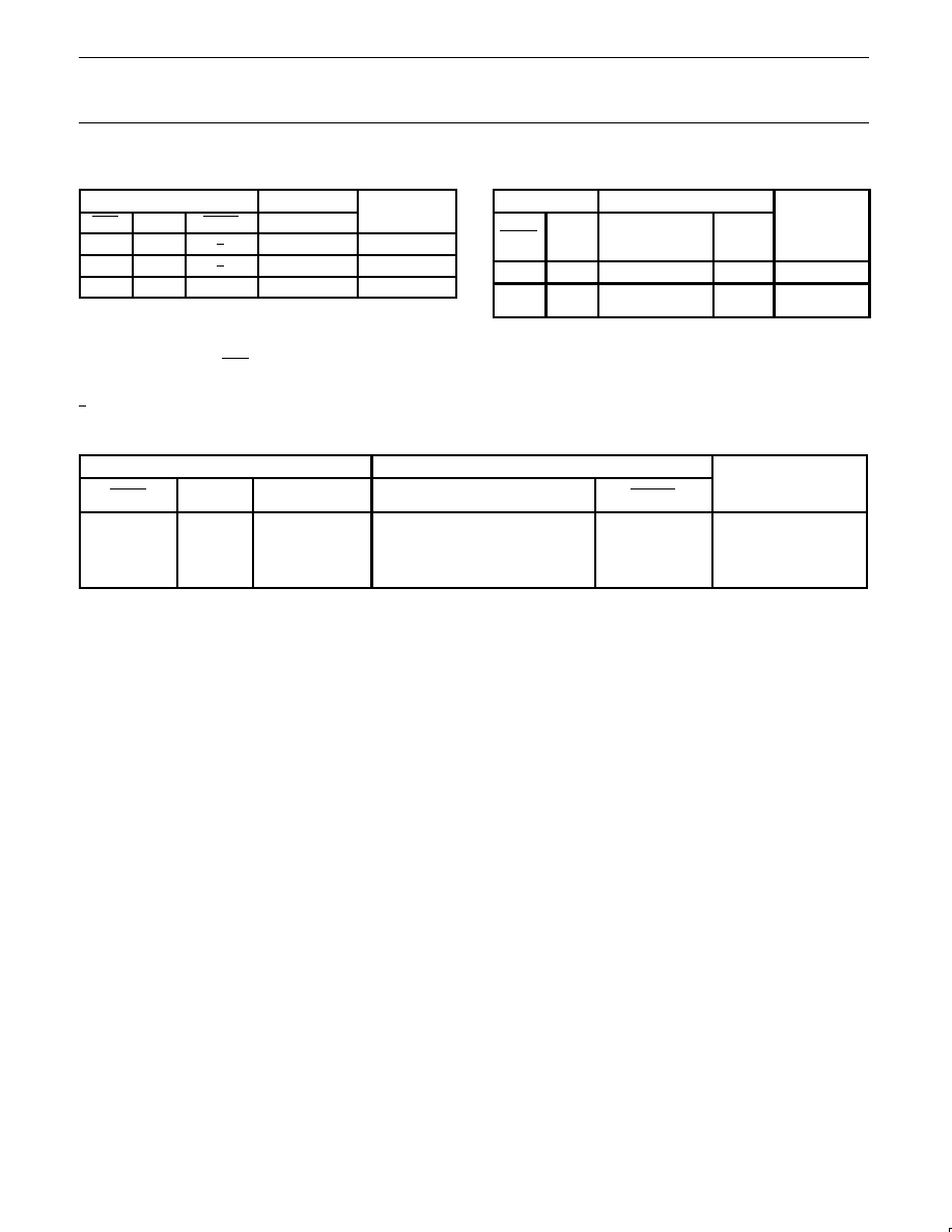
LOGIC SYMBOL
26
27
28
V
CC
= Pin 8
GND = Pin 22
18
17
16
15
14
13
12
21
20
SF01041
CPS
B0
B1
B4
B5
B6
B7
CES
A0
A1
A4
A5
A6
A7
B2
B3
A3
A2
1
2
3
4
25
11
6
7
CER
CPR
19
5
OEBR
OEAS
24
9
FR
23
10
FS
PARITY
ERROR
PIN CONFIGURATION
SF01039
1
2
3
4
5
6
7
8
9
10
11
12
17
18
19
20
21
22
23
24
25
26
27
28
B4
B5
B6
OEBR
CPR
CER
ERROR
FS
A7
B3
B2
B1
B0
FR
PARITY
GND
CPS
CES
OEAS
A0
A1
A6
13
16 A2
A5
14
15 A3
A4
B7
V
CC
LOGIC SYMBOL (IEEE/IEC)
25
26
27
28
1
2
3
4
18
17
16
15
14
13
12
11
1C2
EN1'
EN6
6C4
EN3
EN6
SF01040
1,2,6
3,4,6
20
6
7
5
21
19
5,6
5,6
6
6,7
5
23
9
10
14
XCVR
Z7

Philips Semiconductors
Product specification
74F552
Octal registered transceiver with parity and flags (3-State)
1991 Jan 02
3
INPUT AND OUTPUT LOADING AND FAN-OUT TABLE
PINS
DESCRIPTION
74F(U.L.)
HIGH/LOW
LOAD VALUE
HIGH/LOW
A0≠A7
A Data inputs
3.5/1.0
70
µ
A/0.6mA
B0≠B7
B Data inputs
3.5/1.0
70
µ
A/0.6mA
CPR
R registers clock input (active rising edge)
1.0/1.0
20
µ
A/0.6mA
CPS
S registers clock input (active rising edge)
1.0/1.0
20
µ
A/0.6mA
CER
R registers clock Enable input (active Low)
1.0/1.0
20
µ
A/0.6mA
CES
S registers clock Enable input (active Low)
1.0/1.0
20
µ
A/0.6mA
OEBR
A-to-B Output Enable input (active Low)
and clear FS output (active Low)
1.0/2.0
20
µ
A/1.2mA
OEAS
B-to-A Output Enable input (active Low)
and clear FR output (active Low)
1.0/2.0
20
µ
A/1.2mA
PARITY
Parity bit transceiver input
3.5/1.0
70
µ
A/0.6mA
PARITY
Parity bit transceiver output
750/106.7
15mA/64mA
ERROR
Parity check output (active Low)
50/33.3
1.0mA/20mA
A0≠A7
A Data outputs
150/40
3.0mA/24mA
B0≠B7
B Data outputs
750/106.7
15mA/64mA
FR
A-to-B Status Flag output (active High)
50/33.3
1.0mA/20mA
FS
B-to-A Status Flag output (active High)
50/33.3
1.0mA/20mA
NOTE: One (1.0) FAST Unit Load is defined as: 20
µ
A in the High state and 0.6mA in the Low state.
FUNCTIONAL DESCRIPTION
Data applied to the A inputs are entered and stored on the rising
edge of the CPR clock pulse, provided that the CER is Low;
simultaneously, the status flip-flop is set and the A-to-B flag (FR)
output goes High. As the CER returns to High, the data will be held
in R register. This data entered from the A inputs will appear at the B
port I/O pins after the OEBR has gone Low. When OEBR is Low, a
parity bit appears at the PARITY pin, which will be set High when
there is an even number of 1s or all 0s at the Q outputs of the R
register. After the data is assimilated, the receiving system clears
the flag FR, by changing the signal at the OEBR pin from Low to
High. Data flow from B-to-A proceeds in the same manner described
for A-to-B flow. A Low at the CES pin and a Low-to-High transition at
the CPS pin enters the B input data and the parity input data into the
S register and the parity register respectively and set the flag output
FS to High. A Low signal at the OEAS pin enables the A port I/O
pins and a Low-to-High transition of the OEAS signal clears the FS
flag. When OEAS is Low, the parity check output ERROR will be
High if there is an odd number of 1s at the Q outputs of the S
register and the parity register.
R or S REGISTER FUNCTION TABLE
INPUTS
OUTPUTS
OPERATING
An or Bn
CPX
CEX
INTERNAL Q
MODE
X
X
H
NC
Hold data
L
H
L
L
L
H
Load data
X
L
NC
Keep old data
H = High voltage level
L = Low voltage level
NC= No change
X = Don't care
X = R or S for CPX and CEX
= Low-to-High transition
= Not Low-to-High transition
OUTPUT CONTROL TABLE
INPUT
OUTPUTS
OPERATING
OEXX
INTERNAL Q
An or Bn
MODE
H
X
Z
Disable outputs
L
L
L
H
L
H
Enable outpus
H = High voltage level
L = Low voltage level
X = Don't care
XX= AS or BR
Z = High impedance "off" state
Philips Semiconductors
Product specification
74F552
Octal registered transceiver with parity and flags (3-State)
1991 Jan 02
4
R or S FLAG FUNCTION TABLE
INPUTS
OUTPUTS
OPERATING
CEX
CPX
OEXX
FR or FS
MODE
H
X
NC
Hold flag
L
H
Set flag
X
X
L
Clear flag
H = High voltage level
L = Low voltage level
NC= No change
X = Don't care
X = R or S for CPX and CEX
XX= AS or BR
= Low-to-High transition
= Not Low-to-High transition
PARITY GENERATION FUNCTION TABLE
INPUTS
OUTPUTS
OEBR
CPR
Number of Highs
in the Q outputs
of the R register
PARITY
OPERATING
MODE
H
X
X
Z
Hold flag
L
L
0,2,4,6,8
1,3,5,7
H
L
Load data
H = High voltage level
L = Low voltage level
X = Don't care
Z = High impedance "off" state
= Low-to-High transition
PARITY CHECK FUNCTION TABLE
INPUTS
OUTPUTS
OEAS
CPS
PARITY
Number of Highs in the Q outputs
of the R register
ERROR
OPERATING MODE
H
L
L
L
L
X
X
L
L
H
H
X
0,2,4,6,8
1,3,5,7
0,2,4,6,8
1,3,5,7
H
L
H
H
L
Parity check
H = High voltage level
L = Low voltage level
X = Don't care
= Low-to-High transition
Philips Semiconductors
Product specification
74F552
Octal registered transceiver with parity and flags (3-State)
1991 Jan 02
5
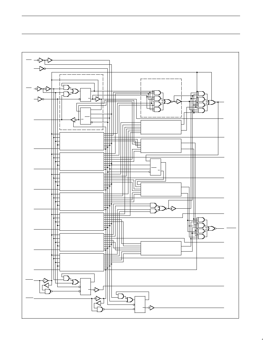
LOGIC DIAGRAM
VCC =
Pin 8
GND =
Pin 22
SF01042
D
Q
CP
Q
Q
D
CP
Q
SEL
SEL
DETAIL A
DETAIL A
DETAIL A
DETAIL A
DETAIL A
DETAIL A
DETAIL A
DETAIL A
Q
D
CLR Q
CP
Q
D
CLR Q
CP
O
D
CP
Q
SEL
SEL
CES
CPS
CER
CPR
A0
A1
A2
A3
A4
A5
A6
A7
OEBR
OEAS
FS
FR
B7
B6
ERROR
B5
B4
B3
B2
B1
B0
PARITY
21
20
7
6
18
17
16
15
14
13
12
11
5
19
23
25
26
27
28
1
2
9
3
4
24
10
DETAIL B
DETAIL B
DETAIL B
DETAIL B
DETAIL B
Philips Semiconductors
Product specification
74F552
Octal registered transceiver with parity and flags (3-State)
1991 Jan 02
6
ABSOLUTE MAXIMUM RATINGS
(Operation beyond the limits set forth in this table may impair the useful life of the device.
Unless otherwise noted these limits are over the operating free-air temperature range.)
SYMBOL
PARAMETER
RATING
UNIT
V
CC
Supply voltage
≠0.5 to +7.0
V
V
IN
Input voltage
≠0.5 to +7.0
V
I
IN
Input current
≠30 to +V
CC
mA
V
OUT
Voltage applied to output in High output state
≠0.5 to +V
CC
V
FR, FS, ERROR
40
mA
I
OUT
Current applied to output in Low output state
A0≠A7
48
mA
B0≠B7, PARITY
128
mA
T
amb
Operating free-air temperature range
0 to +70
∞
C
T
stg
Storage temperature
≠65 to +150
∞
C
RECOMMENDED OPERATING CONDITIONS
SYMBOL
PARAMETER
LIMITS
UNIT
SYMBOL
PARAMETER
MIN
NOM
MAX
UNIT
V
CC
Supply voltage
4.5
5.0
5.5
V
V
IH
High-level input voltage
2.0
V
V
IL
Low-level input voltage
0.8
V
I
IK
Input clamp current
≠18
mA
FR, FS, ERROR
≠1
mA
I
OH
High-level output current
A0≠A7
≠3
mA
B0≠B7, PARITY
≠15
mA
FR, FS, ERROR
20
mA
I
OL
Low-level output current
A0≠A7
24
mA
B0≠B7, PARITY
64
mA
T
amb
Operating free-air temperature range
0
70
∞
C

Philips Semiconductors
Product specification
74F552
Octal registered transceiver with parity and flags (3-State)
1991 Jan 02
7
DC ELECTRICAL CHARACTERISTICS
(Over recommended operating free-air temperature range unless otherwise noted.)
NO TAG
LIMITS
SYMBOL
PARAMETER
TEST CONDITIONS
NO TAG
MIN
TYP
NO TAG
MAX
UNIT
FR FS ERROR
I
O
= 1mA
±
10%V
CC
2.5
V
FR, FS, ERROR
I
OH
= ≠1mA
±
5%V
CC
2.7
3.4
V
V
O
High-level output
A0 A7
V
CC
= MIN,
V
IL
= MAX
I
O
= 3mA
±
10%V
CC
2.4
V
V
OH
g
voltage
A0≠A7
V
IL
= MAX,
V
IH
= MIN
I
OH
= ≠3mA
±
5%V
CC
2.7
3.3
V
B0 B7 PARITY
I
O
= 15mA
±
10%V
CC
2.0
V
B0≠B7, PARITY
I
OH
= ≠15mA
±
5%V
CC
2.0
V
FR FS ERROR
I
O
= 20mA
±
10%V
CC
0.30
0.50
V
FR. FS. ERROR
I
OL
= 20mA
±
5%V
CC
0.30
0.50
V
V
O
Low-level output
A0 A7
V
CC
= MIN,
V
IL
= MAX
I
O
= 24mA
±
10%V
CC
0.35
0.50
V
V
OL
voltage
A0≠A7
V
IL
= MAX,
V
IH
= MIN
I
OL
= 24mA
±
5%V
CC
0.35
0.50
V
B0 B7 PARITY
I
OL
= 48mA
±
10%V
CC
0.38
0.55
V
B0≠B7, PARITY
I
OL
= 64mA
±
5%V
CC
0.42
0.55
V
V
IK
Input clamp voltage
V
CC
= MIN, I
I
= I
IK
≠0.73
≠1.2
V
Input current at
others
V
CC
= MAX, V
I
= 7.0V
100
µ
A
I
I
maximum input
voltage
A0≠A7, B0≠B7,
PARITY
V
CC
= 5.5V, V
I
= 5.5V
1
mA
I
IH
High-level input
current
others except
A0≠A7, B0≠B7,
PARITY
V
CC
= MAX, V
I
= 2.7V
20
µ
A
I
Low-level input
others
V
CC
= MAX V = 0 5V
≠0.6
mA
I
IL
current
OEAS, OEBA
V
CC
= MAX, V
I
= 0.5V
≠1.2
mA
I
OZH
+I
IH
Off-state output current
High-level voltage applied
A0≠A7,
B0≠B7
V
CC
= MAX, V
O
= 2.7V
70
µ
A
I
OZL
+I
IL
Off-state output current
Low-level voltage applied
B0≠B7,
PARITY
V
CC
= MAX, V
O
= 0.5V
≠600
µ
A
I
OS
Short-circuit
output
A0≠A7, FS, FR,
ERROR
V
CC
= MAX
≠60
≠150
mA
OS
current
NO TAG
B0≠B7, PARITY
CC
≠100
≠225
mA
I
CCH
115
170
mA
I
CC
Supply current
(total)
I
CCL
V
CC
= MAX
125
185
mA
(total)
I
CCZ
120
180
mA
NOTES:
1. For conditions shown as MIN or MAX, use the appropriate value under the recommended operating conditions for the applicable type.
2. All typical values are at V
CC
= 5V, T
amb
= 25
∞
C.
3. Not more than one output should be shorted at a time. For testing I
OS
, the use of high-speed test apparatus and/or sample-and-hold
techniques are preferable in order to minimize internal heating and more accurately reflect operational values. Otherwise, prolonged shorting
of a High output may raise the chip temperature well above normal and thereby cause invalid readings in other parameter tests. In any
sequence of parameter tests, I
OS
should be performed last.
Philips Semiconductors
Product specification
74F552
Octal registered transceiver with parity and flags (3-State)
1991 Jan 02
8
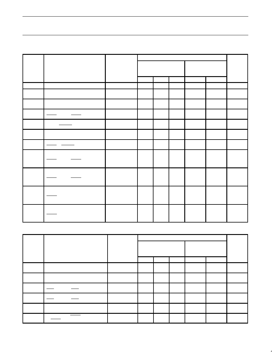
AC ELECTRICAL CHARACTERISTICS
LIMITS
TEST
T
amb
= +25
∞
C
T
amb
= 0
∞
C to +70
∞
C
SYMBOL
PARAMETER
TEST
CONDITIONS
V
CC
= +5.0V
V
CC
= +5.0V
±
10%
UNIT
CONDITIONS
C
L
= 50pF, R
L
= 500
C
L
= 50pF, R
L
= 500
MIN
TYP
MAX
MIN
MAX
f
MAX
Maximum Clock Frequency
Waveform 1
70
85
60
MHz
t
PLH
t
PHL
Propagation delay
CPS to An or CPR to Bn
Waveform 1
3.5
4.0
5.0
6.0
8.0
9.0
3.0
3.5
8.5
9.0
ns
ns
t
PLH
Propagation delay
CPS to FS or CPR to FR
Waveform 1
3.0
5.0
7.5
2.5
8.5
ns
t
PHL
Propagation delay
OEAS to FS or OEBR to FR
Waveform 2
4.0
6.0
8.5
3.5
9.0
ns
t
PLH
t
PHL
Propagation delay
CPS to ERROR
Waveform 4
6.5
7.5
13.0
11.5
16.5
15.0
6.0
7.0
18.0
16.0
ns
ns
t
PLH
t
PHL
Propagation delay
CPR to PARITY
Waveform 4
6.5
10.5
8.5
13.5
11.0
17.0
5.5
10.0
12.5
18.0
ns
ns
t
PLH
t
PHL
Propagation delay
OEAS to ERROR
Waveform
NO TAG
3.5
3.0
5.5
5.0
8.0
7.0
3.0
2.5
8.5
8.0
ns
ns
t
PZH
t
PZL
Output Enable time
OEAS to An or OEBR to Bn
Waveform
NO TAG
Waveform
NO TAG
2.5
4.0
4.0
6.5
7.0
9.5
2.0
4.0
8.0
10.5
ns
ns
t
PHZ
t
PLZ
Output Disable time
OEAS to An or OEBR to Bn
Waveform
NO TAG
Waveform
NO TAG
2.0
2.0
4.0
3.5
7.0
7.0
1.5
1.5
8.5
7.5
ns
ns
t
PZH
t
PZL
Output Enable time
OEBR to PARITY
Waveform
NO TAG
Waveform
NO TAG
2.0
4.0
4.0
5.5
7.0
8.0
2.0
3.0
7.5
9.0
ns
ns
t
PHZ
t
PLZ
Output Disable time
OEBR to PARITY
Waveform
NO TAG
Waveform
NO TAG
2.0
2.0
4.0
4.0
7.0
7.5
2.0
2.0
7.5
8.0
ns
ns
AC ELECTRICAL CHARACTERISTICS
LIMITS
TEST
T
amb
= +25
∞
C
T
amb
= 0
∞
C to +70
∞
C
SYMBOL
PARAMETER
TEST
CONDITIONS
V
CC
= +5.0V
V
CC
= +5.0V
±
10%
UNIT
CONDITIONS
C
L
= 50pF, R
L
= 500
C
L
= 50pF, R
L
= 500
MIN
TYP
MAX
MIN
MAX
t
s
(H)
t
s
(L)
Setup time, High or Low
An or Bn or PARITY to CPS or CPR
Waveform 5
7.5
4.5
8.5
5.5
ns
t
h
(H)
t
h
(L)
Hold time, High or Low
An or Bn or PARITY to CPS or CPR
Waveform 5
0
0
0
0
ns
t
s
(H)
t
s
(L)
Setup time, High or Low
CES to CPS or CER to CPR
Waveform 5
7.0
7.0
7.5
7.5
ns
t
h
(H)
t
h
(L)
Hold time, High or Low
CES to CPS or CER to CPR
Waveform 5
0
0
0
0
ns
t
w
(H)
t
w
(L)
CPS or CPR Pulse width,
High or Low
Waveform 1
5.0
6.5
6.5
7.5
ns
t
REC
Recovery time OEBR to CPR
or OEAS to CPS
Waveform 6
14.5
16.5
ns

Philips Semiconductors
Product specification
74F552
Octal registered transceiver with parity and flags (3-State)
1991 Jan 02
9
AC WAVEFORMS
For all waveforms, V
M
= 1.5V.
The shaded areas indicate when the input is permitted ot change for predictable output.
VM
VM
CPS,
CPR
An, Bn
FS, FR
VM
tPLH
SF01043
VM
tPHL
tW
(L)
tW
(H)
1/fMAX
Waveform 1. Propagation Delay, Clock Input to Output and
Maximum Clock Frequency
VM
OEAS, OEBR
FS, FR
SF01044
tPHL
VM
Waveform 2. Propagation Delay, Output Enable to Flag Output
V
M
V
M
V
M
V
M
t
PLH
t
PHL
OEAS
SF01045
ERROR
Waveform 3. Propagation Delay, Output Enable to ERROR
t
PLH
t
PHL
V
M
V
M
CPS,
CPR
PARITY
V
M
SF01046
V
M
V
M
V
M
ERROR
t
PHL
t
PLH
Waveform 4. Propagation Delay, Clock to PARITY and ERROR
SF01047
V
M
V
M
V
M
V
M
V
M
V
M
t
s
(L)
t
s
(H)
t
h
(L)
t
h
(H)
An, Bn
CES, CER
PARITY
CPS, CPR
Waveform 5. Data Setup and Hold Times
VM
OEAS, OEBR
CPS,
CPR
SF01048
tREC
VM
Waveform 6. Recovery Time from Output Enable to Clock
V
M
V
M
V
M
t
PHZ
t
PZH
OEAS, OEBR
An, Bn
PARITY
V
OH
-0.3V
0V
SF01049
Waveform 7. 3-State Output Enable Time to High Level
and Output Disable Time from High Level
V
M
V
M
V
M
t
PLZ
t
PZL
OEAS, OEBR
An, Bn
PARITY
V
OL
+0.3V
SF01050
Waveform 8. 3-State Output Enable Time to Low Level
and Output Disable Time from Low Level

Philips Semiconductors
Product specification
74F552
Octal registered transceiver with parity and flags (3-State)
1991 Jan 02
10
TEST CIRCUIT AND WAVEFORM
tw
90%
VM
10%
90%
VM
10%
90%
VM
10%
90%
VM
10%
NEGATIVE
PULSE
POSITIVE
PULSE
tw
AMP (V)
0V
0V
tTHL (tf
)
INPUT PULSE REQUIREMENTS
rep. rate
t
w
t
TLH
t
THL
1MHz
500ns
2.5ns
2.5ns
Input Pulse Definition
VCC
family
74F
D.U.T.
PULSE
GENERATOR
RL
CL
RT
VIN
VOUT
Test Circuit for 3-State Outputs
DEFINITIONS:
R
L
= Load resistor;
see AC electrical characteristics for value.
C
L
= Load capacitance includes jig and probe capacitance;
see AC electrical characteristics for value.
R
T
= Termination resistance should be equal to Z
OUT
of
pulse generators.
tTHL (tf
)
tTLH (tr
)
tTLH (tr
)
AMP (V)
amplitude
3.0V
1.5V
V
M
RL
7.0V
SF00777
TEST
SWITCH
t
PLZ
closed
t
PZL
closed
All other
open
SWITCH POSITION

Philips Semiconductors
Product specification
74F552
Octal registered transceiver with parity and flags (3-State)
1991 Jan 02
11
DIP28:
plastic dual in-line package; 28 leads (600 mil); long body
SOT117-2
Philips Semiconductors
Product specification
74F552
Octal registered transceiver with parity and flags (3-State)
1991 Jan 02
12
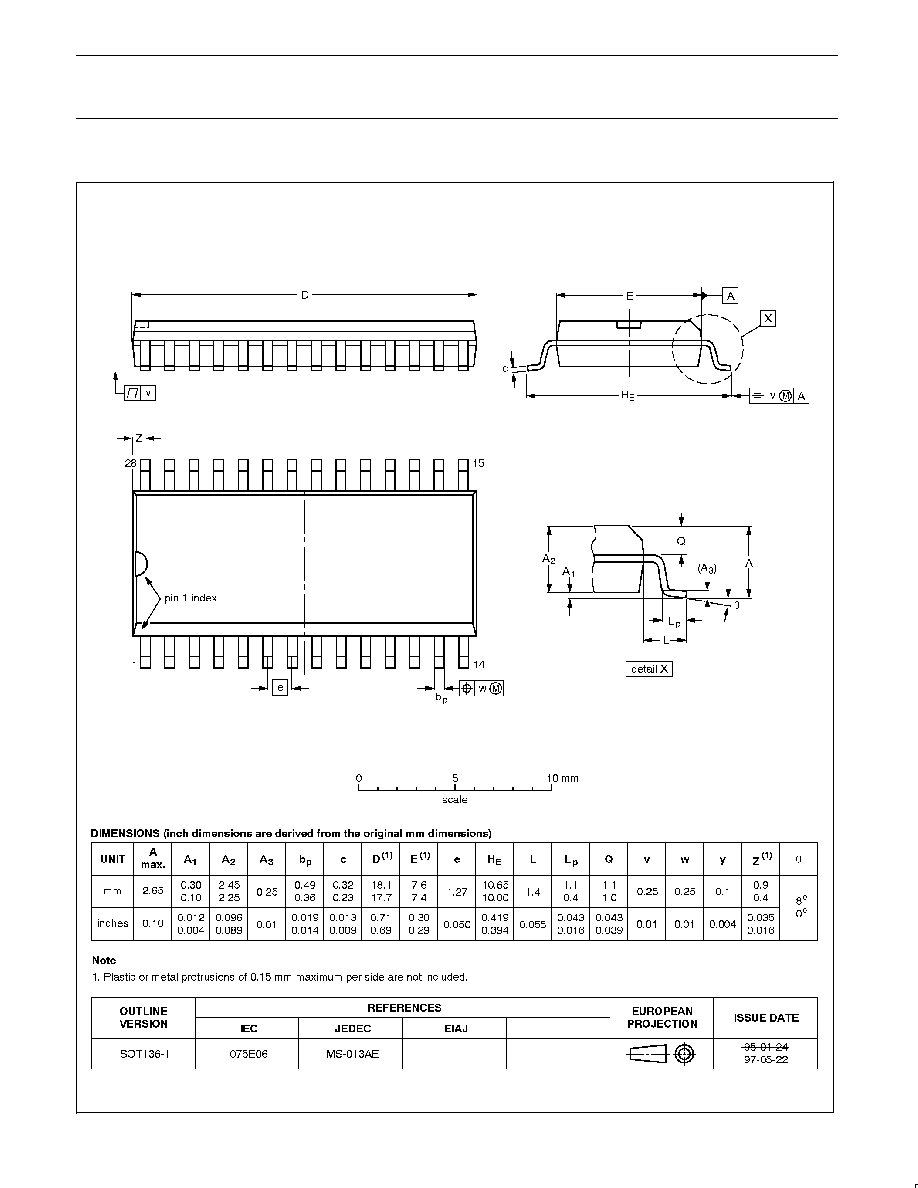
SO28:
plastic small outline package; 28 leads; body width 7.5mm
SOT136-1

Philips Semiconductors
Product specification
74F552
Octal registered transceiver with parity and flags (3-State)
1991 Jan 02
13
NOTES
Philips Semiconductors
Product specification
74F552
Octal registered transceiver with parity and flags (3-State)
yyyy mmm dd
14
Definitions
Short-form specification -- The data in a short-form specification is extracted from a full data sheet with the same type number and title. For
detailed information see the relevant data sheet or data handbook.
Limiting values definition -- Limiting values given are in accordance with the Absolute Maximum Rating System (IEC 134). Stress above one
or more of the limiting values may cause permanent damage to the device. These are stress ratings only and operation of the device at these or
at any other conditions above those given in the Characteristics sections of the specification is not implied. Exposure to limiting values for extended
periods may affect device reliability.
Application information -- Applications that are described herein for any of these products are for illustrative purposes only. Philips
Semiconductors make no representation or warranty that such applications will be suitable for the specified use without further testing or
modification.
Disclaimers
Life support -- These products are not designed for use in life support appliances, devices or systems where malfunction of these products can
reasonably be expected to result in personal injury. Philips Semiconductors customers using or selling these products for use in such applications
do so at their own risk and agree to fully indemnify Philips Semiconductors for any damages resulting from such application.
Right to make changes -- Philips Semiconductors reserves the right to make changes, without notice, in the products, including circuits, standard
cells, and/or software, described or contained herein in order to improve design and/or performance. Philips Semiconductors assumes no
responsibility or liability for the use of any of these products, conveys no license or title under any patent, copyright, or mask work right to these
products, and makes no representations or warranties that these products are free from patent, copyright, or mask work right infringement, unless
otherwise specified.
Philips Semiconductors
811 East Arques Avenue
P.O. Box 3409
Sunnyvale, California 94088≠3409
Telephone 800-234-7381
©
Copyright Philips Electronics North America Corporation 1998
All rights reserved. Printed in U.S.A.
print code
Date of release: 10-98
Document order number:
9397-750-05137
Philips
Semiconductors
Data sheet
status
Objective
specification
Preliminary
specification
Product
specification
Product
status
Development
Qualification
Production
Definition
[1]
This data sheet contains the design target or goal specifications for product development.
Specification may change in any manner without notice.
This data sheet contains preliminary data, and supplementary data will be published at a later date.
Philips Semiconductors reserves the right to make chages at any time without notice in order to
improve design and supply the best possible product.
This data sheet contains final specifications. Philips Semiconductors reserves the right to make
changes at any time without notice in order to improve design and supply the best possible product.
Data sheet status
[1]
Please consult the most recently issued datasheet before initiating or completing a design.