 | –≠–ª–µ–∫—Ç—Ä–æ–Ω–Ω—ã–π –∫–æ–º–ø–æ–Ω–µ–Ω—Ç: N74F564D | –°–∫–∞—á–∞—Ç—å:  PDF PDF  ZIP ZIP |
Philips
Semiconductors
74F564
Octal D flip-flop (3-State)
Product specification
1996 Jan 05
INTEGRATED CIRCUITS
IC15 Data Handbook
Philips Semiconductors
Product specification
74F564
Octal D flip-flop (3-State)
2
1996 Jan 05
853-0166 16189
FEATURES
∑
74F564 is broadside pinout version of 74F534
∑
Inputs and Outputs on opposite side of package allow easy
interface to Microprocessors
∑
Useful as an Input or Ouput port for Microprocessors
∑
3-State Ouputs for Bus interfacing
∑
Common Output Enable
∑
74F574 is a non-inverting version of 74F564
DESCRIPTION
The 74F564 has a broadside pinout configuration to facilitate PC
board layout and allows easy interface with microprocessors.
It is an 8-bit, edge triggered register coupled to eight 3-State output
buffers. The two sections of the device are controlled independently
by the clock (CP) and Output Enable (OE) control gates.
The register is fully edge-triggered. The state of each D input, one
setup time before the Low-to-High clock transition is transferred to
the corresponding flip-flop's Q output.
The 3-State output buffers are designed to drive heavily loaded
3-State buses, MOS memories, or MOS microprocessors. The
active Low Output Enable (OE) controls all eight 3-State buffers
independently of the register operation. When OE is Low, data in the
register appears at the outputs. When OE is High, the outputs are in
high impedance "off" state, which means they will neither drive nor
load the bus.
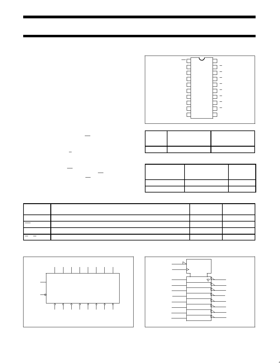
PIN CONFIGURATION
1
2
3
4
5
6
7
8
9
10
11
12
13
14
15
16
17
18
19
20
OE
GND
VCC
CP
SF01052
Q0
D0
D1
Q1
D2
Q2
Q3
D3
Q4
D4
Q5
D5
Q6
D6
Q7
D7
TYPE
TYPICAL f
MAX
TYPICAL SUPPLY
CURRENT
(TOTAL)
74F564
180MHz
50mA
ORDERING INFORMATION
DESCRIPTION
COMMERCIAL RANGE
V
CC
= 5V
±
10%,
T
amb
= 0
∞
C to +70
∞
C
PKG.
DWG #
20-Pin Plastic DIP
N74F564N
SOT146-1
20-Pin Plastic SOL
N74F564D
SOT163-1
INPUT AND OUTPUT LOADING AND FAN-OUT TABLE
PINS
DESCRIPTION
74F (U.L.)
HIGH/LOW
LOAD VALUE
HIGH/LOW
D0 - D7
Data inputs
1.0/1.0
20
µ
A/0.6mA
OE
Output Enable input (active Low)
1.0/1.0
20
µ
A/0.6mA
CP
Clock Pulse input (active rising edge)
1.0/1.0
20
µ
A/0.6mA
Q0 - Q7
3-State outputs
150/40
3.0mA/24mA
NOTE: One (1.0) FAST Unit Load (U.L.) is defined as: 20
µ
A in the High state and 0.6mA in the Low state.
LOGIC SYMBOL
3
4
5
6
7
8
14
15
16
17
18
19
1
11
CP
OE
Q0
D0
D1
Q1
D2
Q2
Q3
D3
Q4
D4
Q5
D5
9
2
12
13
Q6
D6
Q7
D7
SF01053
V
CC
=Pin 20
GND=Pin 10
LOGIC SYMBOL (IEEE/IEC)
1
2D
EN1
1
SF01054
11
C2
2
3
4
5
6
7
8
9
19
18
17
16
15
14
13
12
Philips Semiconductors
Product specification
74F564
Octal D flip-flop (3-State)
1996 Jan 05
3
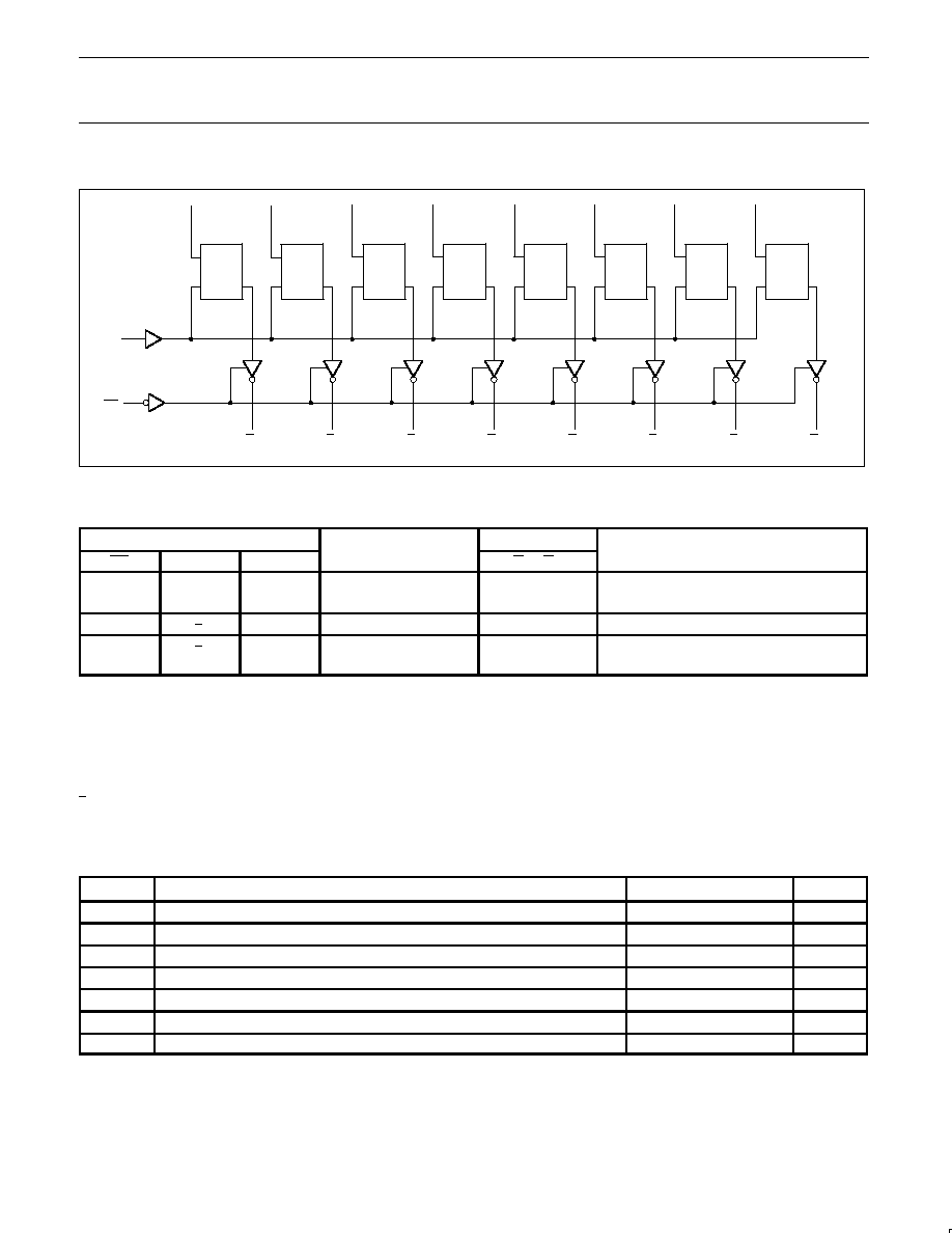
LOGIC DIAGRAM
D0
D1
D2
D3
D4
D5
D6
D7
Q0
Q1
Q2
Q3
Q4
Q5
Q6
Q7
CP
OE
2
3
4
5
6
7
8
9
12
13
14
15
16
17
18
19
1
11
CP
D
Q
CP
D
Q
CP
Q
D
CP
D
Q
CP
D
Q
CP
D
Q
CP
D
Q
CP
D
Q
V
CC
=Pin 20
GND=Pin 10
SF01055
FUNCTION TABLE
INPUTS
INTERNAL
OUTPUTS
OPERATING MODES
OE
CP
Dn
REGISTER
Q0 ≠ Q7
OPERATING MODES
L
L
l
h
L
H
H
L
Load and read register
L
X
NC
NC
Hold
H
H
X
Dn
NC
Dn
Z
Z
Disable outputs
H = High voltage level
h = High voltage level one setup time prior to the Low-to-High clock transition
L = Low voltage level
l
= Low voltage level one setup time prior to the Low-to-High clock transition
NC= No change
X = Don't care
Z = High impedance "off" state
= Low-to-High clock transition
= Not a Low-to-High clock transition
ABSOLUTE MAXIMUM RATINGS
(Operation beyond the limits set forth in this table may impair the useful life of the device.
Unless otherwise noted these limits are over the operating free-air temperature range.)
SYMBOL
PARAMETER
RATING
UNIT
V
CC
Supply voltage
≠0.5 to +7.0
V
V
IN
Input voltage
≠0.5 to +7.0
V
I
IN
Input current
≠30 to +5.0
mA
V
OUT
Voltage applied to output in High output state
≠0.5 to +V
CC
V
I
OUT
Current applied to output in Low output state
48
mA
T
amb
Operating free-air temperature range
0 to +70
∞
C
T
stg
Storage temperature
≠65 to +150
∞
C

Philips Semiconductors
Product specification
74F564
Octal D flip-flop (3-State)
1996 Jan 05
4
RECOMMENDED OPERATING CONDITIONS
SYMBOL
PARAMETER
LIMITS
UNIT
SYMBOL
PARAMETER
MIN
NOM
MAX
UNIT
V
CC
Supply voltage
4.5
5.0
5.5
V
V
IH
High-level input voltage
2.0
V
V
IL
Low-level input voltage
0.8
V
I
IK
Input clamp current
≠18
mA
I
OH
High-level output current
≠3
mA
I
OL
Low-level output current
24
mA
T
amb
Operating free-air temperature range
0
70
∞
C
DC ELECTRICAL CHARACTERISTICS
(Over recommended operating free-air temperature range unless otherwise noted.)
NO TAG
LIMITS
SYMBOL
PARAMETER
TEST CONDITIONS
NO TAG
MIN
TYP
NO TAG
MAX
UNIT
V
O
High level output voltage
V
CC
= MIN, V
IL
= MAX,
±
10%V
CC
2.4
V
V
OH
High-level output voltage
V
CC
MIN, V
IL
MAX,
V
IH
= MIN, I
OH
= MAX
±
5%V
CC
2.7
3.4
V
V
O
Low level output voltage
V
CC
= MIN, V
IL
= MAX,
±
10%V
CC
0.35
0.50
V
V
OL
Low-level output voltage
V
CC
MIN, V
IL
MAX,
V
IH
= MIN, I
OL
= MAX
±
5%V
CC
0.35
0.50
V
V
IK
Input clamp voltage
V
CC
= MIN, I
I
= I
IK
≠0.73
≠1.2
V
I
I
Input current at
maximum input voltage
V
CC
= MAX, V
I
= 7.0V
100
µ
A
I
IH
High-level input current
V
CC
= MAX, V
I
= 2.7V
20
µ
A
I
IL
Low-level input current
V
CC
= MAX, V
I
= 0.5V
≠0.6
mA
I
OZH
Off-state output current,
High-level voltage applied
V
CC
= MAX, V
O
= 2.7V
50
µ
A
I
OZL
Off-state output current,
Low-level voltage applied
V
CC
= MAX, V
O
= 0.5V
≠50
µ
A
I
OS
Short-circuit output current
NO TAG
V
CC
= MAX
≠60
≠150
mA
I
CCH
45
65
mA
I
CC
Supply current (total)
I
CCL
V
CC
= MAX
50
75
mA
I
CCZ
55
80
mA
NOTES:
1. For conditions shown as MIN or MAX, use the appropriate value specified under recommended operating conditions for the applicable type.
2. All typical values are at V
CC
= 5V, T
amb
= 25
∞
C.
3. Not more than one output should be shorted at a time. For testing I
OS
, the use of high-speed test apparatus and/or sample-and-hold
techniques are preferable in order to minimize internal heating and more accurately reflect operational values. Otherwise, prolonged shorting
of a High output may raise the chip temperature well above normal and thereby cause invalid readings in other parameter tests. In any
sequence of parameter tests, I
OS
tests should be performed last.
Philips Semiconductors
Product specification
74F564
Octal D flip-flop (3-State)
1996 Jan 05
5
AC ELECTRICAL CHARACTERISTICS
LIMITS
SYMBOL
PARAMETER
TEST
CONDITIONS
T
amb
= +25
∞
C
V
CC
= +5V
C
L
= 50pF, R
L
= 500
T
amb
= 0
∞
C to +70
∞
C
V
CC
= +5V
±
10%
C
L
= 50pF, R
L
= 500
UNIT
MIN
TYP
MAX
MIN
MAX
f
MAX
Maximum Clock frequency
Waveform
NO TAG
160
180
150
MHz
t
PLH
t
PHL
Propagation delay
CP to Qn
Waveform
NO TAG
3.5
3.5
5.0
5.0
8.0
8.0
3.0
3.0
8.5
8.5
ns
t
PZH
t
PZL
Output Enable time
to High or Low level
Waveform 4
Waveform 5
2.5
4.0
4.5
5.5
7.5
8.0
2.0
3.5
8.0
8.5
ns
t
PHZ
t
PLZ
Output Disable time
from High or Low level
Waveform 4
Waveform 5
1.0
1.0
3.0
2.5
6.0
5.5
1.0
1.0
7.0
6.0
ns
AC SETUP REQUIREMENTS
LIMITS
SYMBOL
PARAMETER
TEST
CONDITIONS
T
amb
= +25
∞
C
V
CC
= +5V
C
L
= 50pF, R
L
= 500
T
amb
= 0
∞
C to +70
∞
C
V
CC
= +5.0V
±
10%
C
L
= 50pF, R
L
= 500
UNIT
MIN
TYP
MAX
MIN
MAX
t
s
(H)
t
s
(L)
Setup time,
Dn to CP
Waveform 3
2.0
2.0
2.0
2.5
ns
t
h
(H)
t
h
(L)
Hold time,
Dn to CP
Waveform 3
1.0
1.0
1.5
1.5
ns
t
w
(H)
t
w
(L)
CP pulse width,
High or Low
Waveform NO TAG
3.5
3.5
3.5
3.5
ns
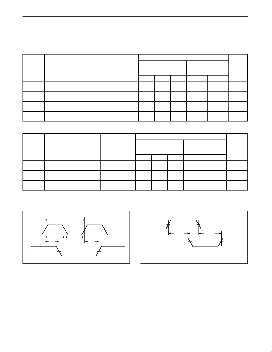
AC WAVEFORMS
For all waveforms, V
M
= 1.5V
The shaded areas indicate when the input is permitted to change for predictable output performance.
tW(H)
CP
Qn
VM
VM
VM
VM
VM
1/fMAX
tW(L)
tPLH
tPHL
SF01051
Waveform 1. Propagation Delay, Clock and Enable Inputs
to Output, Enable, Clock Pulse Widths,
and Maximum Clock Frequency
VM
VM
VM
tPHL
Dn
Qn
VM
tPLH
SF00990
Waveform 2. Propagation Delay for Data to Outputs