Philips Semiconductors
Product specification
74F569
4-bit bidirectional binary synchronous counter (3-State)
2
1996 Jan 05
853≠0376 16193
FEATURES
∑
4-bit bidirectional counting ≠ binary counter
∑
Synchronous counting and loading
∑
Look ahead carry capability for easy cascading
∑
Preset capability for programmable operation
∑
Master Reset (MR) overrides all other inputs
∑
Synchronous Reset (SR) overrides counting and parallel loading
∑
Clock Carry (CC) output to be used as a clock for flip-flops,
register and counters
∑
3-State outputs for bus organized systems
DESCRIPTION
The 74F569 is a fully synchronous Up/Down binary counter. It
features preset capabilities for programmable operation, carry look
ahead for programmable operation, carry look ahead for easy
cascading, and U/D input to control the direction of counting. For
maximum flexibility there are both Synchronous and Master Reset
inputs as well as both Clocked Carry (CC) and Terminal Count (TC)
outputs. All state changes except Master Reset are initiated by
rising edge of the clock. A High signal on the Output Enable (OE)
input forces the output buffers into the high impedance state but
does not prevent counting, resetting or parallel loading.
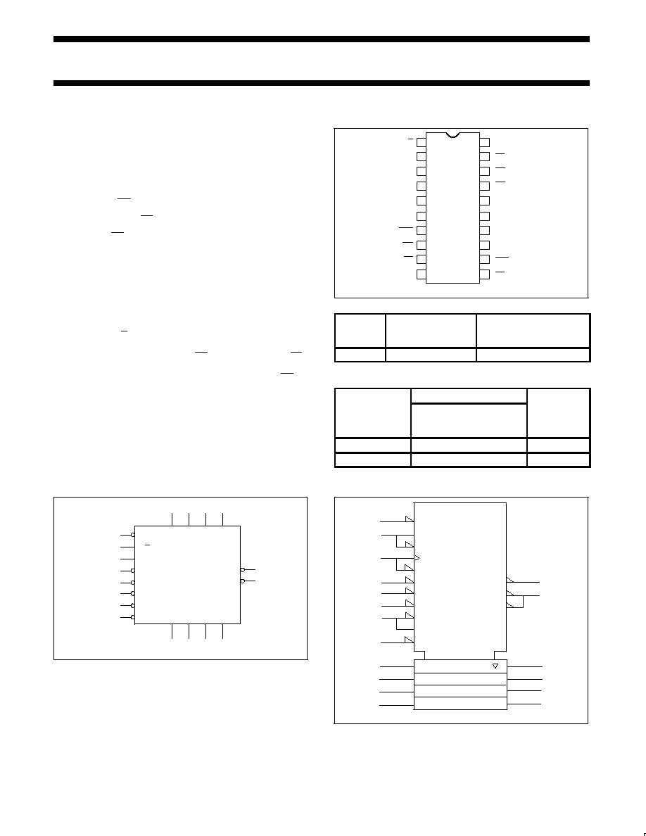
PIN CONFIGURATION
20
19
18
17
16
15
14
13
8
7
6
5
4
3
2
1
VCC
TC
Q0
Q1
Q2
Q3
CET
PE
U/D
CP
D0
D1
D2
D3
CEP
GND
SF01072
MR
SR
CC
OE
12
11
10
9
TYPE
TYPICAL f
MAX
TYPICAL
SUPPLY CURRENT
(TOTAL)
74F569
115MHz
40mA
ORDERING INFORMATION
ORDER CODE
DESCRIPTION
COMMERCIAL RANGE
V
CC
= 5V
±
10%,
T
amb
= 0
∞
C to +70
∞
C
PKG.
DWG. #
20-pin plastic DIP
N74F569N
SOT146-1
20-pin plastic SO
N74F569D
SOT163-1
LOGIC SYMBOL
11
3
4
5
6
19
13
14
15
16
1
2
7
12
CP
CEP
CET
PE
D0
D1
D2
D3
Q0
Q1
Q2
Q3
TC
U/D
SF01056
8
9
MR
SR
17
OE
18
CC
V
CC
= Pin 20
GND = Pin 10
LOGIC SYMBOL (IEEE/IEC)
M2[DOWN]
3
3,5D
EN10
SF01057
C5/1,4,7,8+/2,4,7,8≠
M1[UP]
CTR DIV 10
19
1,7(CT=15)G9
2,7(CT=0)G9
Z6
G7
10
G8
M4[COUNT]
5CT=0
M3[LOAD]
CT=0
18
6,7,8,9
4
5
6
15
14
13
16
17
1
2
12
7
9
11
8
Philips Semiconductors
Product specification
74F569
4-bit bidirectional binary synchronous counter (3-State)
1996 Jan 05
3
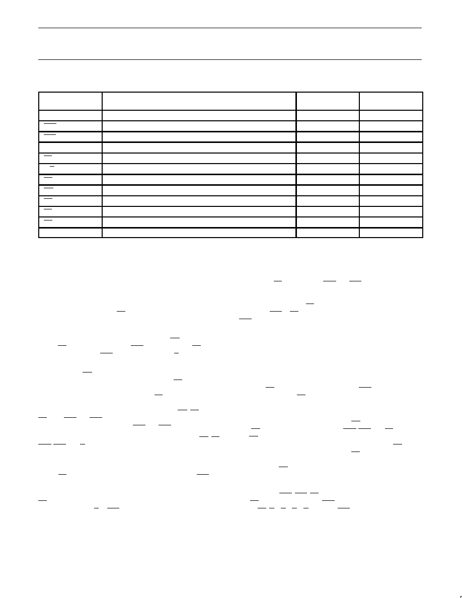
INPUT AND OUTPUT LOADING AND FAN-OUT TABLE
PINS
DESCRIPTION
74F(U.L.)
HIGH/LOW
LOAD VALUE
HIGH/LOW
D0 - D3
Parallel data inputs
1.0/1.0
20
µ
A/0.6mA
CEP
Count Enable parallel input (active Low)
1.0/1.0
20
µ
A/0.6mA
CET
Count Enable Trickle input (active Low)
1.0/2.0
20
µ
A/1.2mA
CP
Clock input (active rising edge)
1.0/1.0
20
µ
A/0.6mA
PE
Parallel Enable input (active Low)
1.0/2.0
20
µ
A/1.2mA
U/D
Up/Down count control input
1.0/1.0
20
µ
A/0.6mA
OE
Output Enable input
1.0/1.0
20
µ
A/0.6mA
MR
Master Reset input (active Low)
1.0/1.0
20
µ
A/0.6mA
SR
Synchronous Reset (active Low)
1.0/1.0
20
µ
A/0.6mA
TC
Terminal count output (active Low)
50/33
1.0mA/20mA
CC
Clocked carry output (active Low)
50/33
1.0mA/20mA
Q0 - Q3
Data outputs
150/40
3.0mA/24mA
NOTE: One (1.0) FAST Unit Load (U.L.) is defined as: 20
µ
A in the High state and 0.6mA in the Low state.
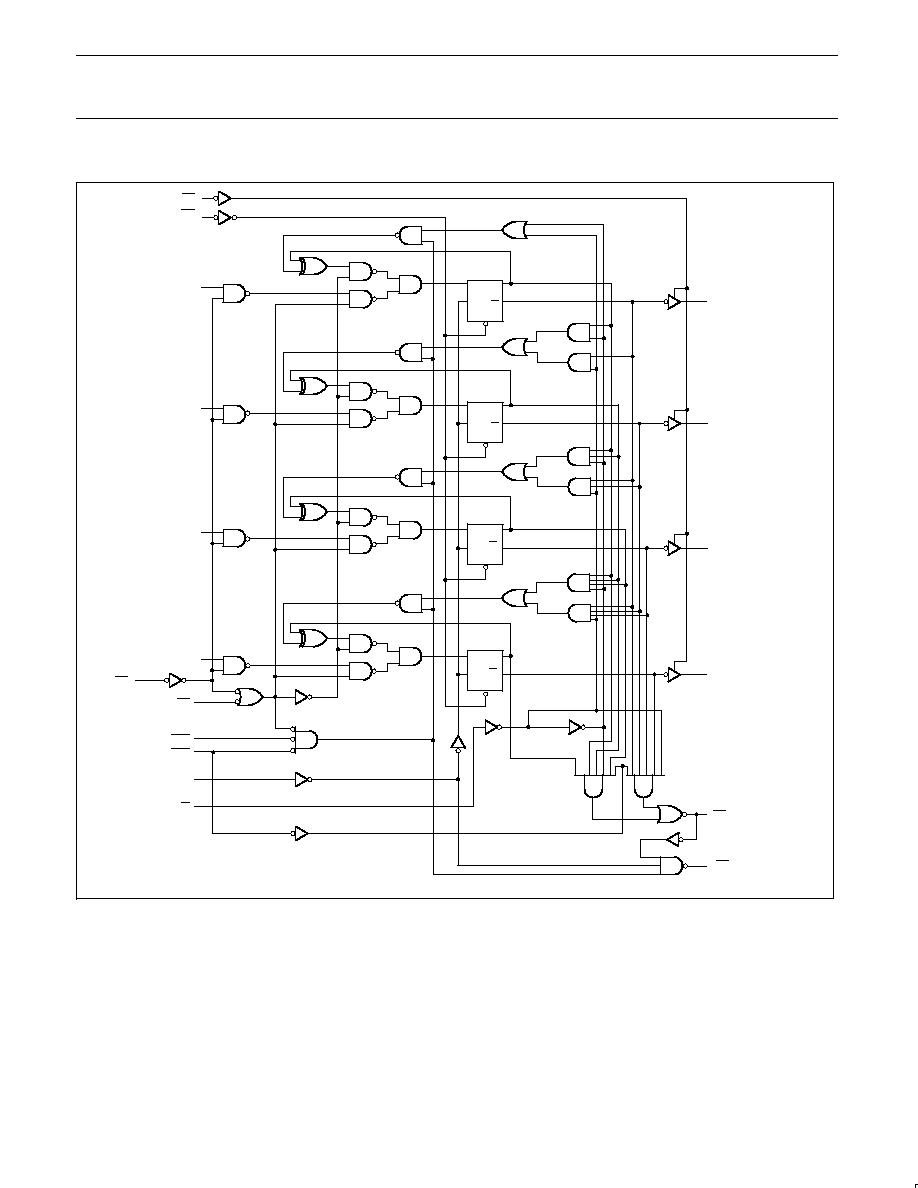
FUNCTIONAL DESCRIPTION
The 74F569 counts in the modulo-16 binary sequence. From
state 0 (LLLL) it will increment to 15 in the up mode; in the down
mode it will decrement from 15 to 0. The clock inputs of all flip-flops
are driven parallel through a clock buffer. All state changes (except
due to Master Reset) occur synchronously with the Low-to-High
transition of the Clock Pulse (CP) input.
The circuit has five fundamental modes of operation, in order of
precedence: asynchronous reset, synchronous reset, parallel load,
count and hold. Six control inputs≠Master Reset (MR), Synchronous
Reset (SR), Count Enable Trickle (CET), Parallel Enable (PE),
Count Enable Parallel (CEP), and the Up/Down (U/D) input ≠
determine the mode of operation, as shown in the Function Table.
A Low signal on MR overrides all other inputs and asynchronously
forces the flip-flop Q outputs Low. A Low signal on SR overrides
counting and parallel loading and allows the Q output to go Low on
the next rising edge of CP. A Low signal on PE overrides counting
and allows information on the parallel data (Dn) inputs to be loaded
into the flip-flops on the next rising edge of CP. With MR, SR, and
PE High, CEP and CET permit counting when both are Low.
Conversely, a High signal on either CEP and CET inhibits counting.
The 74F569 uses edge-triggered flip-flops and changing the SR, PE,
CEP, CET or U/D inputs when the CP is in either state does not
cause errors, provided that the recommended setup and hold times,
with respect to the rising edge of CP, are observed. Two types of
outputs are provided as overflow/underflow indicators. The Terminal
Count (TC) output is normally High and goes Low provided CET is
Low, when the counter reaches zero in the down mode, or reaches
maximum 15 in the up mode
TC will then remain Low until a state change occurs by counting or
presetting, or until U/D or CET is changed.
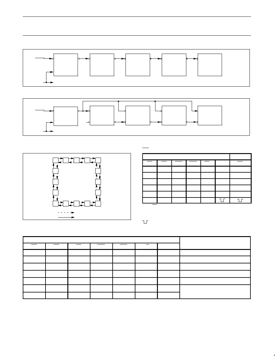
To implement synchronous multistage counters, the connections
between the TC output and the CEP and CET inputs can provide
either slow or fast carry propagation. Figure 1 shows the
connections for a simple ripple carry, in which the clock period must
be longer than the CP to TC delay of the first stage, plus the
cumulative CET to TC delays of the intermediate stages, plus the
CET to CP setup time of the last stage. This total delay plus setup
time sets the upper limit on clock frequency. For faster clock rates,
the carry look ahead connections in Figure 2 are recommended. In
this scheme the ripple delay through the intermediate stages
commences with the same clock that causes the first stage to tick
over from Max to Min in the up mode, or Min to Max in the down
mode, to start its final cycle. Since this takes 16 clocks to complete,
there is plenty of time for the ripple to progress through the
intermediate stages. The critical timing that limits the clock period is
the CP to TC delay of the first stage plus the CEP to CP setup time
of the last stage. The TC output is subject to decoding spikes due to
internal race conditions and is therefore not recommended for use
as a clock or asynchronous reset for flip-flops, register or counters.
For such applications, the Clocked Carry (CC) output is provided.
The CC output is normally High. When CEP, CET, and TC are Low,
the CC output will go Low, when the clock next goes Low and will
stay Low until the clock goes High again; as shown in the CC
Function Table. When the Output Enable (OE) is Low, the parallel
data outputs Q0≠Q3 are active and follow the flip-flop Q outputs. A
High signal on OE forces Q0≠Q3 to the High impedance state but
does not prevent counting, loading or resetting.
LOGIC EQUATIONS:
Count Enable=CEP
◊
CET
◊
PE
Up: TC=Q0
◊
Q1
◊
Q2
◊
Q3
◊
(Up)
◊
CET
Down: TC=Q0
◊
Q1
◊
Q2
◊
Q3
◊
(Down)
◊
CET
Philips Semiconductors
Product specification
74F569
4-bit bidirectional binary synchronous counter (3-State)
1996 Jan 05
4
CET
SF01059
TC
CP
CET
TC
CET
TC
CET
TC
CET
TC
COUNT
CP
TO ALL STAGES
Figure 1. Multistage Counter with Ripple Carry
CET
SF01061
TC
CP
CET
TC
CEP
CET
TC
CEP
CET
TC
CEP
CET
CEP
COUNT
CP
TO ALL STAGES
LOW
Figure 2. Multistage Counter with Look-Ahead Carry
STATE DIAGRAM
0
1
2
3
4
5
6
7
8
9
10
11
12
13
14
15
COUNT DOWN
COUNT UP
SF01058
CC FUNCTION TABLE
INPUTS
OUTPUT
SR
PE
CEP
CET
TC*
CP
CC
L
X
X
X
X
X
H
X
L
X
X
X
X
H
X
X
H
X
X
X
H
X
X
X
H
X
X
H
X
X
X
X
H
X
H
H
H
L
L
L
*
= TC is generated internally
H = High voltage level
L = Low voltage level
X = Don't care
=
Low Pulse
FUNCTION TABLE
INPUTS
OPERATING MODE
MR
SR
PE
CEP
CET
U/D
CP
OPERATING MODE
L
X
X
X
X
X
X
Asynchronous reset
h
l
X
X
X
X
Synchronous reset
h
h
l
X
X
X
Parallel load
h
h
h
l
l
h
Count Up (increment)
h
h
h
l
l
l
Count Down (decrement)
h
H
H
H
X
X
X
Hold (do nothing)
h
H
H
X
H
X
X
Hold (do nothing)
H = High voltage level
h = High voltage level one setup time prior to the Low-to-High clock transition
L = Low voltage level
l
= Low voltage level one setup time prior to the Low-to-High clock transition
X = Don't care
= Low-to-High clock transition