Philips Semiconductors
Product specification
74F573/74F574
Latch/flip-flop
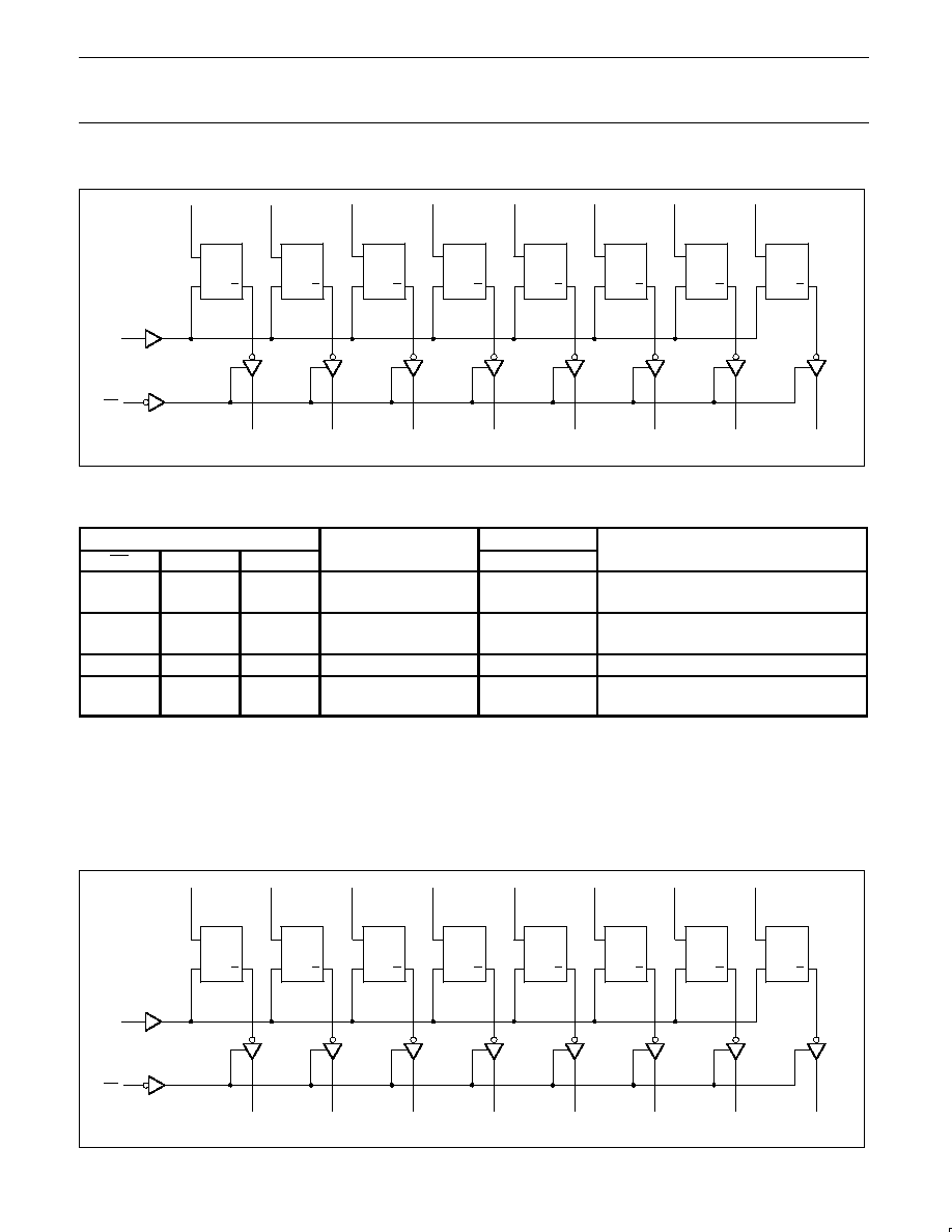
74F573 Octal Transparent Latch (3-State)
74F574 Octal D Flip-Flop (3-State)
2
1989 Oct 16
853-0083 97897
FEATURES
∑
74F573 is broadside pinout version of 74F373
∑
74F574 is broadside pinout version of 74F374
∑
Inputs and Outputs on opposite side of package allow easy
interface to Microprocessors
∑
Useful as an Input or Output port for Microprocessors
∑
3-State Outputs for Bus interfacing
∑
Common Output Enable
∑
74F563 and 74F564 are inverting version of 74F573 and 74F574
respectively
∑
3-State Outputs glitch free during power-up and power-down
∑
These are High-Speed replacements for N8TS805 and N8TS806
DESCRIPTION
The 74F573 is an octal transparent latch coupled to eight 3-State
output buffers. The two sections of the device are controlled
independently by Enable (E) and Output Enable (OE) control gates.
The 74F573 is functionally identical to the 74F373 but has a
broadside pinout configuration to facilitate PC board layout and
allow easy interface with microprocessors.
The data on the D inputs is transferred to the latch outputs when the
Enable (E) input is High. The latch remains transparent to the data
input while E is High and stores the data that is present one setup
time before the High-to-Low enable transition.
The 3-State output buffers are designed to drive heavily loaded
3-State buses, MOS memories, or MOS microprocessors. The
active Low Output Enable (OE) controls all eight 3-State buffers
independent to the latch operation. When OE is Low, the latched or
transparent data appears at the outputs. When OE is High, the
outputs are in high impedance "off" state, which means they will
neither drive nor load the bus.
The 74F574 is functionally identical to the 74F374 but has a
broadside pinout configuration to facilitate PC board layout and
allow easy interface with microprocesors.
It is an 8-bit, edge triggered register coupled to eight 3-State output
buffers. The two sections of the device are controlled independently
by the clock (CP) and Output Enable (OE) control gates.
The register is fully edge-triggered. The state of each D input, one
setup time before the Low-to-High clock transition is transferred to
the corresponding flip-flop's Q output.
The 3-State output buffers are designed to drive heavily loaded
3-State buses, MOS memories, or MOS microprocessors. The
active Low Output Enable (OE) controls all eight 3-State buffers
independently of the latch operation. When OE is Low, the latched
or transparent data appears at the outputs. When OE is High, the
outputs are in high impedance "off" state, which means they will
neither drive nor load the bus.
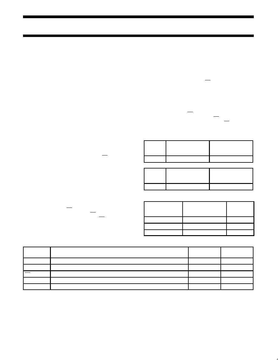
TYPE
TYPICAL
PROPAGATION DELAY
TYPICAL SUPPLY
CURRENT
(TOTAL)
74F573
5.0ns
35mA
TYPE
TYPICAL f
MAX
TYPICAL SUPPLY
CURRENT
(TOTAL)
74F574
180MHz
50mA
ORDERING INFORMATION
DESCRIPTION
COMMERCIAL RANGE
V
CC
= 5V
±
10%,
T
amb
= 0
∞
C to +70
∞
C
PKG DWG #
20-Pin Plastic DIP
N74F573N, N74F574N
SOT146-1
20-Pin Plastic SOL
N74F573D, N74F574D
SOT163-1
20-Pin Plastic SSOP
N74F573DB
SOT339-1
INPUT AND OUTPUT LOADING AND FAN-OUT TABLE
PINS
DESCRIPTION
74F (U.L.)
HIGH/LOW
LOAD VALUE
HIGH/LOW
D0 - D7
Data inputs
1.0/1.0
20
µ
A/0.6mA
E (74F573)
Latch Enable input (active falling edge)
1.0/1.0
20
µ
A/0.6mA
OE
Output Enable input (active Low)
1.0/1.0
20
µ
A/0.6mA
CP (74F574)
Clock Pulse input (active rising edge)
1.0/1.0
20
µ
A/0.6mA
Q0 - Q7
3-State outputs
150/40
3.0mA/24mA
NOTE: One (1.0) FAST Unit Load is defined as: 20
µ
A in the High state and 0.6mA in the Low state.
Philips Semiconductors
Product specification
74F573/74F574
Latch/flip-flop
1989 Oct 16
5
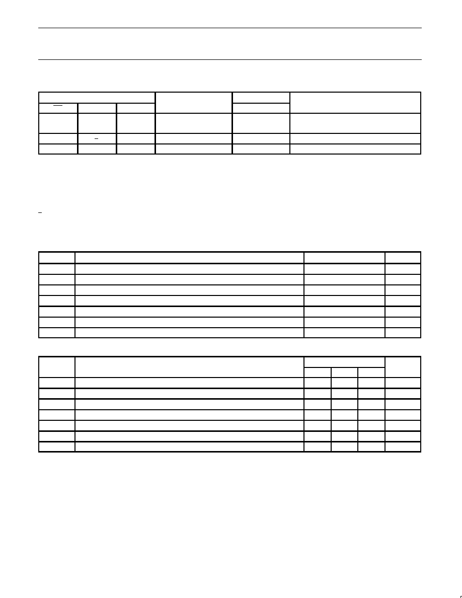
FUNCTION TABLE ≠ 74F574
INPUTS
INTERNAL
OUTPUTS
OPERATING MODES
OE
CP
Dn
REGISTER
Q0 ≠ Q7
OPERATING MODES
L
L
l
h
L
H
L
H
Load and read register
L
X
NC
NC
Hold
H
Dn
Dn
Z
Disable outputs
H = High voltage level
h = High voltage level one setup time prior to the Low-to-High clock transition
L = Low voltage level
l
= Low voltage level one setup time prior to the Low-to-High clock transition
NC= No change
X = Don't care
Z = High impedance "off" state
= Low-to-High clock transition
= Not a Low-to-High clock transition
ABSOLUTE MAXIMUM RATINGS
(Operation beyond the limits set forth in this table may impair the useful life of the device.
Unless otherwise noted these limits are over the operating free-air temperature range.)
SYMBOL
PARAMETER
RATING
UNIT
V
CC
Supply voltage
≠0.5 to +7.0
V
V
IN
Input voltage
≠0.5 to +7.0
V
I
IN
Input current
≠30 to +5.0
mA
V
OUT
Voltage applied to output in High output state
≠0.5 to +V
CC
V
I
OUT
Current applied to output in Low output state
48
mA
T
amb
Operating free-air temperature range
0 to +70
∞
C
T
stg
Storage temperature
≠65 to +150
∞
C
RECOMMENDED OPERATING CONDITIONS
SYMBOL
PARAMETER
LIMITS
UNIT
SYMBOL
PARAMETER
MIN
NOM
MAX
UNIT
V
CC
Supply voltage
4.5
5.0
5.5
V
V
IH
High-level input voltage
2.0
V
V
IL
Low-level input voltage
0.8
V
I
IK
Input clamp current
≠18
mA
I
OH
High-level output current
≠3
mA
I
OL
Low-level output current
24
mA
T
amb
Operating free-air temperature range
0
70
∞
C