 | –≠–ª–µ–∫—Ç—Ä–æ–Ω–Ω—ã–π –∫–æ–º–ø–æ–Ω–µ–Ω—Ç: N74F583D | –°–∫–∞—á–∞—Ç—å:  PDF PDF  ZIP ZIP |

Philips
Semiconductors
74F583
4-bit BCD adder
Product specification
IC15 Data Handbook
1989 Apr 06
INTEGRATED CIRCUITS
Philips Semiconductors
Product specification
74F583
4-bit BCD adder
2
1989 Apr 06
853≠1245 96263
FEATURES
∑
Adds two decimal numbers
∑
Full internal look-ahead
∑
Fast ripple carry for economical expansion
∑
Sum output delay 19.5 ns max.
∑
Ripple carry delay 8.5 ns max.
∑
Input to ripple delay 13.0 ns max.
∑
Supply current 60 mA max.
DESCRIPTION
The 74F583 4-bit coded (BCD) full adder performs the addition of
two decimal numbers (A0≠A3, B0≠B3). The look-ahead generates
BCD carry terms internally, allowing the 74F583 to then do BCD
addition correctly. For BCD numbers 0 through 9 at A and B inputs,
the BCD sum forms at the output.
In addition of two BCD numbers totalling a number greater than 9, a
valid BCD number and carry will result. For input values larger than
9, the number is converted from binary to BCD. Binary to BCD
conversion occurs by grounding one set of inputs, An or Bn, and
applying a 4-bit binary number to the other set of inputs. If the input
is between 0 and 9, a BCD number occurs at the output. If the
binary input falls between 10 and 15, a carry term is generated. Both
the carry term and the sum are the BCD equivalent of the binary
input. Converting binary numbers greater than 16 may be achieved
by cascading 74F583s.
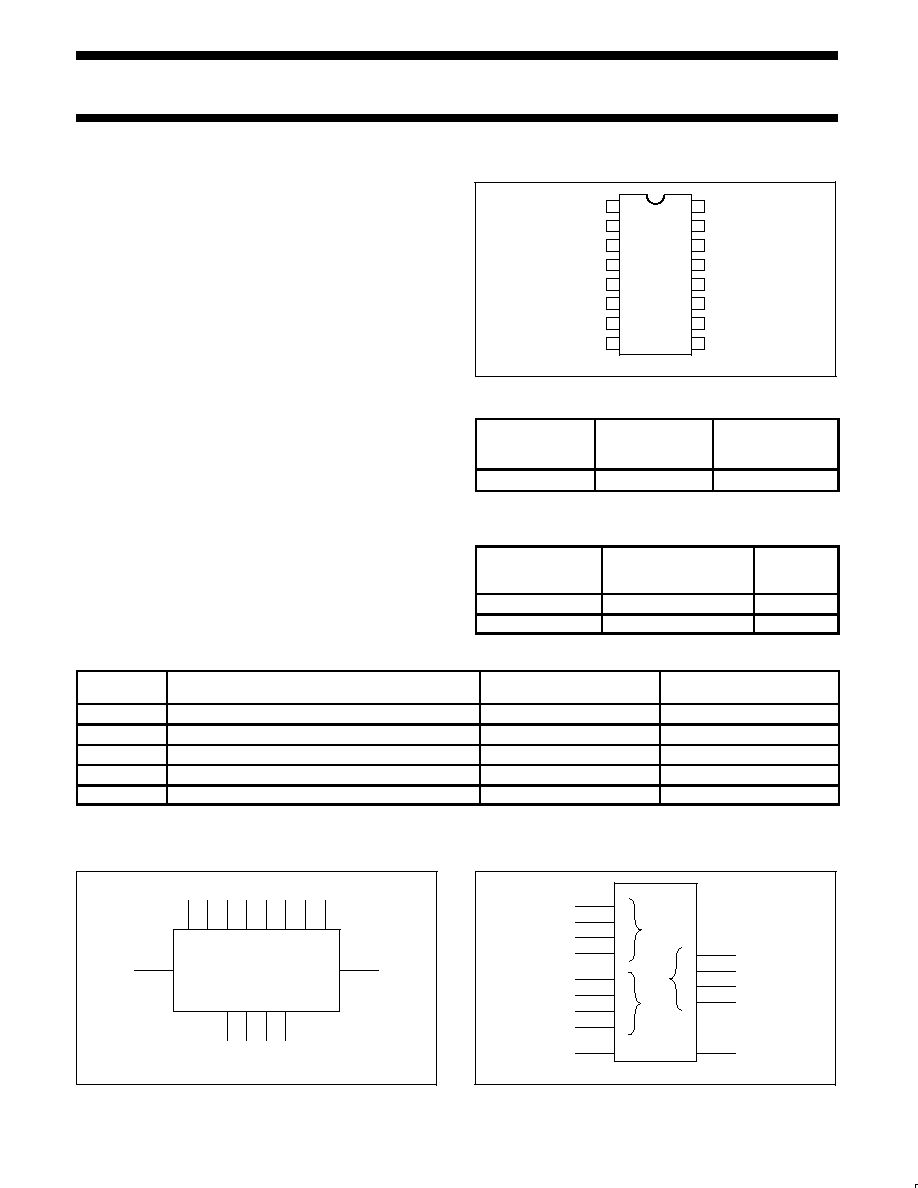
PIN CONFIGURATION
1
2
3
4
5
6
7
8
9
10
11
12
13
14
15
16
B1
B2
B3
A3
C
n
C
n+4
S2
GND
V
CC
A2
A1
A0
B0
S0
S1
S3
SF01436
TYPE
TYPICAL
PROPAGATION
DELAY
TYPICAL
SUPPLY CURRENT
(TOTAL)
74F583
9.0 ns
45 mA
ORDERING INFORMATION
PACKAGE
COMMERCIAL RANGE
V
CC
= 5 V
±
10%
T
amb
= 0
∞
C to +70
∞
C
DRAWING
NUMBER
16-pin plastic DIP
N74F583N
SOT38-4
16-pin plastic SO
N74F583D
SOT109-1
INPUT AND OUTPUT LOADING AND FAN-OUT TABLE
PINS
DESCRIPTION
74F (U.L.)
HIGH / LOW
LOAD VALUE
HIGH / LOW
A0≠A3
A operand inputs
1.0 / 2.0
20
µ
A / 1.2 mA
B0≠B3
B operand inputs
1.0 / 2.0
20
µ
A / 1.2 mA
C
n
Carry input
1.0 / 1.0
20
µ
A / 0.6 mA
C
n+4
Carry output
50 / 33
1.0 mA / 20 mA
S0≠S3
Sum outputs
50 / 33
1.0 mA / 20 mA
NOTE:
One (1.0) FAST Unit Load is defined as 20
µ
A in the High state and 0.6 mA in the Low state.
LOGIC SYMBOL
A0
B0
A1
B1
A2
B2
A3
B3
S0
S1
S2
S3
3
4
2
15
1
14
12
13
11
10
7
9
C
n
C
n+4
6
5
V
CC
= Pin 16
GND = Pin 8
SF01437
LOGIC SYMBOL (IEEE/IEC)
13
14
15
4
12
1
2
3
5
11
10
7
9
6
0
3
CO
CI
0
3
0
3
P
Q
(BCD)
SF01438
Philips Semiconductors
Product specification
74F583
4-bit BCD adder
1989 Apr 06
3
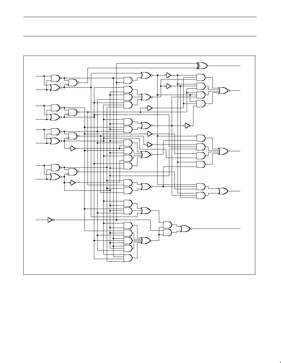
LOGIC DIAGRAM
11
10
7
9
6
S0
S1
S2
S3
C
n+4
B0
A0
B1
A1
B2
A2
B3
A3
C
n
12
13
1
14
2
15
3
4
5
V
CC
= PIN 16
GND = PIN 8
SF01435
Philips Semiconductors
Product specification
74F583
4-bit BCD adder
1989 Apr 06
4
ABSOLUTE MAXIMUM RATINGS
Operation beyond the limits set forth in this table may impair the useful life of the device.
Unless otherwise noted, these limits are over the operating free-air temperature range.
SYMBOL
PARAMETER
RATING
UNIT
V
CC
Supply voltage
≠0.5 to +7.0
V
V
IN
Input voltage
≠0.5 to +7.0
V
I
IN
Input current
≠30 to +5
mA
V
OUT
Voltage applied to output in High output state
≠0.5 to +V
CC
V
I
OUT
Current applied to output in Low output state
40
mA
T
amb
Operating free-air temperature range
0 to +70
∞
C
T
stg
Storage temperature range
≠65 to +150
∞
C
RECOMMENDED OPERATING CONDITIONS
SYMBOL
PARAMETER
LIMITS
UNIT
SYMBOL
PARAMETER
MIN
NOM
MAX
UNIT
V
CC
Supply voltage
4.5
5.0
5.5
V
V
IH
High-level input voltage
2.0
V
V
IL
Low-level input voltage
0.8
V
I
IK
Input clamp current
≠18
mA
I
OH
High-level output current
≠1
mA
I
OL
Low-level output current
20
mA
T
amb
Operating free-air temperature range
0
70
∞
C
DC ELECTRICAL CHARACTERISTICS
Over recommended operating free-air temperature range unless otherwise noted.
SYMBOL
PARAMETER
TEST CONDITIONS
1
LIMITS
UNIT
SYMBOL
PARAMETER
TEST CONDITIONS
1
MIN
TYP
2
MAX
UNIT
V
O
High level output voltage
V
CC
= MIN, V
IL
= MAX
±
10% V
CC
2.5
V
V
OH
High-level output voltage
V
IH
= MIN, I
OH
= MAX
±
5% V
CC
2.7
3.4
V
V
O
Low level output voltage
V
CC
= MIN, V
IL
= MAX
±
10% V
CC
0.30
0.50
V
V
OL
Low-level output voltage
V
IH
= MIN, I
OL
= MAX
±
5% V
CC
0.30
0.50
V
V
IK
Input clamp voltage
V
CC
= MIN, I
I
= I
IK
≠0.73
≠1.2
V
I
I
Input current at maximum input voltage
V
CC
= MAX, V
I
= 7.0 V
100
µ
A
I
IH
High-level input current
V
CC
= MAX, V
I
= 2.7 V
20
µ
A
I
Low level input current
C
n
only
V
CC
= MAX, V
I
= 0.5 V
≠0.6
mA
I
IL
Low-level input current
A
n
and B
n
V
CC
= MAX, V
I
= 0.5 V
≠1.2
mA
I
OS
Short circuit output current
3
V
CC
= MAX
≠60
≠150
mA
I
CC
Supply current (total)
V
CC
= MAX
45
60
mA
NOTES:
1. For conditions shown as MIN or MAX, use the appropriate value specified under recommended operating conditions for the applicable type.
2. All typical values are at V
CC
= 5 V, T
amb
= 25
∞
C.
3. Not more than one output should be shorted at a time. For testing I
OS
, the use of high-speed test apparatus and/or sample-and-hold
techniques are preferable in order to minimize internal heating and more accurately reflect operational values. Otherwise, prolonged shorting
of a High output may raise the chip temperature well above normal and thereby cause invalid readings in other parameter tests. In any
sequence of parameter tests, I
OS
tests should be performed last.
Philips Semiconductors
Product specification
74F583
4-bit BCD adder
1989 Apr 06
5
AC ELECTRICAL CHARACTERISTICS
LIMITS
SYMBOL
PARAMETER
TEST CONDITION
T
amb
= +25
∞
C
V
CC
= 5 V
C
L
= 50 pF; R
L
= 500
T
amb
= 0
∞
C to +70
∞
C
V
CC
= 5 V
±
10%
C
L
= 50 pF; R
L
= 500
UNIT
MIN
TYP
MAX
MIN
MAX
t
PLH
t
PHL
Propagation delay
An or Bn to Sn
Waveform 1
5.0
5.0
13.0
10.5
17.0
14.0
5.0
5.0
18.0
15.0
ns
t
PLH
t
PHL
Propagation delay
An or Bn to Sn (INV)
Waveform 2
6.0
4.0
11.0
8.0
18.0
12.0
5.0
4.0
19.5
12.5
ns
t
PLH
t
PHL
Propagation delay
C
n
to C
n+4
Waveform 1, 2
3.5
2.5
5.0
4.0
8.0
7.0
3.0
2.0
8.5
7.0
ns
t
PLH
t
PHL
Propagation delay
An or Bn to C
n+4
Waveform 1, 2
5.0
5.0
8.0
7.5
11.5
10.5
4.5
4.5
13.0
11.5
ns
t
PLH
t
PHL
Propagation delay
C
n
to Sn
Waveform 1
4.0
3.5
12.0
8.0
15.5
12.5
3.5
3.0
17.0
13.5
ns
t
PLH
t
PHL
Propagation delay
C
n
to Sn (INV)
Waveform 2
6.0
3.5
9.5
8.0
13.0
11.5
5.0
3.0
14.5
12.0
ns
AC WAVEFORMS
For all waveforms, V
M
= 1.5 V.
An, Bn, C
n
Sn, C
n+4
V
M
V
M
V
M
V
M
t
PLH
t
PHL
SF01439
Waveform 1.
Propagation delay for non-inverting outputs
An, Bn, C
n
Sn, C
n+4
V
M
V
M
V
M
V
M
t
PHL
t
PLH
SF01440
Waveform 2.
Propagation delay for inverting outputs
TEST CIRCUIT AND WAVEFORMS
tw
90%
VM
10%
90%
VM
10%
90%
VM
10%
90%
VM
10%
NEGATIVE
PULSE
POSITIVE
PULSE
tw
AMP (V)
0V
0V
tTHL (tf
)
INPUT PULSE REQUIREMENTS
rep. rate
t
w
t
TLH
t
THL
1MHz
500ns
2.5ns
2.5ns
Input Pulse Definition
VCC
family
74F
D.U.T.
PULSE
GENERATOR
RL
CL
RT
VIN
VOUT
Test Circuit for Totem-Pole Outputs
DEFINITIONS:
R
L
= Load resistor;
see AC ELECTRICAL CHARACTERISTICS for value.
C
L
= Load capacitance includes jig and probe capacitance;
see AC ELECTRICAL CHARACTERISTICS for value.
R
T
= Termination resistance should be equal to Z
OUT
of
pulse generators.
tTHL (tf
)
tTLH (tr
)
tTLH (tr
)
AMP (V)
amplitude
3.0V
1.5V
V
M
SF00006
Philips Semiconductors
Product specification
74F583
4-bit BCD adder
1989 Apr 06
6
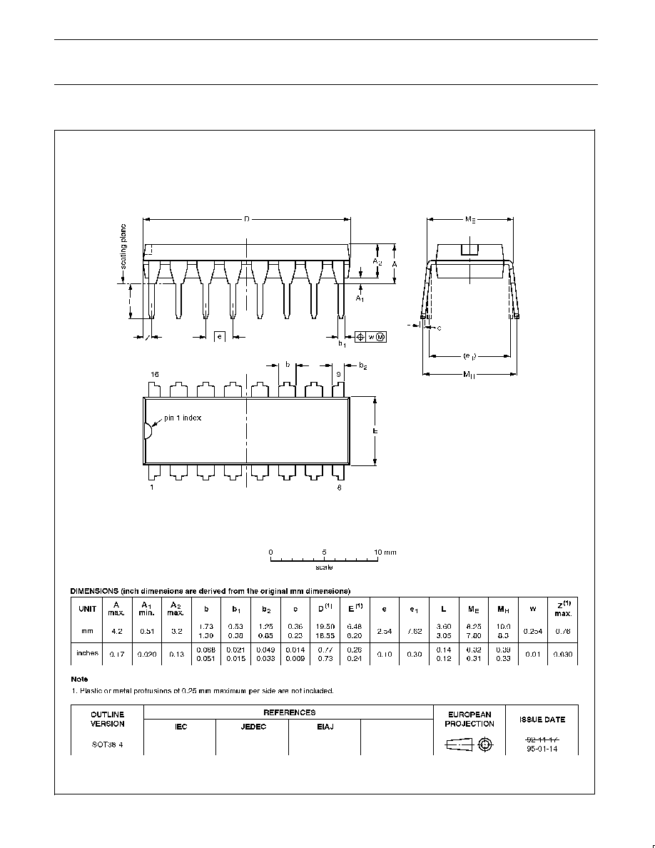
DIP16:
plastic dual in-line package; 16 leads (300 mil)
SOT38-4
Philips Semiconductors
Product specification
74F583
4-bit BCD adder
1989 Apr 06
7
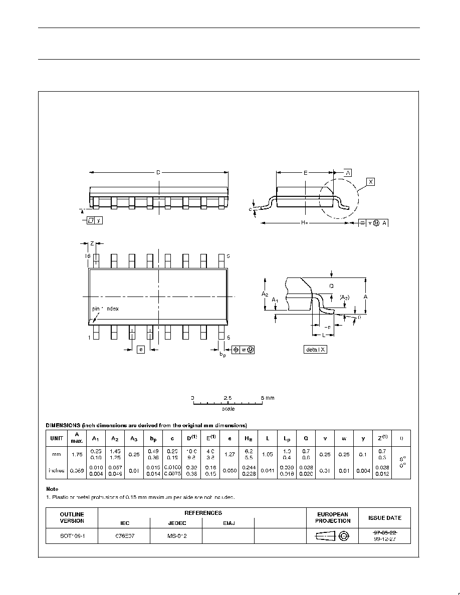
SO16:
plastic small outline package; 16 leads; body width 3.9 mm
SOT109-1
Philips Semiconductors
Product specification
74F583
4-bit BCD adder
1989 Apr 06
8
Definitions
Short-form specification -- The data in a short-form specification is extracted from a full data sheet with the same type number and title. For
detailed information see the relevant data sheet or data handbook.
Limiting values definition -- Limiting values given are in accordance with the Absolute Maximum Rating System (IEC 134). Stress above one
or more of the limiting values may cause permanent damage to the device. These are stress ratings only and operation of the device at these or
at any other conditions above those given in the Characteristics sections of the specification is not implied. Exposure to limiting values for extended
periods may affect device reliability.
Application information -- Applications that are described herein for any of these products are for illustrative purposes only. Philips
Semiconductors make no representation or warranty that such applications will be suitable for the specified use without further testing or
modification.
Disclaimers
Life support -- These products are not designed for use in life support appliances, devices or systems where malfunction of these products can
reasonably be expected to result in personal injury. Philips Semiconductors customers using or selling these products for use in such applications
do so at their own risk and agree to fully indemnify Philips Semiconductors for any damages resulting from such application.
Right to make changes -- Philips Semiconductors reserves the right to make changes, without notice, in the products, including circuits, standard
cells, and/or software, described or contained herein in order to improve design and/or performance. Philips Semiconductors assumes no
responsibility or liability for the use of any of these products, conveys no license or title under any patent, copyright, or mask work right to these
products, and makes no representations or warranties that these products are free from patent, copyright, or mask work right infringement, unless
otherwise specified.
Philips Semiconductors
811 East Arques Avenue
P.O. Box 3409
Sunnyvale, California 94088≠3409
Telephone 800-234-7381
©
Copyright Philips Electronics North America Corporation 1989
All rights reserved. Printed in U.S.A.
Date of release: 04-00
Document order number:
9397 750 07093
Philips
Semiconductors
Data sheet
status
Objective
specification
Preliminary
specification
Product
specification
Product
status
Development
Qualification
Production
Definition
[1]
This data sheet contains the design target or goal specifications for product development.
Specification may change in any manner without notice.
This data sheet contains preliminary data, and supplementary data will be published at a later date.
Philips Semiconductors reserves the right to make changes at any time without notice in order to
improve design and supply the best possible product.
This data sheet contains final specifications. Philips Semiconductors reserves the right to make
changes at any time without notice in order to improve design and supply the best possible product.
Data sheet status
[1]
Please consult the most recently issued datasheet before initiating or completing a design.