 | –≠–ª–µ–∫—Ç—Ä–æ–Ω–Ω—ã–π –∫–æ–º–ø–æ–Ω–µ–Ω—Ç: N74F598N | –°–∫–∞—á–∞—Ç—å:  PDF PDF  ZIP ZIP |

Philips
Semiconductors
74F598
8-bit shift register with input storage
registers (3-State)
Product specification
IC15 Data Handbook
1991 Oct 21
INTEGRATED CIRCUITS

Philips Semiconductors
Product specification
74F598
8-bit shift register with input storage registers (3-State)
2
1991 Oct 21
853≠1583 04407
FEATURES
∑
High impedance PNP base input for reduced loading (20
µ
A in
High and Low states)
∑
8≠bit parallel storage register
∑
Shift register has asynchronous direct overriding reset
∑
Shift load SHLD is functional when SHCP is Low and locked out
when SHCP is High.
∑
Guaranteed shift frequency DC to 105MHz
∑
Parallel 3≠State I/O storage register inputs and shift register
parallel outputs
DESCRIPTION
The 74F598 consists of an 8≠bit storage register feeding a
parallel≠in/serial≠in, parallel≠out/serial≠out 8≠bit shift register. Both
the storage register and shift register have positive edge≠triggered
clocks. The shift register has asynchronous reset and when SHCP
is Low, it has asynchronous load.
The shift register load function has been modified to load when both
SHLD and SHCP are Low. When SHCP is High the shift register
load operation is not performed. Data will be properly shifted on the
rising edge of SHCP when SHLD is High.
TYPE
TYPICAL SHCP f
max
TYPICAL SUPPLY
CURRENT (TOTAL)
74F598
100MHz
75mA
ORDERING INFORMATION
ORDER CODE
DESCRIPTION
COMMERCIAL RANGE
V
CC
= 5V
±
10%,
T
amb
= 0
∞
C to +70
∞
C
PKG DWG #
20≠pin plastic DIP
N74F598N
SOT146-1
20≠pin plastic SOL
N74F598D
SOT163-1
INPUT AND OUTPUT LOADING AND FAN OUT TABLE
PINS
DESCRIPTION
74F (U.L.) High/
Low
LOAD VALUE
High/Low
I/On
Parallel data input
1.0/0.033
20
µ
A/20
µ
A
Ds0, Ds1
Serial data inputs
1.0/0.033
20
µ
A/20
µ
A
SHCP
Shift register clock pulse input
1.0/0.033
20
µ
A/20
µ
A
STCP
Storage register clock pulse input
1.0/0.033
20
µ
A/20
µ
A
SHCPEN
Shift register clock pulse enable input
1.0/0.033
20
µ
A/20
µ
A
SHLD
Shift register load input (active Low)
1.0/0.033
20
µ
A/20
µ
A
SHRST
Shift register reset input (active Low)
1.0/0.033
20
µ
A/20
µ
A
S
Serial data select input
1.0/0.033
20
µ
A/20
µ
A
OE
Output enable input
1.0/0.033
20
µ
A/20
µ
A
Qs
Serial data output
50/33
1.0mA/20mA
I/On
Parallel data outputs
150/40
3.0mA/24mA
Note to input and output loading and fan out table
1. One (1.0) FAST unit load is defined as: 20
µ
A in the High state and 0.6mA in the Low state.
PIN CONFIGURATION
1
2
3
4
5
6
7
8
9
10
11
12
13
14
15
16
17
18
19
20 VCC
S
DS0
DS1
OE
STCP
SHCPEN
SHCP
SHRST
Qs
I/O0
I/O1
I/O2
I/O3
I/O4
I/O5
I/O6
I/O7
SHLD
GND
SF00375
LOGIC SYMBOL
Qs
V
CC
= Pin 20
GND = Pin 10
S
OE
STCP
SHCPEN
SHCP
SHRST
SHLD
19
16
15
14
13
12
9
11
Ds0
18
Ds1
17
I/O0
1
I/O1
2
I/O2
3
I/O3
4
I/O4
5
I/O5
6
I/O6
7
I/O7
8
SF00376

Philips Semiconductors
Product specification
74F598
8-bit shift register with input storage registers (3-State)
1991 Oct 21
3
IEC/IEEE SYMBOL
18
17
1
2
3
4
5
6
7
8
EN14
R
G4
16
12
14
13
9
15
19
1, 5D
1, 5D
2D
6, 14
2D
7, 14
2D
13, 14
SRG8
11
C2
4C5/4
C1
3D
3D
G1
3D
Z6
Z7
Z13
SF00377
FUNCTION TABLE
INPUTS
INPUTS/OUTPUTS
OPERATING MODE
SHRST
STCP
SHCP
SHLD
S
OE*
I/O0
I/O1
I/O2
I/O3
I/O4
I/O5
I/O6
I/O7
Q7
L
X
L
H
X
L
L
L
L
L
L
L
L
L
L
Clear shift register
L
X
L
L
X
L
Invalid, state of shift register in-
determinate when signal is re-
moved
X
X
X
X
H
I0
I1
I2
I3
I4
I5
I6
I7
O7
Load data to storage register
H
X
H
L
L
Ds0
O0
O1
O2
O3
O4
O5
O6
O6
Shift right
H
X
H
H
L
Ds1
O0
O1
O2
O3
O4
O5
O6
O6
H
L
L
X
H
I0
I1
I2
I3
I4
I5
I6
I7
O7
Load data directly to shift regis-
ter
H
L
L
X
X
O0
O1
O2
O3
O4
O5
O6
O7
O7
Data transferred from storage
register to shift register
X
X
X
X
X
H
Z
Z
Z
Z
Z
Z
Z
Z
NC
3≠State
H
X
H
X
X
NC
NC
NC
NC
NC
NC
NC
NC
NC
Hold
H
H
X
X
X
NC
NC
NC
NC
NC
NC
NC
NC
NC
Hold (no storage or shift register
load
Notes to function table
D0 ≠ D7 = The level of the steady state inputs to the serial multiplexer.
H = High voltage level
I0 ≠ I7 = The level of the steady state input at the respective I/O terminal is loaded into the flip≠flop while the flip≠flop outputs ( except Q7) are isolated
from the I/O terminal.
L
= Low voltage level
NC= No change
O0 ≠ O7 = The level of the respective Qn flip≠flop prior to the last clock Low≠to≠High transition
X = Don't care
Z = High impedance "off" state
*
= When the OE input is High, all I/O terminals are at the High impedance state, sequential operation or cleaning of the register is not affected.
= Low≠to≠High clock transition
= Not Low≠to≠High clock transition
Philips Semiconductors
Product specification
74F598
8-bit shift register with input storage registers (3-State)
1991 Oct 21
4
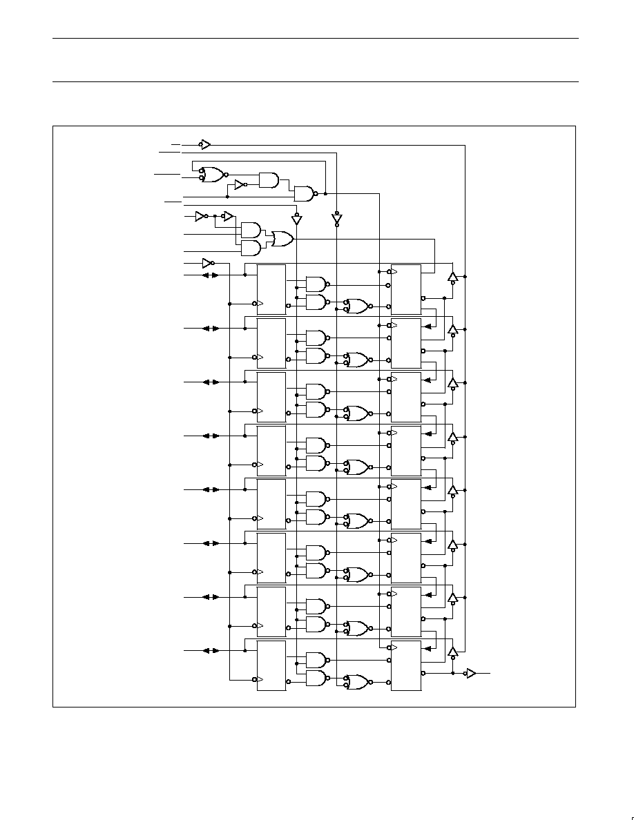
LOGIC DIAGRAM
V
CC
= Pin 20
GND = Pin 10
C2
2D
S
R
1D
C1
I/O0
I/O1
I/O2
I/O3
I/O4
I/O5
I/O6
I/O7
1
2
3
4
5
6
7
8
C2 3S
3R
S
R
1D
C1
C2
S
R
1D
C1
C2
S
R
1D
C1
C2
S
R
1D
C1
C2
S
R
1D
C1
C2
S
R
1D
C1
C2
S
R
1D
C1
9
Qs
17
15
Ds1
STCP
16
12
OE
SHRST
14
SHCPEN
13
9
SHCP
SHLD
19
18
S
Ds0
3S
3R
3S
3R
3S
3R
3S
3R
3S
3R
3S
3R
SF00378

Philips Semiconductors
Product specification
74F598
8-bit shift register with input storage registers (3-State)
1991 Oct 21
5
ABSOLUTE MAXIMUM RATINGS
(Operation beyond the limit set forth in this table may impair the useful life of the device. Unless otherwise noted these limits are over the
operating free air temperature range.)
SYMBOL
PARAMETER
RATING
UNIT
V
CC
Supply voltage
≠0.5 to +7.0
V
V
IN
Input voltage
≠0.5 to +7.0
V
I
IN
Input current
≠30 to +5
mA
V
OUT
Voltage applied to output in High output state
≠0.5 to V
CC
V
I
OUT
Current applied to output in Low output state
Qs
40
mA
I/O0 ≠ I/O7
48
mA
T
amb
Operating free air temperature range
0 to +70
∞
C
T
stg
Storage temperature range
≠65 to +150
∞
C
RECOMMENDED OPERATING CONDITIONS
SYMBOL
PARAMETER
LIMITS
UNIT
MIN
NOM
MAX
V
CC
Supply voltage
4.5
5.0
5.5
V
V
IH
High≠level input voltage
2.0
V
V
IL
Low≠level input voltage
0.8
V
I
Ik
Input clamp current
≠18
mA
I
OH
High≠level output current
Qs
≠1
mA
I/O0 ≠ I/O7
≠3
mA
I
OL
Low≠level output current
Qs
20
mA
I/O0 ≠ I/O7
24
mA
T
amb
Operating free air temperature range
0
+70
∞
C

Philips Semiconductors
Product specification
74F598
8-bit shift register with input storage registers (3-State)
1991 Oct 21
6
DC ELECTRICAL CHARACTERISTICS
(Over recommended operating free-air temperature range unless otherwise noted.)
SYMBOL
PARAMETER
TEST
LIMITS
UNIT
CONDITIONS
1
MIN
TYP
2
MAX
Qs
V
CC
= MIN,
V
IL
= MAX,
I
OH
= ≠1mA
±
10%V
CC
2.5
V
V
OH
High-level output voltage
V
IL
= MAX,
±
5%V
CC
2.7
3.4
V
I/On
V
IH
= MIN,
V
IL
= MAX,
I
OH
= ≠3mA
±
10%V
CC
2.4
V
±
5%V
CC
2.7
3.3
V
V
OL
Low-level output voltage
V
CC
= MIN, V
IL
= MAX,
±
10%V
CC
0.30
0.50
V
V
IH
= MIN, I
OL
= MAX
±
5%V
CC
0.30
0.50
V
V
IK
Input clamp voltage
V
CC
= MIN, I
I
= I
IK
≠0.73
-1.2
V
I
I
Input current at maximum input voltage
others
V
CC
= MAX, V
I
= 7.0V
100
µ
A
I/On
V
CC
= MAX, V
I
= 5.5V
1
mA
I
IH
High≠level input current
V
CC
= MAX, V
I
= 2.7V
20
µ
A
I
IL
Low≠level input current
V
CC
= MAX, V
I
= 0.5V
≠20
µ
A
I
OZH
+ I
IH
Off≠state output current,
High≠level voltage applied
I/On
V
CC
= MAX, V
O
= 2.7V
70
µ
A
I
OZL
+ I
IL
Off≠state output current,
Low≠level voltage applied
only
V
CC
= MAX, V
O
= 0.5V
≠70
µ
A
I
OS
Short≠circuit output current
3
V
CC
= MAX
-60
-150
mA
I
CCH
68
100
mA
I
CC
Supply current (total)
I
CCL
V
CC
= MAX
80
110
mA
I
CCZ
73
105
mA
Notes to DC electrical characteristics
1. For conditions shown as MIN or MAX, use the appropriate value specified under recommended operating conditions for the applicable type.
2. All typical values are at V
CC
= 5V, T
amb
= 25
∞
C.
3. Not more than one output should be shorted at a time. For testing I
OS
, the use of High-speed test apparatus and/or sample-and-hold
techniques are preferable in order to minimize internal heating and more accurately reflect operational values. Otherwise, prolonged shorting
of a High output may raise the chip temperature well above normal and thereby cause invalid readings in other parameter tests. In any
sequence of parameter tests, I
OS
tests should be performed last.

Philips Semiconductors
Product specification
74F598
8-bit shift register with input storage registers (3-State)
1991 Oct 21
7
AC ELECTRICAL CHARACTERISTICS
LIMITS
T
amb
= +25
∞
C
T
amb
= 0
∞
C to +70
∞
C
SYMBOL
PARAMETER
TEST
V
CC
= +5.0V
V
CC
= +5.0V
±
10%
UNIT
CONDITION
C
L
= 50pF, R
L
= 500
C
L
= 50pF, R
L
= 500
MIN
TYP
MAX
MIN
MAX
f
max
Maximum clock frequency
SHCP
Waveform 1
85
100
70
MHz
STCP
140
160
130
t
PLH
t
PHL
Propagation delay
SHCP to Qs
Waveform 1
9.5
6.5
11.5
8.5
14.0
11.5
8.5
6.0
16.0
12.0
ns
t
PLH
t
PHL
Propagation delay
STCP to Qs (SHLD = Low)
Waveform 1
10.0
7.0
11.5
8.5
14.5
11.5
9.0
6.5
16.0
12.5
ns
t
PLH
t
PHL
Propagation delay
SHLD to Qs
Waveform 1
9.0
6.0
11.0
8.0
13.5
10.5
8.0
5.5
15.5
11.5
ns
t
PLH
t
PHL
Propagation delay
SHCP to I/On
Waveform 1
8.5
5.0
10.5
7.0
13.5
9.5
7.0
4.5
15.5
10.5
ns
t
PLH
t
PHL
Propagation delay
SHLD to I/On
Waveform 1
7.5
6.0
9.5
8.0
12.5
11.0
6.5
6.0
14.5
11.5
ns
t
PHL
Propagation delay, SHRST to I/On
Waveform 2
6.5
9.0
12.0
6.0
12.5
ns
t
PHL
Propagation delay, SHRST to Qs
Waveform 2
6.0
7.5
10.5
5.0
11.0
ns
t
PZH
t
PZL
Output enable time to
High or Low
Waveform 5
Waveform 6
3.5
3.0
5.5
5.0
8.5
7.5
3.0
2.5
9.5
8.5
ns
t
PHZ
t
PLZ
Output disable time to
High or Low
Waveform 5
Waveform 6
1.5
4.0
3.5
6.0
6.5
9.0
1.5
4.0
7.5
9.5
ns

Philips Semiconductors
Product specification
74F598
8-bit shift register with input storage registers (3-State)
1991 Oct 21
8
AC SETUP REQUIREMENTS
LIMITS
T
amb
= +25
∞
C
T
amb
= 0
∞
C to +70
∞
C
SYMBOL
PARAMETER
TEST
V
CC
= +5.0V
V
CC
= +5.0V
±
10%
UNIT
CONDITION
C
L
= 50pF, R
L
= 500
C
L
= 50pF, R
L
= 500
MIN
TYP
MAX
MIN
MAX
t
s
(H)
t
s
(L)
Setup time, High or Low
Dsn to SHCP
Waveform 3
0.0
3.5
1.5
4.5
ns
t
h
(H)
t
h
(L)
Hold time, High or Low
DSn to SHCP
Waveform 3
0.0
2.5
0.0
3.0
ns
t
s
(H)
t
s
(L)
Setup time, High or Low
I/On to STCP
Waveform 3
2.5
2.5
2.5
3.0
ns
t
h
(H)
t
h
(L)
Hold time, High or Low
I/On to STCP
Waveform 3
0.0
0.0
1.5
2.0
ns
t
s
(H)
t
s
(L)
Setup time, High or Low
S to SHCP
Waveform 3
3.5
3.0
4.0
3.5
ns
t
h
(H)
t
h
(L)
Hold time, High or Low
S to SHCP
Waveform 3
2.5
3.0
3.0
3.0
ns
t
s
(H)
Setup time, High, STCP to SHLD
Waveform 4
7.0
8.0
ns
t
h
(L)
Hold time, Low, STCP to SHLD (hold mode)
Waveform 4
0.0
0.0
ns
t
s
(H)
t
s
(L)
Setup time, High or Low, SHCPEN to SHCP
Waveform 3
0.0
2.0
0.0
2.0
ns
t
h
(H)
t
h
(L)
Hold time, High or Low, SHCPEN to SHCP
Waveform 3
0.0
4.5
0.0
5.5
ns
t
s
(H)
Setup time, High, SHLD to SHCP
Waveform 3
7.5
8.5
ns
t
w
(H)
t
w
(L)
SHCP Pulse width,
High or Low
Waveform 1
5.5
4.0
6.5
4.0
ns
t
w
(H)
t
w
(L)
STCP Pulse width,
High or Low
Waveform 1
4.5
4.0
5.5
4.0
ns
t
w
(L)
SHRST Pulse width, Low
Waveform 1
4.0
4.0
ns
t
w
(L)
SHLD Pulse width, Low
Waveform 1
4.0
5.0
ns
t
rec
Recovery time, SHRST to SHCP
Waveform 2
0.0
0.0
ns

Philips Semiconductors
Product specification
74F598
8-bit shift register with input storage registers (3-State)
1991 Oct 21
9
TYPICAL TIMING DIAGRAM
OE
SHRST
SHLD
SHCP
SHCPEN
STCP
S
Ds0
Ds1
I/O0
I/O1
I/O2
I/O3
I/O4
I/O5
I/O6
I/O7
Qs
output
Hi≠Z
input Hi≠Z
shift and output
Don't care
Don't care
Don't care
Don't care
Don't care
Don't care
SF00379

Philips Semiconductors
Product specification
74F598
8-bit shift register with input storage registers (3-State)
1991 Oct 21
10
AC WAVEFORMS
VM
VM
VM
tw(H)
1/fmax
VM
VM
tPLH
tw(L)
tPHL
I/On,
Qs
STCP,
SHCP,
SHLD,
SHRST
SF00380
Waveform 1. Propagation delay for clock input to output, clock
pulse widths, and maximum clock frequency, shift register
reset and load inputs to serial data output
SHRST
VM
VM
VM
SHCP
trec
VM
I/On,
Qs
tPHL
SF00381
Waveform 2. Propagation delay for shift register reset to serial
data output, shift register reset to shift register, shift register
input recovery time
VM
VM
VM
VM
VM
VM
ts(L)
th(L)
ts(H)
th(H)
Dsn, I/On,
SHCP,
SHLD,
SHCPEN
SHCP,
STCP
SHLD
SF00382
Waveform 3. Setup time and hold times
VM
VM
STCP
SHLD
ts(H)
VM
th(L)
SF00383
Waveform 4. Setup time and hold time
VM
VM
VM
tPHZ
tPZH
OE
I/On
VOH -0.3V
0V
10%
90%
SF00384
Waveform 5. 3-State output enable time to High level, output
disable time from High level and transition time to High level
VM
VM
VM
tPLZ
tPZL
VOL +0.3V
3.5V
10%
90%
OE
I/On
SF00385
Waveform 6. 3-State output enable time to Low level, output
disable time from Low level and transition time to Low level
Notes to AC waveforms
1. For all waveforms, V
M
= 1.5V.
2. The shaded areas indicate when the input is permitted to change for predictable output performance.

Philips Semiconductors
Product specification
74F598
8-bit shift register with input storage registers (3-State)
1991 Oct 21
11
TEST CIRCUIT AND WAVEFORMS
tw
90%
VM
10%
90%
VM
10%
90%
VM
10%
90%
VM
10%
NEGATIVE
PULSE
POSITIVE
PULSE
tw
AMP (V)
0V
0V
tTHL (tf
)
INPUT PULSE REQUIREMENTS
rep. rate
t
w
t
TLH
t
THL
1MHz
500ns
2.5ns
2.5ns
Input Pulse Definition
VCC
family
74F
D.U.T.
PULSE
GENERATOR
RL
CL
RT
VIN
VOUT
Test Circuit for Open Collector Outputs
DEFINITIONS:
R
L
= Load resistor;
see AC electrical characteristics for value.
C
L
= Load capacitance includes jig and probe capacitance;
see AC electrical characteristics for value.
R
T
= Termination resistance should be equal to Z
OUT
of
pulse generators.
tTHL (tf
)
tTLH (tr
)
tTLH (tr
)
AMP (V)
amplitude
3.0V
1.5V
V
M
RL
7.0V
SF00128
TEST
SWITCH
t
PLZ
closed
t
PZL
closed
All other
open
SWITCH POSITION

Philips Semiconductors
Product specification
74F598
8-bit shift register with input storage registers (3-State)
1991 Oct 21
12
DIP20:
plastic dual in-line package; 20 leads (300 mil)
SOT146-1

Philips Semiconductors
Product specification
74F598
8-bit shift register with input storage registers (3-State)
1991 Oct 21
13
SO20:
plastic small outline package; 20 leads; body width 7.5 mm
SOT163-1

Philips Semiconductors
Product specification
74F598
8-bit shift register with input storage registers (3-State)
yyyy mmm dd
14
Definitions
Short-form specification -- The data in a short-form specification is extracted from a full data sheet with the same type number and title. For
detailed information see the relevant data sheet or data handbook.
Limiting values definition -- Limiting values given are in accordance with the Absolute Maximum Rating System (IEC 134). Stress above one
or more of the limiting values may cause permanent damage to the device. These are stress ratings only and operation of the device at these or
at any other conditions above those given in the Characteristics sections of the specification is not implied. Exposure to limiting values for extended
periods may affect device reliability.
Application information -- Applications that are described herein for any of these products are for illustrative purposes only. Philips
Semiconductors make no representation or warranty that such applications will be suitable for the specified use without further testing or
modification.
Disclaimers
Life support -- These products are not designed for use in life support appliances, devices or systems where malfunction of these products can
reasonably be expected to result in personal injury. Philips Semiconductors customers using or selling these products for use in such applications
do so at their own risk and agree to fully indemnify Philips Semiconductors for any damages resulting from such application.
Right to make changes -- Philips Semiconductors reserves the right to make changes, without notice, in the products, including circuits, standard
cells, and/or software, described or contained herein in order to improve design and/or performance. Philips Semiconductors assumes no
responsibility or liability for the use of any of these products, conveys no license or title under any patent, copyright, or mask work right to these
products, and makes no representations or warranties that these products are free from patent, copyright, or mask work right infringement, unless
otherwise specified.
Philips Semiconductors
811 East Arques Avenue
P.O. Box 3409
Sunnyvale, California 94088≠3409
Telephone 800-234-7381
©
Copyright Philips Electronics North America Corporation 1998
All rights reserved. Printed in U.S.A.
print code
Date of release: 10-98
Document order number:
9397-750-05145
Philips
Semiconductors
Data sheet
status
Objective
specification
Preliminary
specification
Product
specification
Product
status
Development
Qualification
Production
Definition
[1]
This data sheet contains the design target or goal specifications for product development.
Specification may change in any manner without notice.
This data sheet contains preliminary data, and supplementary data will be published at a later date.
Philips Semiconductors reserves the right to make chages at any time without notice in order to
improve design and supply the best possible product.
This data sheet contains final specifications. Philips Semiconductors reserves the right to make
changes at any time without notice in order to improve design and supply the best possible product.
Data sheet status
[1]
Please consult the most recently issued datasheet before initiating or completing a design.