 | –≠–ª–µ–∫—Ç—Ä–æ–Ω–Ω—ã–π –∫–æ–º–ø–æ–Ω–µ–Ω—Ç: N74F621D | –°–∫–∞—á–∞—Ç—å:  PDF PDF  ZIP ZIP |

Philips
Semiconductors
74F621
Octal bus transceiver, non-inverting
(open collector)
Product specification
1996 Jan 05
INTEGRATED CIRCUITS
IC15 Data Handbook

Philips Semiconductors
Product specification
74F621
Octal bus transceiver, non-inverting (open collector)
2
1996 Jan 05
853≠0380 16185
FEATURES
∑
High-impedance NPN base inputs for reduced loading
(20
µ
A in High and Low states)
∑
Octal bidirectional bus interface
∑
Open collector outputs sink 64mA
∑
Non-inverting
DESCRIPTION
The 74F621 is an octal transceiver featuring non-inverting open
collector bus-compatible outputs in both send and receive
directions. The outputs are capable of sinking 64mA, providing very
good capacitive drive characteristics.
This octal bus transceiver is designed for asynchronous two-way
communication between data buses. The control function
implementation allows for maximum flexibility in timing.
The device allows data transmission from the A bus to the B bus or
from the B bus to the A bus, depending upon the logic levels at the
Enable inputs (OEBA and OEAB). The Enable inputs can be used to
disable the device so that the buses are effectively isolated.
The dual-enable configuration gives the 74F621 the capability to
store data by the simultaneous enabling of OEBA and OEAB. Each
output reinforces its input in this transceiver configuration. Thus,
when both control inputs are enabled and all other data sources to
the two sets of the bus lines are at high impedance, both sets of bus
lines (16 in all) will remain in their last states.
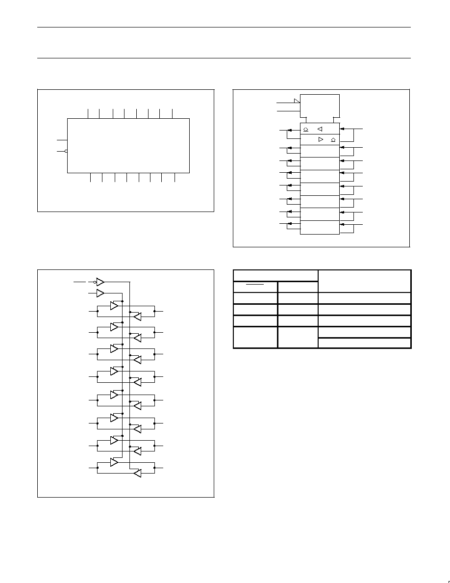
PIN CONFIGURATION
20
19
18
17
16
15
14
13
12
10
11
9
8
7
6
5
4
3
2
1
VCC
B1
B2
B3
B4
B5
B6
B7
OEAB
A1
A2
A3
A4
A5
A6
A7
GND
OEBA
A0
B0
SF01135
TYPE
TYPICAL
PROPAGATION
DELAY
TYPICAL SUPPLY CURRENT
(TOTAL)
74F621
8.0ns
105mA
ORDERING INFORMATION
DESCRIPTION
COMMERCIAL RANGE
V
CC
= 5V
±
10%,
T
amb
= 0
∞
C to +70
∞
C
PKG
DWG #
20-pin plastic DIP
N74F621N
SOT146-1
20-pin plastic SOL
N74F621D
SOT163-1
INPUT AND OUTPUT LOADING AND FAN-OUT TABLE
PINS
DESCRIPTION
74F(U.L.)
HIGH/LOW
LOAD VALUE
HIGH/LOW
A0 - A7, B0 - B7
Data inputs
1.0/0.033
20
µ
A/20
µ
A
OEBA, OEAB
Output Enable inputs
1.0/0.033
20
µ
A/20
µ
A
A0 - A7
Data outputs
OC/40
OC/24mA
B0 - B7
Data outputs
OC/106.7
OC/64mA
NOTE: One (1.0) FAST unit load is defined as: 20
µ
A in the High state and 0.6mA in the Low state. OC = Open Collector.
Philips Semiconductors
Product specification
74F621
Octal bus transceiver, non-inverting (open collector)
1996 Jan 05
3
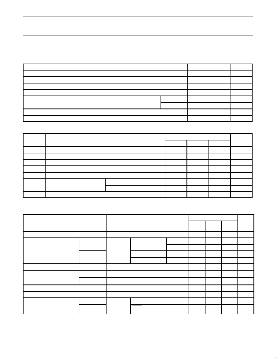
LOGIC SYMBOL
B0
B1
B2
B3
19
1
OEAB
OEBA
SF01126
V
CC
= Pin 20
GND = Pin 10
B4
B5
B6
B7
8
9
A2
A3
4
5
6
A4
A5
A6
7
A7
2
3
A0
A1
18
17
16
15
14
13
12
11
LOGIC SYMBOL (IEEE/IEC)
SF01137
19
18
EN1
1
17
16
15
14
13
12
11
2
3
4
5
6
7
8
9
2
1
EN2
LOGIC DIAGRAM
VCC =
Pin 20
GND =
Pin 10
SF01130
OEBA
2
3
4
18
17
16
15
14
13
12
B0
B1
B4
B5
B6
B7
OEAB
A1
A4
A5
A6
A7
B2
B3
A3
A2
5
6
7
8
A0
11
9
19
1
FUNCTION TABLE
INPUTS
OPERATING MODES
OEBA
OEAB
OPERATING MODES
L
L
B data to A bus
H
H
A data to B bus
H
L
OFF
L
H
B data to A bus
L
H
A data to B bus
H = High voltage level
L
= Low voltage level
X = Don't care
OFF= High if pull-up resistor is connected to open collector output
Philips Semiconductors
Product specification
74F621
Octal bus transceiver, non-inverting (open collector)
1996 Jan 05
4
ABSOLUTE MAXIMUM RATINGS
(Operation beyond the limits set forth in this table may impair the useful life of the device.
Unless otherwise noted these limits are over the operating free-air temperature range.)
SYMBOL
PARAMETER
RATING
UNIT
V
CC
Supply voltage
≠0.5 to +7.0
V
V
IN
Input voltage
≠0.5 to +7.0
V
I
IN
Input current
≠30 to +5
mA
V
OUT
Voltage applied to output in High output state
≠0.5 to +5.5
V
I
O
Current applied to output in Low output state
A0≠A7
48
mA
I
OUT
Current applied to output in Low output state
B0≠B7
128
mA
T
amb
Operating free-air temperature range
0 to +70
∞
C
T
stg
Storage temperature range
≠65 to +150
∞
C
RECOMMENDED OPERATING CONDITIONS
SYMBOL
PARAMETER
LIMITS
UNIT
SYMBOL
PARAMETER
MIN
NOM
MAX
UNIT
V
CC
Supply voltage
4.5
5.0
5.5
V
V
IH
High-level input voltage
2.0
V
V
IL
Low-level input voltage
0.8
V
I
IK
Input clamp current
≠18
mA
V
OH
High-level output current
4.5
V
I
O
Low level output current
A0≠A7
24
mA
I
OL
Low-level output current
B0≠B7
64
mA
T
amb
Operating free-air temperature range
0
70
∞
C
DC ELECTRICAL CHARACTERISTICS
(Over recommended operating free-air temperature range unless otherwise noted.)
NO TAG
LIMITS
SYMBOL
PARAMETER
TEST CONDITIONS
NO TAG
MIN
TYP
NO TAG
MAX
UNIT
I
OH
High-level output current
V
CC
= MIN, V
IL
= MAX, V
IH
=MIN, V
OH
= MAX
250
µ
A
A0 A7
I
O
= 24mA
±
10%V
CC
0.35
0.50
V
V
O
Low-level output
A0≠A7
V
CC
= MIN,
V
IL
= MAX
I
OL
= 24mA
±
5%V
CC
0.35
0.50
V
V
OL
voltage
B0 B7
V
IL
= MAX,
V
IH
= MIN,
I
OL
= 48mA
±
10%V
CC
0.38
0.55
V
B0≠B7
I
OL
= 64mA
±
5%V
CC
0.42
0.55
V
V
IK
Input clamp voltage
V
CC
= MIN, I
I
= I
IK
≠0.73
≠1.2
V
I
Input current at
maximum input
OEBA, OEAB
V
CC
= MAX, V
I
= 7.0V
100
µ
A
I
I
maximum in ut
voltage
others
V
CC
= 0.0V, V
I
= 5.5V
1
mA
I
IH
High-level input current
V
CC
= MAX, V
I
= 2.7V
20
µ
A
I
IL
Low-level input current
V
CC
= MAX, V
I
= 0.5V
≠20
µ
A
Supply current
I
CCH
OEBA = OEAB = A0≠A7 = 4.5V
105
140
mA
I
CC
Supply current
(total)
I
CCL
V
CC
= MAX
OEBA = OEAB = 4.5V,
A0≠A7 = GND
105
140
mA
NOTES:
1. For conditions shown as MIN or MAX, use the appropriate value specified under recommended operating conditions for the applicable type.
2. All typical values are at V
CC
= 5V, T
amb
= 25
∞
C.
Philips Semiconductors
Product specification
74F621
Octal bus transceiver, non-inverting (open collector)
1996 Jan 05
5
AC ELECTRICAL CHARACTERISTICS
LIMITS
SYMBOL
PARAMETER
TEST
CONDITION
V
CC
= +5V
T
amb
= +25
∞
C
C
L
= 50pF, R
L
= 500
V
CC
= +5V
±
10%
T
amb
= 0
∞
C to +70
∞
C
C
L
= 50pF, R
L
= 500
UNIT
MIN
TYP
MAX
MIN
MAX
t
PLH
t
PHL
Propagation delay
An to Bn
Waveform 1
6.0
4.0
9.5
6.0
12.0
8.0
5.5
3.5
13.0
8.5
ns
t
PLH
t
PHL
Propagation delay
Bn to An
Waveform 1
6.0
3.5
9.0
5.5
12.0
7.5
5.5
3.0
12.5
8.0
ns
t
PLH
t
PHL
Propagation delay
OEBA to An
Waveform 2
6.0
3.5
10.0
6.5
13.5
10.5
5.5
3.0
14.0
11.0
ns
t
PLH
t
PHL
Propagation delay
OEAB to Bn
Waveform 3
7.0
3.5
12.0
6.5
15.0
9.5
6.0
3.0
17.0
10.0
ns
AC WAVEFORMS
For all waveforms, V
M
= 1.5V.
V
M
V
M
V
M
V
M
Bn or An
An or Bn
t
PLH
t
PHL
SF01132
Waveform 1. For Non-Inverting Outputs
V
M
V
M
V
M
V
M
Bn
OEBA
t
PLH
t
PHL
SF01138
Waveform 2. Propagation Delay, OEBA to An
V
M
V
M
V
M
V
M
Bn
OEAB
t
PLH
t
PHL
SF01139
Waveform 3. Propagation Delay, OEAB to Bn