 | –≠–ª–µ–∫—Ç—Ä–æ–Ω–Ω—ã–π –∫–æ–º–ø–æ–Ω–µ–Ω—Ç: N74F640 | –°–∫–∞—á–∞—Ç—å:  PDF PDF  ZIP ZIP |

Philips
Semiconductors
74F640
Octal bus transceiver, inverting (3-State)
Product specification
IC15 Data Handbook
1989 Nov 27
INTEGRATED CIRCUITS

Philips Semiconductors
Product specification
74F640
Octal bus transceiver, inverting (3-State)
2
1989 Nov 27
853≠0381 98171
FEATURES
∑
High-impedance NPN base inputs for reduced loading
(70
µ
A in High and Low states)
∑
Ideal for applications which require high-output drive and minimal
bus loading
∑
Inverting version of 74F245
∑
Octal bidirectional bus interface
∑
3-State outputs sink 64mA and source 15mA
DESCRIPTION
The 74F640 is an octal transceiver featuring inverting 3-State bus
compatible outputs in both transmit and receive directions. The B
port outputs are capable of sinking 64mA and sourcing 15mA,
providing very good capacitive drive characteristics. The device
features an Output Enable (OE) input for easy cascading and
Transmit/Receiver (T/R) input for direction control. The 3-State
outputs, B0≠B7, have been designed to prevent output bus loading if
the power is removed from the device.
PIN CONFIGURATION
SF00198
1
2
3
4
5
6
7
8
9
10
11
12
13
14
15
16
17
18
19
20
T/R
A0
A1
A2
A3
A4
A5
A6
A7
GND
V
CC
OE
B0
B1
B2
B3
B4
B6
B5
B7
TYPE
TYPICAL
PROPAGATION
DELAY
TYPICAL SUPPLY CURRENT
(TOTAL)
74F640
3.5ns
78mA
ORDERING INFORMATION
DESCRIPTION
COMMERCIAL RANGE
V
CC
= 5V
±
10%,
T
amb
= 0
∞
C to +70
∞
C
PKG DWG #
20-pin plastic DIP
N74F640N
SOT146-1
20-pin plastic SOL
N74F640D
SOT163-1
INPUT AND OUTPUT LOADING AND FAN-OUT TABLE
PINS
DESCRIPTION
74F(U.L.)
HIGH/LOW
LOAD VALUE
HIGH/LOW
A0 - A7, B0 - B7
Data inputs
3.5/0.115
70
µ
A/70
µ
A
OE
Output Enable input (active Low)
2.0/0.067
40
µ
A/40
µ
A
T/R
Transmit/Receive input
2.0/0.067
40
µ
A/40
µ
A
A0 - A7
A port outputs
150/40
3.0mA/24mA
B0 - B7
B port outputs
750/106.7
15mA/64mA
NOTE: One (1.0) FAST unit load is defined as: 20
µ
A in the High state and 0.6mA in the Low state.
Philips Semiconductors
Product specification
74F640
Octal bus transceiver, inverting (3-State)
1989 Nov 27
3
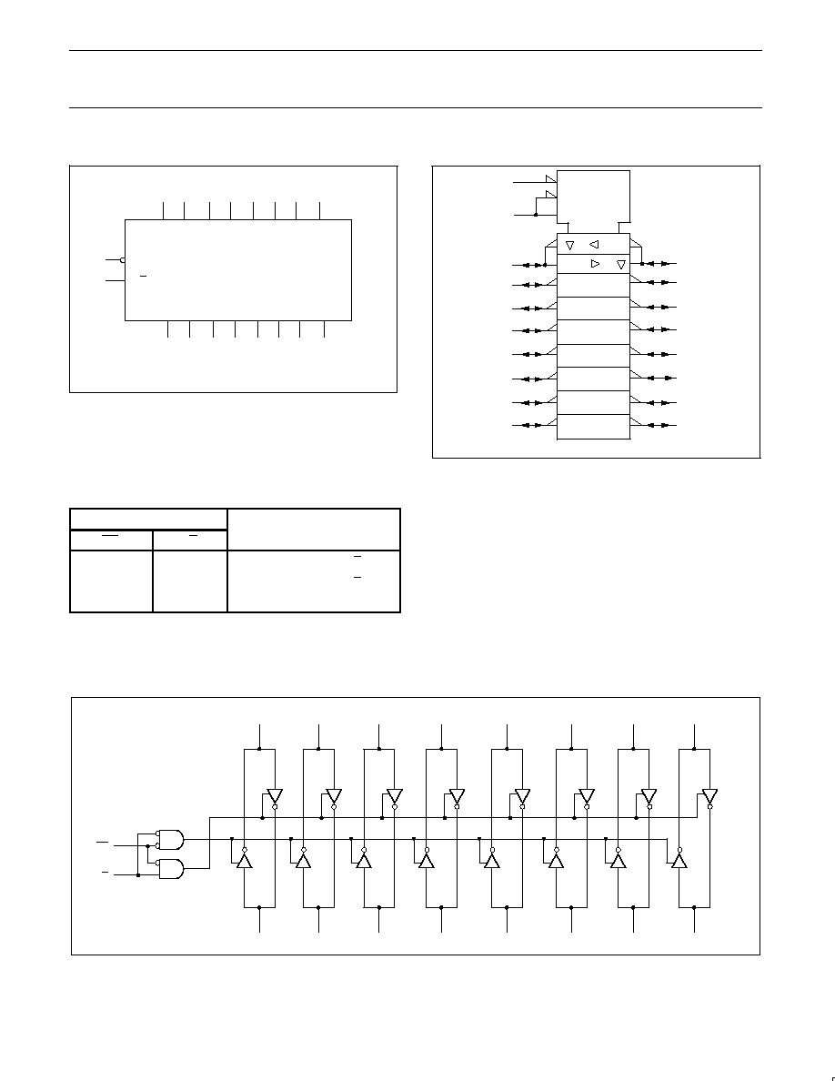
LOGIC SYMBOL
B0
B1
B2
B3
19
1
T/R
OE
SF01140
VCC = Pin 20
GND = Pin 10
B4
B5
B6
B7
8
9
A2
A3
4
5
6
A4
A5
A6
7
A7
2
3
A0
A1
18
17
16
15
14
13
12
11
LOGIC SYMBOL (IEEE/IEC)
SF01141
19
1
18
G3
3EN1(BA)
3EN2(AB)
1
17
16
15
14
13
12
11
3
4
5
6
7
8
9
2
2
FUNCTION TABLE
INPUTS
OUTPUTS
OE
T/R
OUTPUTS
L
L
Bus B data to Bus A
L
H
Bus A data to Bus B
H
X
Z
H = High voltage level
L
= Low voltage level
X = Don't care
Z = High impedance "off" state
LOGIC DIAGRAM
VCC =
Pin 20
GND =
Pin 10
SF01142
OE
T/R
19
1
2
3
4
18
17
16
15
14
13
12
B0
B1
B4
B5
B6
B7
A0
A1
A4
A5
A6
A7
B2
B3
A3
A2
5
6
7
8
11
9

Philips Semiconductors
Product specification
74F640
Octal bus transceiver, inverting (3-State)
1989 Nov 27
4
ABSOLUTE MAXIMUM RATINGS
(Operation beyond the limits set forth in this table may impair the useful life of the device.
Unless otherwise noted these limits are over the operating free-air temperature range.)
SYMBOL
PARAMETER
RATING
UNIT
V
CC
Supply voltage
≠0.5 to +7.0
V
V
IN
Input voltage
≠0.5 to +7.0
V
I
IN
Input current
≠30 to +5
mA
V
OUT
Voltage applied to output in High output state
≠0.5 to +V
CC
V
I
O
Current applied to output in Low output state
A0≠A7
48
mA
I
OUT
Current applied to output in Low output state
B0≠B7
128
mA
T
amb
Operating free-air temperature range
0 to +70
∞
C
T
stg
Storage temperature range
≠65 to +150
∞
C
RECOMMENDED OPERATING CONDITIONS
SYMBOL
PARAMETER
LIMITS
UNIT
SYMBOL
PARAMETER
MIN
NOM
MAX
UNIT
V
CC
Supply voltage
4.5
5.0
5.5
V
V
IH
High-level input voltage
2.0
V
V
IL
Low-level input voltage
0.8
V
I
IK
Input clamp current
≠18
mA
I
O
High level output current
A0≠A7
≠3
mA
I
OH
High-level output current
B0≠B7
≠15
mA
I
O
Low level output current
A0≠A7
24
mA
I
OL
Low-level output current
B0≠B7
64
mA
T
amb
Operating free-air temperature range
0
70
∞
C

Philips Semiconductors
Product specification
74F640
Octal bus transceiver, inverting (3-State)
1989 Nov 27
5
DC ELECTRICAL CHARACTERISTICS
(Over recommended operating free-air temperature range unless otherwise noted.)
NO TAG
LIMITS
SYMBOL
PARAMETER
TEST CONDITIONS
NO TAG
MIN
TYP
NO TAG
MAX
UNIT
A0≠A7
I
O
= 3mA
±
10%V
CC
2.4
V
V
O
High level output voltage
B0≠B7
V
CC
= MIN,
V
IL
= MAX
I
OH
= ≠3mA
±
5%V
CC
2.7
3.3
V
V
OH
High-level output voltage
B0 B7
V
IL
= MAX,
V
IH
= MIN
I
O
= 15mA
±
10%V
CC
2.0
V
B0≠B7
I
OH
= ≠15mA
±
5%V
CC
2.0
V
A0 A7
I
O
= 24mA
±
10%V
CC
0.35
0.50
V
V
O
Low level output voltage
A0≠A7
V
CC
= MIN,
V
IL
= MAX
I
OL
= 24mA
±
5%V
CC
0.35
0.50
V
V
OL
Low-level output voltage
B0 B7
V
IL
= MAX,
V
IH
= MIN,
I
O
= MAX
±
10%V
CC
0.55
V
B0≠B7
I
OL
= MAX
±
5%V
CC
0.42
0.55
V
V
IK
Input clamp voltage
V
CC
= MIN, I
I
= I
IK
≠0.73
≠1.2
V
I
I
Input current at maximum
OE,
T/R
V
CC
= 0.0V, V
I
= 7.0V
100
µ
A
I
I
input voltage
A0≠A7,
B0≠B7
V
CC
= 5.5V, V
I
= 5.5V
1.0
mA
I
IH
High-level input current
OE,
T/R
V
CC
= MAX, V
I
= 2.7V
40
µ
A
I
IL
Low-level input current
T/R
only
V
CC
= MAX, V
I
= 0.5V
≠40
µ
A
I
OZH
+I
IH
Off-state output current,
High level of voltage applied
V
CC
= MAX, V
I
= 2.7V
70
µ
A
I
OZL
+I
IL
Off-state output current,
Low level of voltage applied
V
CC
= MAX, V
I
= 0.5V
≠70
µ
A
I
OS
Short-circuit output cur-
NO TAG
A0≠A7
V
CC
= MAX
≠60
≠150
mA
I
OS
rent
NO TAG
B0≠B7
V
CC
= MAX
≠100
≠225
µ
A
I
CCH
T/R = An = 4.5V,
OE = GND
66
85
mA
I
CC
Supply current (total)
I
CCL
V
CC
= MAX
T/R = Bn = OE = GND
91
120
mA
I
CCZ
T/R = Bn = GND,
OE = 4.5V
78
102
mA
NOTES:
1. For conditions shown as MIN or MAX, use the appropriate value specified under recommended operating conditions for the applicable type.
2. All typical values are at V
CC
= 5V, T
amb
= 25
∞
C.
3. Not more than one output should be shorted at a time. For testing I
OS
, the use of high-speed test apparatus and/or sample-and-hold
techniques are preferable in order to minimize internal heating and more accurately reflect operational values. Otherwise, prolonged shorting
of a High output may raise the chip temperature well above normal and thereby cause invalid readings in other parameter tests. In any
sequence of parameter tests, I
OS
tests should be performed last.