 | –≠–ª–µ–∫—Ç—Ä–æ–Ω–Ω—ã–π –∫–æ–º–ø–æ–Ω–µ–Ω—Ç: N74F670N | –°–∫–∞—á–∞—Ç—å:  PDF PDF  ZIP ZIP |
Philips
Semiconductors
74F670
4 x 4 register file (3-State)
Product specification
IC15 Data Handbook
1990 Jul 12
INTEGRATED CIRCUITS
Philips Semiconductors
Product specification
74F670
4 x 4 register file (3-State)
2
1990 Jul 12
853-0014 99965
FEATURES
∑
Simultaneous and Independent Read and Write operations
∑
Expandable to almost any word size and bit length
∑
3-State outputs
DESCRIPTION
The 74F670 is a 16-bit 3-State Register File organized as 4 words of
4 bits each. Separate Read and Write Address and Enable inputs
are available, permitting simultaneous writing into one word location
and reading from another location. The 4-bit word to be stored is
presented to four data inputs.
The Write address inputs (WA and WB) determine the location of the
stored word. The Write Address inputs should only be changed
when the Write Enable input (WE) is High for conventional
operation. When the WE is Low, the data is entered into the
addressed location.
The addressed location remains transparent to the data while the
WE is Low. Data supplied at the inputs will be read out in true
(non-inverting) form from the 3-State outputs. Data and address
inputs are inhibited when the WE is High. Direct acquisition of data
stored in any of the four registers is made possible by individual
Read Address inputs (RA, RB). The addressed word appears at the
four outputs when the Read Enable (RE) is Low. Data outputs are in
the high impedance "off" state when the RE is High. This permits
outputs to be tied together to increase the word capacity to very
large numbers.
Up to 128 devices can be stacked to increase the word size to 512
locations by tying the 3-State outputs together. Since the limiting
factor for expansion is the output High current, further stacking is
possible by tying pullup reisistors to the outputs to increase the I
OH
current available. Design of the Read Enable signals for the stacked
devices must ensure that there is no overlap in the Low levels which
cause more than one output to be active at the same time. Parallel
expansion to generate n-bit words is accomplished by driving the
Enable and address inputs of each device in parallel.
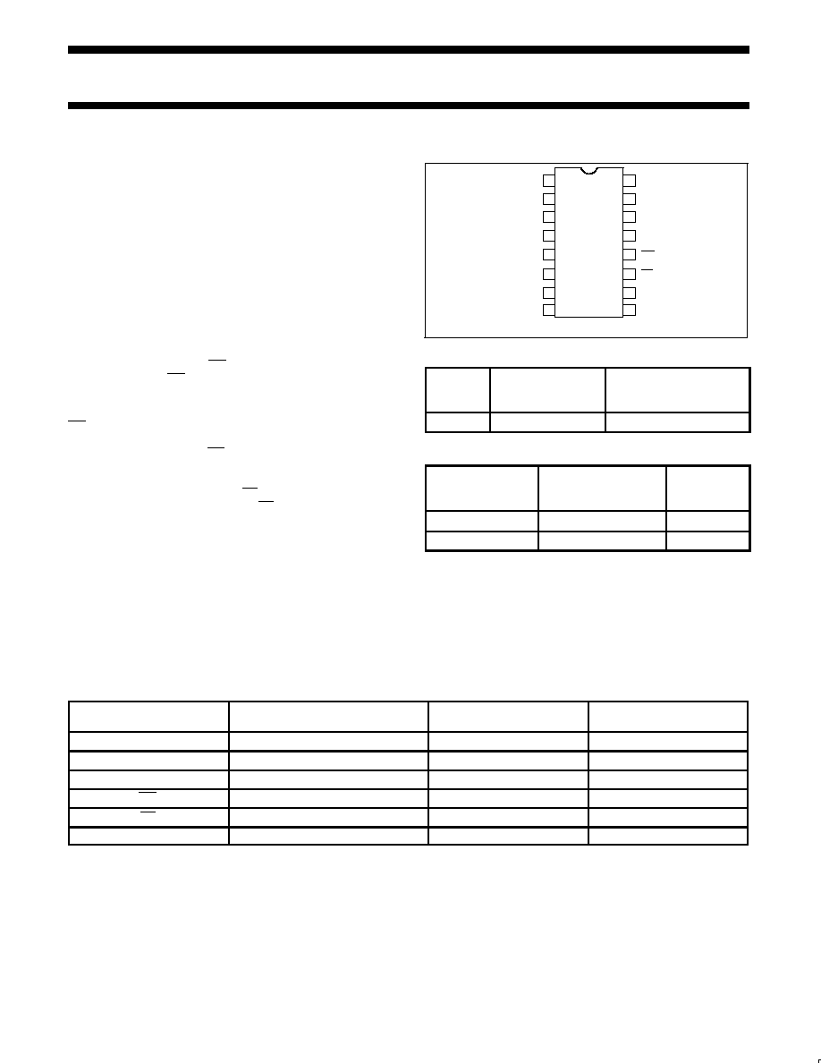
PIN CONFIGURATION
7
14
13
12
11
10
9
6
5
4
3
2
1
V
CC
D0
WE
RE
Q1
RA
D2
Q3
D1
GND
D3
RB
SF01178
Q0
WB
Q2
WA
8
16
15
TYPE
TYPICAL
PROPAGATION
DELAY
TYPICAL
SUPPLY CURRENT
(TOTAL)
74F670
6.5ns
50mA
ORDERING INFORMATION
DESCRIPTION
COMMERCIAL RANGE
V
CC
= 5V
±
10%,
T
amb
= 0
∞
C to +70
∞
C
PKG DWG #
16-pin plastic DIP
N74F670N
SOT38-4
16-pin plastic SOL
N74F670D
SOT162-1
INPUT AND OUTPUT LOADING AND FAN-OUT TABLE
PINS
DESCRIPTION
74F(U.L.)
HIGH/LOW
LOAD VALUE
HIGH/LOW
D0 - D3
Data inputs
1.0/1.0
20
µ
A/0.6mA
WA, WB
Write address inputs
1.0/1.0
20
µ
A/0.6mA
RA, RB
Read address inputs
1.0/1.0
20
µ
A/0.6mA
WE
Write Enable inputs
1.0/1.0
20mA/0.6mA
RE
Read Enable inputs
1.0/1.0
20mA/0.6mA
Q0≠Q3
Data output
150/40
3.0mA/24mA
NOTE:
One (1.0) FAST Unit Load is defined as: 20
µ
A in the High state and 0.6mA in the Low state.
Philips Semiconductors
Product specification
74F670
4 x 4 register file (3-State)
1990 Jul 12
3
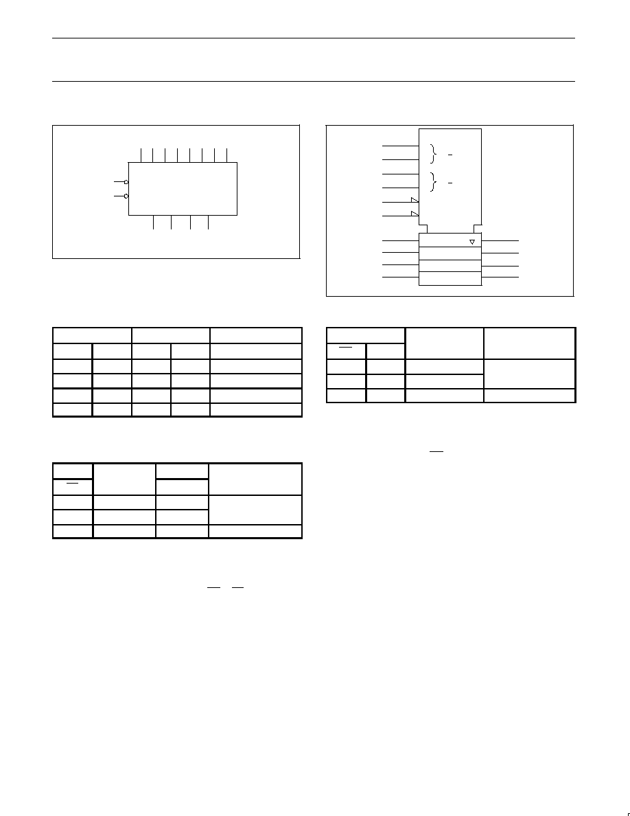
LOGIC SYMBOL
14 13
5
4
15
1
2
3
10
9
Q1
Q0
WA WB RA RB D0 D1 D2 D3
SF01179
7
6
Q3
Q2
12
WE
V
CC
=Pin 16
GND=Pin 8
RE
11
LOGIC SYMBOL (IEEE/IEC)
SF01180
RAM 4X4
14
13
12
11
15
1
10
9
7
6
0
1
1A
0
3
5
4
0
1
2A
0
3
C4 [WRITE]
EN [READ]
2
3
1A, 4D
2A
WORD SELECT FUNCTION TABLE
WRITE MODE
READ MODE
OPERATING MODE
WB
WA
RB
RA
Word Selected
L
L
L
L
Word 0
L
H
L
H
Word 1
H
L
H
L
Word 2
H
H
H
H
Word 3
H = High voltage level
L = Low voltage level
READ MODE FUNCTION TABLE
INPUT
INTERNAL
OUTPUT
OPERATING MODE
RE
LATCHES*
Qn
OPERATING MODE
L
L
L
Read
L
H
H
Read
H
X
Z
Disabled
H = High voltage level
L = Low voltage level
X = Don't care
Z = High impedance "off" state
*
= The selection of "internal latches" by Read Address
(RA and RB) are not constrained by WE or RE operation.
WRITE MODE FUNCTION TABLE
INPUTS
INTERNAL
OPERATING MODE
WE
Dn
LATCHES*
OPERATING MODE
L
L
L
Write data
L
H
H
Write data
H
X
NC
Data latched
H = High voltage level
L = Low voltage level
NC= No change
X = Don't care
*
= The write address (WA and WB) to the "internal latches"
must be stabled while WE is Low for conventional operation.
Philips Semiconductors
Product specification
74F670
4 x 4 register file (3-State)
1990 Jul 12
4
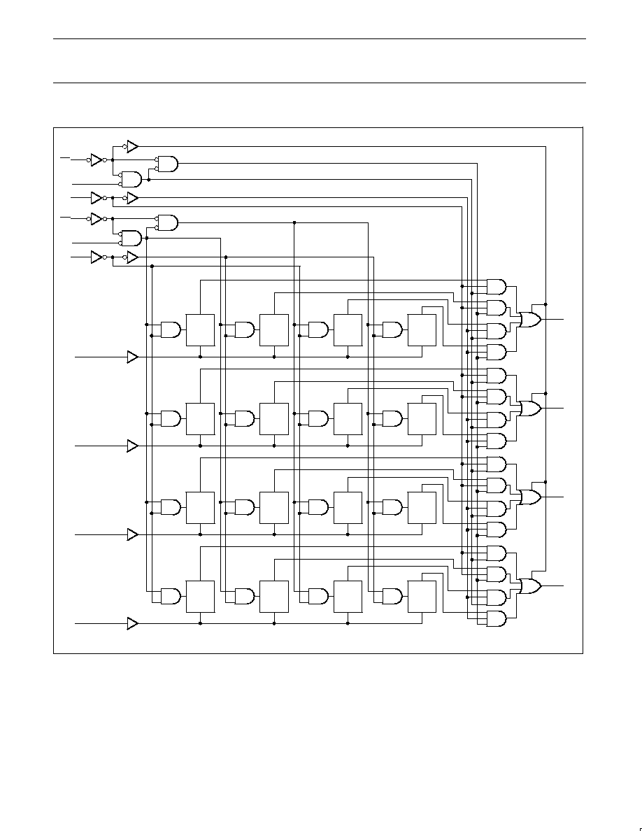
LOGIC DIAGRAM
6
Q3
V
CC
=Pin 16
GND=Pin 8
SF01181
E
Q
D
E
Q
D
E
Q
D
E
Q
D
7
Q2
E
Q
D
E
Q
D
E
Q
D
E
Q
D
9
Q1
E
Q
D
E
Q
D
E
Q
D
E
Q
D
10
Q0
E
Q
D
E
Q
D
E
Q
D
E
Q
D
11
5
4
12
13
14
3
2
1
15
RE
RA
RB
WE
WB
WA
D3
D2
D1
D0
Philips Semiconductors
Product specification
74F670
4 x 4 register file (3-State)
1990 Jul 12
5
ABSOLUTE MAXIMUM RATINGS
(Operation beyond the limits set forth in this table may impair the useful life of the device.
Unless otherwise noted these limits are over the operating free-air temperature range.)
SYMBOL
PARAMETER
RATING
UNIT
V
CC
Supply voltage
≠0.5 to +7.0
V
V
IN
Input voltage
≠0.5 to +7.0
V
I
IN
Input current
≠30 to +5
mA
V
OUT
Voltage applied to output in High output state
≠0.5 to V
CC
V
I
OUT
Current applied to output in Low output state
48
mA
T
amb
Operating free-air temperature range
0 to +70
∞
C
T
stg
Storage temperature
≠65 to +150
∞
C
RECOMMENDED OPERATING CONDITIONS
SYMBOL
PARAMETER
LIMITS
UNIT
SYMBOL
PARAMETER
MIN
NOM
MAX
UNIT
V
CC
Supply voltage
4.5
5.0
5.5
V
V
IH
High-level input voltage
2.0
V
V
IL
Low-level input voltage
0.8
V
I
IK
Input clamp current
≠18
mA
I
OH
High-level output current
≠3
mA
I
OL
Low-level output current
24
mA
T
amb
Operating free-air temperature range
0
70
∞
C
DC ELECTRICAL CHARACTERISTICS
(Over recommended operating free-air temperature range unless otherwise noted.)
NO TAG
LIMITS
SYMBOL
PARAMETER
TEST CONDITIONS
NO TAG
MIN
TYP
NO TAG
MAX
UNIT
V
O
High level output voltage
V
CC
= MIN, V
IL
= MAX
±
10%V
CC
2.4
V
V
OH
High-level output voltage
V
IH
= MIN, I
OH
= MAX
±
5%V
CC
2.7
3.4
V
V
O
Low level output voltage
V
CC
= MIN, V
IL
= MAX
±
10%V
CC
0.35
0.50
V
V
OL
Low-level output voltage
V
IH
= MIN, I
OL
= MAX
±
5%V
CC
0.35
0.50
V
V
IK
Input clamp voltage
V
CC
= MIN, I
I
= I
IK
≠0.73
≠1.2
V
I
I
Input current at maximum input voltage
V
CC
= MAX, V
I
= 7.0V
100
µ
A
I
IH
High-level input current
V
CC
= MAX, V
I
= 2.7V
20
µ
A
I
IL
Low-level input current
V
CC
= MAX, V
I
= 0.5V
≠0.6
mA
I
OZH
Off state output current,
High-level voltage applied
V
CC
= MAX, V
O
= 2.7V
50
µ
A
I
OZL
Off state output current,
Low-level voltage applied
V
CC
= MAX, V
O
= 0.5V
≠50
µ
A
I
OS
Short-circuit output current
NO TAG
V
CC
= MAX
≠60
≠150
mA
I
CCH
50
70
mA
I
CC
Supply current (total)
I
CCL
V
CC
= MAX
50
70
mA
I
CCZ
55
80
mA
NOTES:
1. For conditions shown as MIN or MAX, use the appropriate value specified under recommended operating conditions for the applicable type.
2. All typical values are at V
CC
= 5V, T
amb
= 25
∞
C.
3. Not more than one output should be shorted at a time. For testing I
OS
, the use of high-speed test apparatus and/or sample-and-hold
techniques are preferable in order to minimize internal heating and more accurately reflect operational values. Otherwise, prolonged shorting