 | –≠–ª–µ–∫—Ç—Ä–æ–Ω–Ω—ã–π –∫–æ–º–ø–æ–Ω–µ–Ω—Ç: N74F674N | –°–∫–∞—á–∞—Ç—å:  PDF PDF  ZIP ZIP |
Document Outline
- FEATURES
- DESCRIPTION
- PIN CONFIGURATION
- ORDERING INFORMATION
- INPUT AND OUTPUT LOADING AND FAN-OUT TABLE
- LOGIC SYMBOL
- LOGIC SYMBOL (IEEE/IEC)
- FUNCTION TABLE
- LOGIC DIAGRAM
- ABSOLUTE MAXIMUM RATINGS
- RECOMMENDED OPERATING CONDITIONS
- DC ELECTRICAL CHARACTERISTICS
- AC ELECTRICAL CHARACTERISTICS
- AC SETUP REQUIREMENTS
- AC WAVEFORMS
- TEST CIRCUIT AND WAVEFORM

Philips Semiconductors
Product specification
74F674
16-bit serial/parallel-in, serial-out shift register (3-State)
1
1989 Feb 05
853≠1248 92263
FEATURES
∑
16-bit serial I/O shift register
∑
16-bit parallel-in/serial-out converter
∑
Recirculating serial shifting
∑
Common serial data I/O pin (3-State)
DESCRIPTION
The 74F674 is a 16-bit shift register with serial and parallel load
capability and serial output. A single pin serves alternately as an
input for serial entry or as a 3-State serial output. In the serial out
mode the data recirculates in the register. Chip Select, Read/Write
and Mode inputs provide control flexibility. The 74F674 operates in
one of four modes, as indicated in the Function table.
Hold: A High signal on the Chip Select (CS) input prevents clocking
and forces the Serial Input/Output (SI/O) 3-State buffer into the high
impedance state.
Serial load: Data present on the SI/O pin shifts into the register on
the falling edge of CP. Data enters the Q0 position and shifts toward
Q15 on successive clocks.
Serial output: The SI/O 3-State buffer is active and the register
contents are shifted out from Q15 and simultaneously shifted back
into Q0.
Parallel load: Data present on D0≠D15 is entered into the register
on the falling edge of CP. The SI/O 3-State buffer is active and
represents the Q15 output. To prevent false clocking, CP must be
Low during a Low-to-High transition of CS.
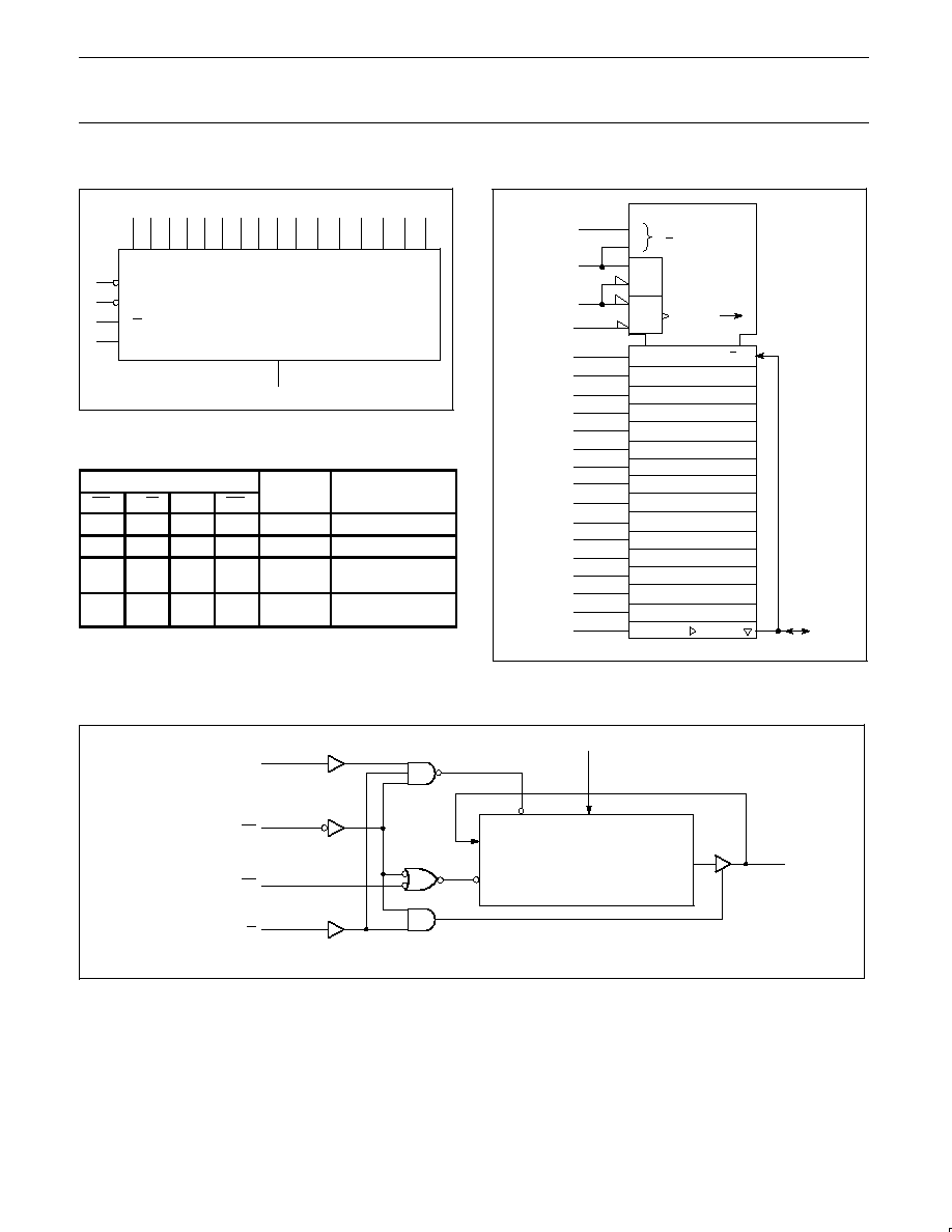
PIN CONFIGURATION
24
1
V
CC
CS
23
22
21
20
19
18
17
16
10
15
9
8
7
6
5
4
3
2
D15
D14
D11
D10
D9
D8
CP
M
SI/O
D1
D2
D3
D13
D12
NC
R/W
SF01188
D0
D7
14
12
13
11
D6
D4
GND
D5
TYPE
TYPICAL f
MAX
TYPICAL SUPPLY
CURRENT
(TOTAL)
74F674
95MHz
55mA
ORDERING INFORMATION
DESCRIPTION
COMMERCIAL RANGE
V
CC
= 5V
±
10%, T
amb
= 0
∞
C to +70
∞
C
24-Pin Plastic Slim DIP
(300mil)
N74F674N
24-Pin Plastic SOL
N74F674D
INPUT AND OUTPUT LOADING AND FAN-OUT TABLE
PINS
DESCRIPTION
74F(U.L.)
HIGH/LOW
LOAD VALUE
HIGH/LOW
D0≠D15
Parallel data inputs
1.0/1.0
20
µ
A/0.6mA
CS
Chip Select input (active Low)
1.0/1.0
20
µ
A/0.6mA
CP
Clock Pulse input (active falling edge)
1.0/1.0
20
µ
A/0.6mA
M
Mode select input
1.0/1.0
20
µ
A/0.6mA
R/W
Read/Write input
1.0/1.0
20
µ
A/0.6mA
SI/O
Serial data input or
3.5/1.0
70mA/0.6mA
SI/O
Serial 3-state output
150/40
3.0mA/24mA
NOTE: One (1.0) FAST Unit Load is defined as: 20
µ
A in the High state and 0.6mA in the Low state.
Philips Semiconductors
Product specification
74F674
16-bit serial/parallel-in, serial-out shift register (3-State)
1989 Feb 05
2
LOGIC SYMBOL
8
9
10
V
CC
= Pin 24
GND = Pin 12
1
2
SF01189
CP
CS
D0 D1
D4 D5 D6 D7
D3
D2
11 13
14
7
16 17
18
D8 D9
D12 D13 D14 D15
D11
D10
19
20
21
22
15
23
3
5
M
R/W
SO
6
FUNCTION TABLE
CONTROL INPUTS
SI/O
OPERATING
CS
R/W
M
CP
SI/O
STATUS
OPERATING
MODE
H
X
X
X
High Z
Hold
L
L
X
Data in
Serial load
L
H
L
Data out
Serial output with
recirculation
L
H
H
Active
Parallel load;
no shifting
H = High voltage level
L = Low voltage level
X = Don't care
= High-to-Low transition of designed input
LOGIC SYMBOL (IEEE/IEC)
SF01190
SRG16
0
1
M
0
3
3, 4D
5
3
1
2
8
9
10
11
13
14
7
16
17
18
19
20
21
22
15
23
3, 4D
3, 4D
3, 4D
&
&
EN
C4(0/1/2)
6
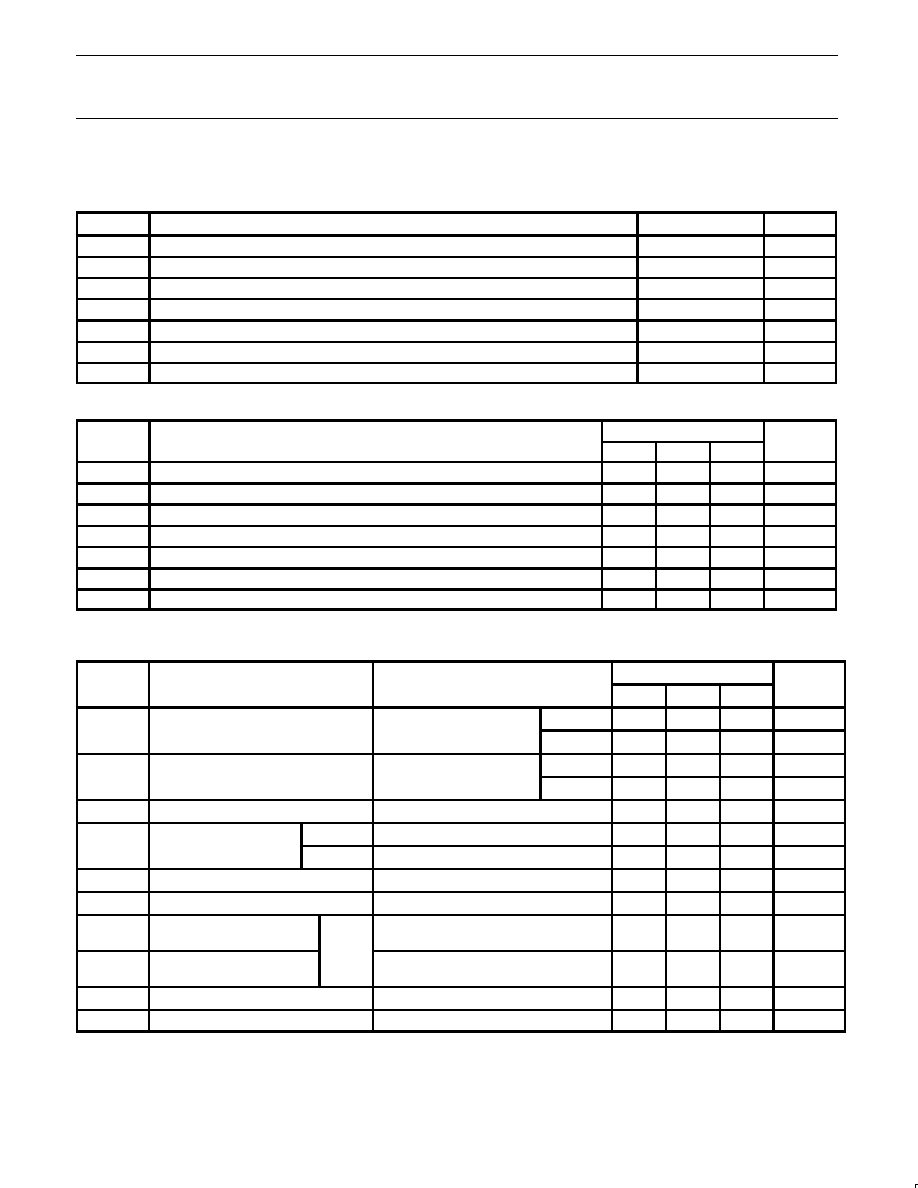
LOGIC DIAGRAM
VCC =
Pin 24
GND =
Pin 12
SF01191
PE
D0≠D15
Q15
CP
Q0
D0≠D15 (7≠11, 13≠23)
5
1
2
3
6
SI/O
M
CS
CP
R/W
Philips Semiconductors
Product specification
74F674
16-bit serial/parallel-in, serial-out shift register (3-State)
1989 Feb 05
3
ABSOLUTE MAXIMUM RATINGS
(Operation beyond the limits set forth in this table may impair the useful life of the device.
Unless otherwise noted these limits are over the operating free-air temperature range.)
SYMBOL
PARAMETER
RATING
UNIT
V
CC
Supply voltage
≠0.5 to +7.0
V
V
IN
Input voltage
≠0.5 to +7.0
V
I
IN
Input current
≠30 to +5.0
mA
V
OUT
Voltage applied to output in High output state
≠0.5 to +V
CC
V
I
OUT
Current applied to output in Low output state
48
mA
T
amb
Operating free-air temperature range
0 to +70
∞
C
T
stg
Storage temperature
≠65 to +150
∞
C
RECOMMENDED OPERATING CONDITIONS
SYMBOL
PARAMETER
LIMITS
UNIT
SYMBOL
PARAMETER
MIN
NOM
MAX
UNIT
V
CC
Supply voltage
4.5
5.0
5.5
V
V
IH
High-level input voltage
2.0
V
V
IL
Low-level input voltage
0.8
V
I
IK
Input clamp current
≠18
mA
I
OH
High-level output current
≠3
mA
I
OL
Low-level output current
24
mA
T
amb
Operating free-air temperature range
0
70
∞
C
DC ELECTRICAL CHARACTERISTICS
(Over recommended operating free-air temperature range unless otherwise noted.)
SYMBOL
PARAMETER
TEST CONDITIONS
1
LIMITS
UNIT
SYMBOL
PARAMETER
TEST CONDITIONS
1
MIN
TYP
2
MAX
UNIT
V
OH
High-level output voltage
V
CC
= MIN, V
IL
= MAX,
±
10%V
CC
2.4
V
V
OH
High-level output voltage
V
CC
MIN, V
IL
MAX,
V
IH
= MIN, I
OH
= MAX
±
5%V
CC
2.7
3.3
V
V
OL
Low-level output voltage
V
CC
= MIN, V
IL
= MAX,
±
10%V
CC
0.35
0.50
V
V
OL
Low-level output voltage
V
CC
MIN, V
IL
MAX,
V
IH
= MIN, I
OL
= MAX
±
5%V
CC
0.35
0.50
V
V
IK
Input clamp voltage
V
CC
= MIN, I
I
= I
IK
≠0.73
≠1.2
V
I
I
Input current at
SI/O only
V
CC
= MAX, V
I
= 5.5V
100
µ
A
I
I
Input current at
maximum input voltage
others
V
CC
= MAX, V
I
= 7.0V
100
µ
A
I
IH
High-level input current
V
CC
= MAX, V
I
= 2.7V
20
µ
A
I
IL
Low-level input current
V
CC
= MAX, V
I
= 0.5V
≠0.6
mA
I
OZH
+I
IH
Off-state output current
High-level voltage applied
SI/O
V
CC
= MAX, V
O
= 2.7V
70
µ
A
I
OZL
+I
IL
Off-state output current
Low-level voltage applied
SI/O
only
V
CC
= MAX, V
O
= 0.5V
≠600
µ
A
I
OS
Short-circuit output current
3
V
CC
= MAX
≠60
≠150
mA
I
CC
Supply current (total)
V
CC
= MAX
55
80
mA
NOTES:
1. For conditions shown as MIN or MAX, use the appropriate value under the recommended operating conditions for the applicable type.
2. All typical values are at V
CC
= 5V, T
amb
= 25
∞
C.
3. Not more than one output should be shorted at a time. For testing I
OS
, the use of high-speed test apparatus and/or sample-and-hold
techniques are preferable in order to minimize internal heating and more accurately reflect operational values. Otherwise, prolonged shorting
of a High output may raise the chip temperature well above normal and thereby cause invalid readings in other parameter tests. In any
sequence of parameter tests, I
OS
should be performed last.

Philips Semiconductors
Product specification
74F674
16-bit serial/parallel-in, serial-out shift register (3-State)
1989 Feb 05
4
AC ELECTRICAL CHARACTERISTICS
SYMBOL
PARAMETER
TEST
LIMITS
UNIT
SYMBOL
PARAMETER
TEST
T
amb
= +25
∞
C
T
amb
= 0
∞
C to +70
∞
C
UNIT
SYMBOL
PARAMETER
TEST
CONDITIONS
V
CC
= +5.0V
V
CC
= +5.0V
±
10%
UNIT
CONDITIONS
C
L
= 50pF, R
L
= 500
C
L
= 50pF, R
L
= 500
MIN
TYP
MAX
MIN
MAX
f
MAX
Maximum clock frequency
Waveform 1
80
95
70
MHz
t
PLH
t
PHL
Propagation delay
CP to SI/O
Waveform 1
7.0
6.0
9.5
8.5
12.5
11.5
6.5
5.5
14.0
12.5
ns
ns
t
PZH
t
PZL
Output Enable time
CS to SI/O
Waveform 3
Waveform 4
5.5
7.0
8.5
9.5
11.0
12.5
5.0
6.5
12.5
14.0
ns
ns
t
PHZ
t
PLZ
Output Disable time
CS to SI/O
Waveform 3
Waveform 4
3.0
4.5
6.0
7.5
8.5
10.0
3.0
4.5
10.0
11.5
ns
ns
t
PZH
t
PZL
Output Enable time
R/W to SI/O
Waveform 3
Waveform 4
6.0
7.5
8.5
10.0
11.5
13.0
5.5
7.0
13.0
14.0
ns
ns
t
PHZ
t
PLZ
Output Disable time
R/W to SI/O
Waveform 3
Waveform 4
5.0
5.5
7.5
8.0
10.5
11.0
4.5
5.0
12.0
13.5
ns
ns
AC SETUP REQUIREMENTS
SYMBOL
PARAMETER
TEST CONDITION
LIMITS
UNIT
SYMBOL
PARAMETER
TEST CONDITION
T
amb
= +25
∞
C
T
amb
= 0
∞
C to +70
∞
C
UNIT
SYMBOL
PARAMETER
TEST CONDITION
V
CC
= +5.0V
V
CC
= +5.0V
±
10%
UNIT
C
L
= 50pF, R
L
= 500
C
L
= 50pF, R
L
= 500
MIN
TYP
MAX
MIN
MAX
t
s
(H)
t
s
(L)
Setup time, High or Low
SI/O to CP
Waveform 2
2.0
2.0
2.5
2.5
ns
ns
t
h
(H)
t
h
(L)
Hold time, High or Low
SI/O to CP
Waveform 2
1.5
1.5
2.0
2.0
ns
ns
t
s
(H)
t
s
(L)
Setup time, High or Low
Dn to CP
Waveform 2
1.5
1.0
2.0
1.0
ns
ns
t
h
(H)
t
h
(L)
Hold time, High or Low
Dn to CP
Waveform 2
3.0
4.0
3.0
4.0
ns
ns
t
s
(H)
t
s
(L)
Setup time, High or Low
M to CP
Waveform 2
2.0
5.5
2.5
6.0
ns
ns
t
h
(H)
t
h
(L)
Hold time, High or Low
M to CP
Waveform 2
0.0
0.0
1.0
1.0
ns
ns
t
s
(L)
Setup time, Low
CS to CP
Waveform 2
8.0
9.0
ns
t
h
(H)
Hold time, High
CS to CP
Waveform 2
0.0
0.0
ns
t
w
(H)
t
w
(L)
CP Pulse width,
High or Low
Waveform 1
3.5
4.5
4.0
5.0
ns
ns

Philips Semiconductors
Product specification
74F674
16-bit serial/parallel-in, serial-out shift register (3-State)
1989 Feb 05
5
AC WAVEFORMS
For all waveforms, V
M
= 1.5V.
The shaded areas indicate when the input is permitted to change for predictable output performance.
tW(H)
CP
SI/O
VM
VM
VM
VM
VM
1/fMAX
tW(L)
tPHL
tPLH
SF01192
Waveform 1. Propagation Delay, Clock Input to Output,
Clock Pulse Width, and Maximum Clock Frequency
VM
VM
VM
VM
VM
VM
ts(H)
ts(L)
th(H)
th(L)
CP
Dn, CS,
M, R/W,
SI/O
SF01193
Waveform 2. Setup and Hold Times
V
M
V
M
V
M
t
PHZ
t
PZH
CS, R/W
SI/O
V
OH
-0.3V
0V
SF01194
Waveform 3. 3-State Output Enable Time to High Level
and Output Disable Time from High Level
V
M
V
M
V
M
t
PLZ
t
PZL
CS, R/W
SI/O
V
OL
+0.3V
SF01195
Waveform 4. 3-State Output Enable Time to Low Level
and Output Disable Time from Low Level
TEST CIRCUIT AND WAVEFORM
tw
90%
VM
10%
90%
VM
10%
90%
VM
10%
90%
VM
10%
NEGATIVE
PULSE
POSITIVE
PULSE
tw
AMP (V)
0V
0V
tTHL (tf
)
INPUT PULSE REQUIREMENTS
rep. rate
t
w
t
TLH
t
THL
1MHz
500ns
2.5ns
2.5ns
Input Pulse Definition
VCC
family
74F
D.U.T.
PULSE
GENERATOR
RL
CL
RT
VIN
VOUT
Test Circuit for 3-State Outputs
DEFINITIONS:
R
L
= Load resistor;
see AC electrical characteristics for value.
C
L
= Load capacitance includes jig and probe capacitance;
see AC electrical characteristics for value.
R
T
= Termination resistance should be equal to Z
OUT
of
pulse generators.
tTHL (tf
)
tTLH (tr
)
tTLH (tr
)
AMP (V)
amplitude
3.0V
1.5V
V
M
RL
7.0V
SF00777
TEST
SWITCH
t
PLZ
closed
t
PZL
closed
All other
open
SWITCH POSITION