Philips Semiconductors
Product specification
74F779
8-bit bidirectional binary counter (3-State)
2
1989 Sep 20
853≠0385 97676
FEATURES
∑
Multiplexed 3-State I/O ports for bus oriented applications
∑
Built-in look-ahead carry capability
∑
Center power pins to reduce effects of package inductance
∑
Count frequency 145MHz typical
∑
Supply current 90mA typical
∑
See 74F269 for 24-pin separate I/O port version
∑
See 74F579 for 20-pin version
∑
See 74F1779 for extended function version of the 74F799
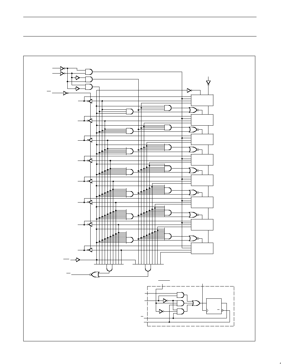
DESCRIPTION
The 74F779 is a fully synchronous 8-stage Up/Down Counter with
multiplexed 3-State I/O ports for bus-oriented applications. All
control functions (hold, count up, count down, synchronous load) are
controlled by two mode pine (S0, S1). The device also features
carry look-ahead for easy cascading. All state changes are initiated
by the rising edge of the clock. When CET is High the data outputs
are held in their current state and TC is held High. The TC output is
not recommended for use as a clock or asynchronous reset due to
the possibility of decoding spikes.
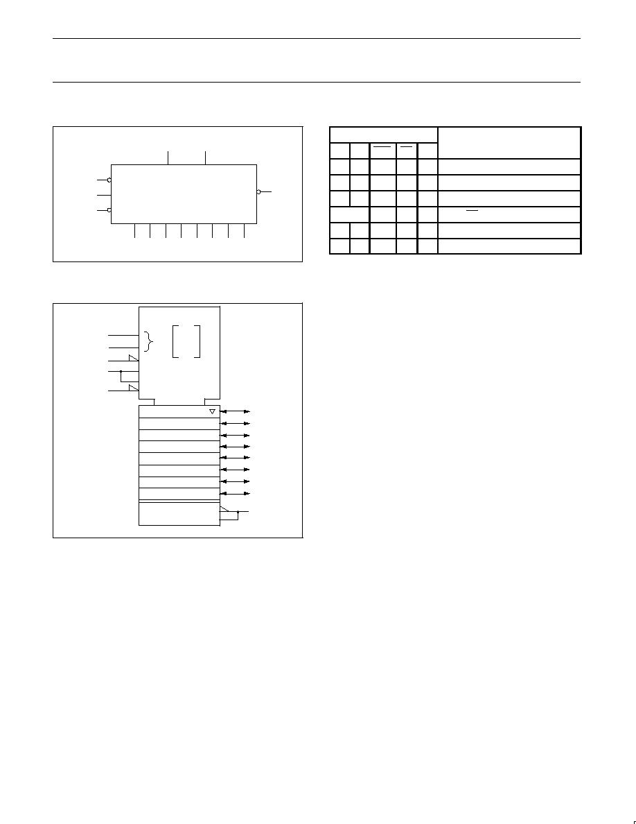
PIN CONFIGURATION
16
15
14
13
12
11
10
9
8
7
6
5
4
3
2
1
I/O1
I/O0
CP
CET
V
CC
TC
S0
S1
OE
I/O2
I/O3
GND
I/O4
I/O5
I/O7
I/O6
SF01259
TYPE
TYPICAL f
MAX
TYPICAL
SUPPLY CURRENT
(TOTAL)
74F779
145MHz
90mA
ORDERING INFORMATION
DESCRIPTION
COMMERCIAL RANGE
V
CC
= 5V
±
10%,
T
amb
= 0
∞
C to +70
∞
C
PKG DWG #
16-Pin Plastic DIP
N74F779N
SOT38-4
16-Pin Plastic SOL
N74F779D
SOT 162-1
INPUT AND OUTPUT LOADING AND FAN-OUT TABLE
PINS
DESCRIPTION
74F(U.L.)
HIGH/LOW
LOAD VALUE
HIGH/LOW
I/On
Data inputs
3.5/1.0
70
µ
A/0.6mA
I/On
Data outputs
150/40
3.0mA/24mA
S0, S1
Select inputs
1.0/1.0
20
µ
A/0.6mA
OE
Output Enable input (active Low)
1.0/1.0
20
µ
A/0.6mA
CET
Count Enable Trickle input (active Low)
1.0/1.0
20
µ
A/0.6mA
CP
Clock input (active rising edge)
1.0/1.0
20
µ
A/0.6mA
TC
Terminal Count output (active Low)
50/33
1.0mA/20mA
NOTE:
One (1.0) FAST Unit Load is defined as: 20
µ
A in the High state and 0.6mA in the Low state.
Philips Semiconductors
Product specification
74F779
8-bit bidirectional binary counter (3-State)
1989 Sep 20
3
LOGIC SYMBOL
I/O0 I/O1 I/O2 I/O3 I/O4 I/O5 I/O6 I/O7
15
16
1
2
3
5
6
7
8
12
TC
9
14
OE
CET
CP
V
CC
=Pin 13
GND=Pin 4
SF01260
S0
S1
11
10
LOGIC SYMBOL (IEEE/IEC)
SF01261
EN4
11
15
14
9
[1]
[2]
[4]
[8]
[16]
[32]
[64]
[128]
4, 5, 8 CT=256
4, 5, 8 CT=0
12
16
1
2
3
5
6
7
8
CTR DIV 256
10
0
1
M
0
3
--
EN6
1≠
2 +/C5
LOAD
DOWN
UP
HOLD
6
FUNCTION TABLE
INPUTS
OPERATING MODE
S1
S0
CET
OE
CP
X
X
X
H
X
I/O0 to I/O7 in High impedance
X
X
X
L
X
Flip-flop outputs appear on I/O lines
L
L
X
H
Parallel load all flip-flops
(not LL)
H
X
Hold (TC held High)
H
L
L
X
Count up
L
H
L
X
Count down
H = High voltage level
L = Low voltage level
X = Don't care
= Low-to-High clock transition
(not LL) = S0 and S1 should never be Low voltage level at the
same time in the hold mode only.

Philips Semiconductors
Product specification
74F779
8-bit bidirectional binary counter (3-State)
1989 Sep 20
5
ABSOLUTE MAXIMUM RATINGS
(Operation beyond the limits set forth in this table may impair the useful life of the device.
Unless otherwise noted these limits are over the operating free-air temperature range.)
SYMBOL
PARAMETER
RATING
UNIT
V
CC
Supply voltage
≠0.5 to +7.0
V
V
IN
Input voltage
≠0.5 to +7.0
V
I
IN
Input current
≠30 to +5
mA
V
OUT
Voltage applied to output in High output state
≠0.5 to V
CC
V
I
O
Current applied to output in Low output state
TC
40
mA
I
OUT
Current applied to output in Low output state
I/On
48
mA
T
amb
Operating free-air temperature range
0 to +70
∞
C
T
stg
Storage temperature
≠65 to +150
∞
C
RECOMMENDED OPERATING CONDITIONS
SYMBOL
PARAMETER
LIMITS
UNIT
SYMBOL
PARAMETER
MIN
NOM
MAX
UNIT
V
CC
Supply voltage
4.5
5.0
5.5
V
V
IH
High-level input voltage
2.0
V
V
IL
Low-level input voltage
0.8
V
I
IK
Input clamp current
≠18
mA
I
O
High level output current
TC
≠1
mA
I
OH
High-level output current
I/On
≠3
mA
I
O
Low level output current
TC
20
mA
I
OL
Low-level output current
I/On
24
mA
T
amb
Operating free-air temperature range
0
70
∞
C