 | –≠–ª–µ–∫—Ç—Ä–æ–Ω–Ω—ã–π –∫–æ–º–ø–æ–Ω–µ–Ω—Ç: N74F786N | –°–∫–∞—á–∞—Ç—å:  PDF PDF  ZIP ZIP |

Philips
Semiconductors
74F786
4-bit asynchronous bus arbiter
Product specification
IC15 Data Handbook
1991 Feb 14
INTEGRATED CIRCUITS
Philips Semiconductors
Product specification
74F786
4-bit asynchronous bus arbiter
2
February 14, 1991
853≠1269 01717
FEATURES
∑
Arbitrates between 4 asynchronous inputs
∑
Separate grant output for each input
∑
Common output enable
∑
On board 4 input AND gate
∑
Metastable≠free outputs
∑
Industrial temperature range available (≠40
∞
C to +85
∞
C)
DESCRIPTION
The 74F786 is an asynchronous 4≠bit arbiter designed for high
speed real≠time applications. The priority of arbitration is determined
on a first≠come first≠served basis. Separate bus grant (BGn)
outputs are available to indicate which one of the request inputs is
served by the arbitration logic. All BGn outputs are enabled by a
common enable (EN) pin. In order to generate a bus request signal
a separate 4 input AND gate is provided which may also be used as
an independent AND gate. Unused bus request (BR) inputs may be
disabled by tying them high.
The 74F786 is designed so that contention between two or more
request signals will not glitch or display a metastable condition. In
this situation an increase in the BRn to BGn t
PHL
may be observed.
A typical 74F786 has an h = 6.6ns, t = 0.41ns and To = 5
µ
sec.
Where:
h = Typical propagation delay through the device and t and To are
device parameters derived from test results and can most nearly be
defined as:
t = A function of the rate at which a latch in a metastable state
resolves that condition.
To = A function of the measurement of the propensity of a latch to
enter a metastable state. To is also a very strong function of the
normal propagation delay of the device.
For further information, please refer to the 74F786 application notes.
TYPE
TYPICAL
PROPAGATION DELAY
TYPICAL
SUPPLY CURRENT
(TOTAL)
74F786
6.6ns
55mA
ORDERING INFORMATION
ORDER CODE
COMMERCIAL RANGE
INDUSTRIAL RANGE
DESCRIPTION
V
CC
= 5V
±
10%,
V
CC
= 5V
±
10%,
PKG DWG #
T
amb
= 0
∞
C to +70
∞
C
T
amb
= ≠40
∞
C to +85
∞
C
16≠pin plastic DIP
N74F786N
I74F786N
SOT 38-4
16≠pin plastic SO
N74F786D
I74F786D
SOT109-1
INPUT AND OUTPUT LOADING AND FAN OUT TABLE
PINS
DESCRIPTION
74F (U.L.) HIGH/
LOW
LOAD VALUE HIGH/
LOW
BR0 ≠ BR3
Bus request inputs (active low)
1.0/3.0
20
µ
A/1.8mA
A, B, C, D
AND gate inputs
1.0/1.0
20
µ
A/0.6mA
EN
Common bus grant output enable input (active low)
1.0/1.0
20
µ
A/0.6mA
YOUT
AND gate output
150/40
3.0mA/24mA
BG0 ≠ BG3
Bus grant outputs (active low)
150/40
3.0mA/24mA
NOTE:
One (1.0) FAST unit load is defined as: 20
µ
A in the high state and 0.6mA in the low state.
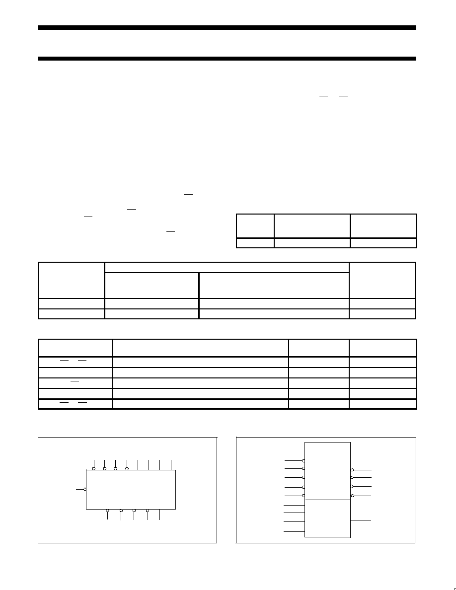
LOGIC SYMBOL
BR0 BR1 BR2 BR3
A
B
C
D
VCC = Pin 16
GND = Pin 8
BG0
BG1
BG2
BG3 YOUT
EN
6
13
12
11
10
14
4
5
6
7
15
1
2
3
SF00442
IEC/IEEE SYMBOL
BUS ARBITER
74F786
14
9
4
5
6
7
EN
BR0
BR1
BR2
BR3
15
1
2
3
&
13
12
11
10
BG0
BG1
BG2
BG3
SF00443

Philips Semiconductors
Product specification
74F786
4-bit asynchronous bus arbiter
February 14, 1991
3
FUNCTIONAL DESCRIPTION
The BRn inputs have no inherent priority. The arbiter assigns priority
to the incoming requests as they are received, therefore, the first BR
asserted will have the highest priority. When a bus request is
received its corresponding bus grant becomes active, provided that
EN is low. If additional bus requests are made during this time they
are queued. When the first request is removed, the arbiter services
the bus request with the next highest priority. Removing a request
while a previous request is being serviced can cause a grant to be
changed when arbitrating between three or four requests. For that
reason, the user should not remove ungranted requests when
arbitrating between three or four requests. This does not apply to
arbitration between two requests.
If two or more BRn inputs are asserted at precisely the same time,
one of them will be selected at random, and all BGn outputs will be
held in the high state until the selection is made. This guarantees
that an erroneous BGn will not be generated even though a
metastable condition may occur internal to the device. When the EN
is in the high state the BGn outputs are forced high.
PIN CONFIGURATION
16
15
14
13
12
11
10
7
6
5
4
3
2
1
9
8
VCC
B
C
D
BR0
BR1
BR2
BR3
GND
A
YOUT
BG0
BG1
BG2
BG3
EN
SF00441
PIN DESCRIPTION
SYMBOL
PINS
TYPE
NAME
FUNCTION
BR0 ≠ BR3
4, 5, 6, 7
Input
Bus request inputs (active low)
The logic of this device arbitrates between these four inputs.
Unused inputs should be tied high.
A, B, C, D
15, 1, 2, 3
Input
Inputs of the 4≠input AND gate
EN
9
Input
Enable input
When low it enables the BG0 ≠ BG3 outputs.
BG0 ≠ BG3
13, 12, 11, 10
Output
Bus grant outputs (active low)
These outputs indicate the selected bus request. BG0 corre-
sponds to BR0, BG1 to BR1, etc.
YOUT
14
Output
Output of the 4≠input AND gate
GND
8
Ground
ground (0V)
V
CC
16
Power
Positive supply voltages
Philips Semiconductors
Product specification
74F786
4-bit asynchronous bus arbiter
February 14, 1991
4
ARBITER FUNCTION TABLE
INPUTS
OUTPUTS
EN
BR0
BR1
BR2
BR3
BG0
BG1
BG2
BG3
L
1
X
X
X
L
H
H
H
L
X
1
X
X
H
L
H
H
L
X
X
1
X
H
H
L
H
L
X
X
X
1
H
H
H
L
H
X
X
X
X
H
H
H
H
Notes to mode selection function table
H = High≠voltage level
L
= Low≠voltage level
X = Don't care
1
= First of inputs to go low
ARBITER FUNCTION TABLE
INPUTS
OUTPUT
A
B
C
D
YOUT
L
L
L
L
L
L
L
L
H
L
L
L
H
L
L
L
L
H
H
L
L
H
L
L
L
L
H
L
H
L
L
H
H
L
L
L
H
H
H
L
H
L
L
L
L
H
L
L
H
L
H
L
H
L
L
H
L
H
H
L
H
H
L
L
L
H
H
L
H
L
H
H
H
L
L
H
H
H
H
H
Notes to AND function table
H = High≠voltage level
L
= Low≠voltage level
Philips Semiconductors
Product specification
74F786
4-bit asynchronous bus arbiter
February 14, 1991
5
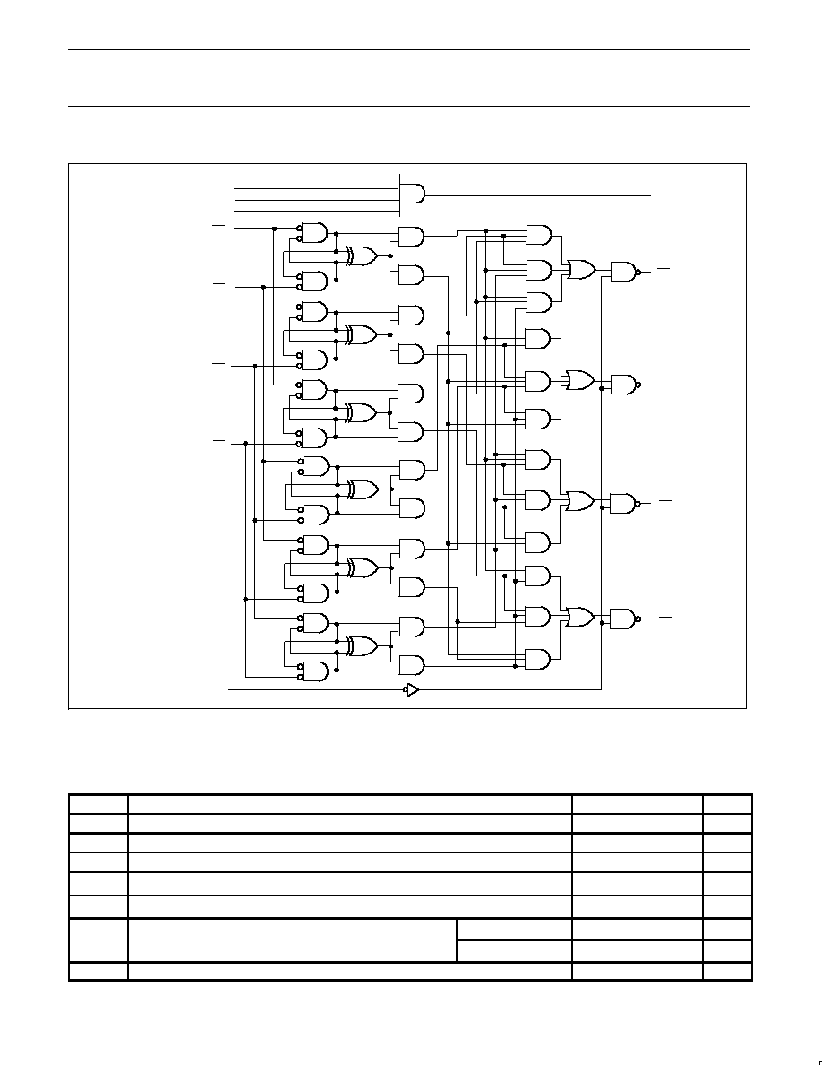
LOGIC DIAGRAM
BG0
13
V
CC
= Pin 16
GND = Pin 8
BR0
4
EN
15
14
YOUT
6
BR2
SF00444
1
2
3
5
7
BR3
BR1
10
11
12
BG3
BG2
BG1
A
B
C
D
ABSOLUTE MAXIMUM RATINGS
(Operation beyond the limit set forth in this table may impair the useful life of the device. Unless otherwise noted these limits are over the
operating free air temperature range.)
SYMBOL
PARAMETER
RATING
UNIT
V
CC
Supply voltage
≠0.5 to +7.0
V
V
IN
Input voltage
≠0.5 to +7.0
V
I
IN
Input current
≠30 to +5
mA
V
OUT
Voltage applied to output in high output state
≠0.5 to V
CC
V
I
OUT
Current applied to output in low output state
48
mA
T
amb
Operating free air temperature range
Commercial range
0 to +70
∞
C
Industrial range
≠40 to +85
∞
C
T
stg
Storage temperature range
≠65 to +150
∞
C

Philips Semiconductors
Product specification
74F786
4-bit asynchronous bus arbiter
February 14, 1991
6
RECOMMENDED OPERATING CONDITIONS
SYMBOL
PARAMETER
LIMITS
T
A
=
≠40 to
+85
∞
C
UNIT
MIN
NOM
MAX
V
CC
Supply voltage
4.5
5.0
5.5
V
V
IN
High≠level input voltage
2.0
V
V
IL
Low≠level input voltage
0.8
V
I
Ik
Input clamp current
≠18
mA
I
OH
High≠level output current
≠1
mA
I
OL
Low≠level output current
24
mA
T
amb
Operating free air temperature range
Commercial range
0
+70
∞
C
Industrial range
≠40
+85
∞
C
DC ELECTRICAL CHARACTERISTICS
(Over recommended operating free-air temperature range unless otherwise noted.)
SYMBOL
PARAMETER
TEST
LIMITS
UNIT
CONDITIONS
1
MIN
TYP
2
MAX
V
OH
High≠level output voltage
V
CC
= MIN, V
IL
=
MAX,
I
OH
= MAX
±
10%V
CC
2.4
V
V
IH
= MIN
±
5%V
CC
2.7
3.3
V
V
OL
Low≠level output voltage
V
CC
= MIN, V
IL
=
MAX,
I
OL
= MAX
±
10%V
CC
0.30
0.50
V
V
IH
= MIN
±
5%V
CC
0.30
0.50
V
V
IK
Input clamp voltage
V
CC
= MIN, I
I
= I
IK
-0.73
-1.2
V
I
I
Input current at maximum input voltage
V
CC
= 0.0V, V
I
= 7.0V
100
µ
A
I
IH
High≠level input current
V
CC
= MAX, V
I
= 2.7V
20
µ
A
I
IL
Low≠level input current
A ≠ D, EN
V
CC
= MAX, V
I
= 0.5V
-0.6
mA
BRn
-1.8
mA
I
OS
Short≠circuit output current
3
V
CC
= MAX
-60
-150
mA
I
CC
Supply current (total)
V
CC
= MAX
55
80
mA
Notes to DC electrical characteristics
1. For conditions shown as MIN or MAX, use the appropriate value specified under recommended operating conditions for the applicable type.
2. All typical values are at V
CC
= 5V, T
amb
= 25
∞
C.
3. Not more than one output should be shorted at a time. For testing I
OS
, the use of high-speed test apparatus and/or sample-and-hold
techniques are preferable in order to minimize internal heating and more accurately reflect operational values. Otherwise, prolonged shorting
of a high output may raise the chip temperature well above normal and thereby cause invalid readings in other parameter tests. In any
sequence of parameter tests, I
OS
tests should be performed last.
Philips Semiconductors
Product specification
74F786
4-bit asynchronous bus arbiter
February 14, 1991
7
AC ELECTRICAL CHARACTERISTICS
LIMITS
T
amb
= +25
∞
C
T
amb
= 0
∞
C to +70
∞
C
T
amb
= ≠40
∞
C to
+85
∞
C
SYM-
BOL
PARAMETER
TEST
V
CC
= +5.0V
V
CC
= +5.0V
±
10%
V
CC
= +5.0V
±
10%
UNIT
CONDITION
C
L
= 50pF,
R
L
= 500
C
L
= 50pF,
R
L
= 500
C
L
= 50pF,
R
L
= 500
MIN
TYP
MAX
MIN
MAX
MIN
MAX
t
PLH
t
PHL
Propagation delay,
A, B, C, D to YOUT
Waveform 1
2.5
2.5
4.5
4.5
7.5
7.5
2.0
2.5
8.5
7.5
2.0
2.5
8.5
7.5
ns
t
PLH
t
PHL
Propagation delay,
BRn to BGn
Waveform 2
5.0
4.5
7.0
6.5
10.0
9.5
4.5
4.0
10.5
10.0
4.5
4.0
10.5
10.0
ns
t
PLH
t
PHL
Propagation delay,
EN to BGn
Waveform 2
3.0
2.5
5.0
4.5
8.0
7.5
2.5
2.5
8.5
8.0
2.5
2.5
8.5
8.0
ns
t
PHL
Propagation delay,
BRa to BGb
Waveform 2
5.0
7.0
10.0
4.5
10.5
4.5
10.5
ns
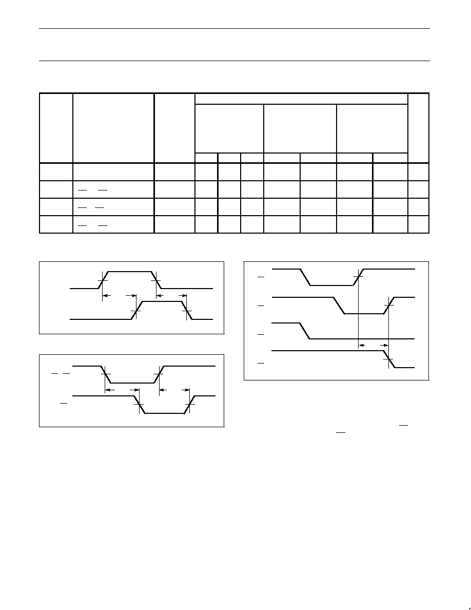
AC WAVEFORMS
V
M
V
M
V
M
V
M
A, B, C, D
YOUT
t
PLH
t
PHL
SF00445
Waveform 1. Propagation delay for AND gate to output
V
M
V
M
V
M
V
M
t
PHL
t
PLH
BRn, EN
BGn
SF00446
Waveform 2. Propagation delay for bus request or enable to
bus grant output
V
M
V
M
BRa
BGa
BRb
BGb
V
M
t
PHL
SF00447
Waveform 3. Propagation delay for bus request to bus grant
output
Notes to AC waveforms
1. For all waveforms, V
M
= 1.5V.
2. a and b represents any of the bus requests or grants. BGa
low≠to≠high transition and the BGb high≠to≠low transition occur
simultaneously.
Philips Semiconductors
Product specification
74F786
4-bit asynchronous bus arbiter
February 14, 1991
8
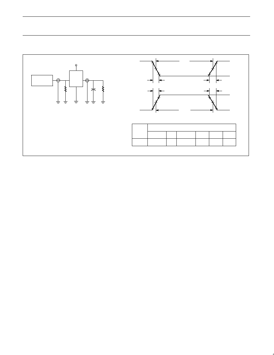
TEST CIRCUIT AND WAVEFORMS
tw
90%
VM
10%
90%
VM
10%
90%
VM
10%
90%
VM
10%
NEGATIVE
PULSE
POSITIVE
PULSE
tw
AMP (V)
0V
0V
tTHL (tf
)
INPUT PULSE REQUIREMENTS
rep. rate
t
w
t
TLH
t
THL
1MHz
500ns
2.5ns
2.5ns
Input Pulse Definition
VCC
family
74F
D.U.T.
PULSE
GENERATOR
RL
CL
RT
VIN
VOUT
Test Circuit for Totem-Pole Outputs
DEFINITIONS:
R
L
= Load resistor;
see AC ELECTRICAL CHARACTERISTICS for value.
C
L
= Load capacitance includes jig and probe capacitance;
see AC ELECTRICAL CHARACTERISTICS for value.
R
T
= Termination resistance should be equal to Z
OUT
of
pulse generators.
tTHL (tf
)
tTLH (tr
)
tTLH (tr
)
AMP (V)
amplitude
3.0V
1.5V
V
M
SF00006
Philips Semiconductors
Product specification
74F786
4-bit asynchronous bus arbiter
1991 Feb 14
9
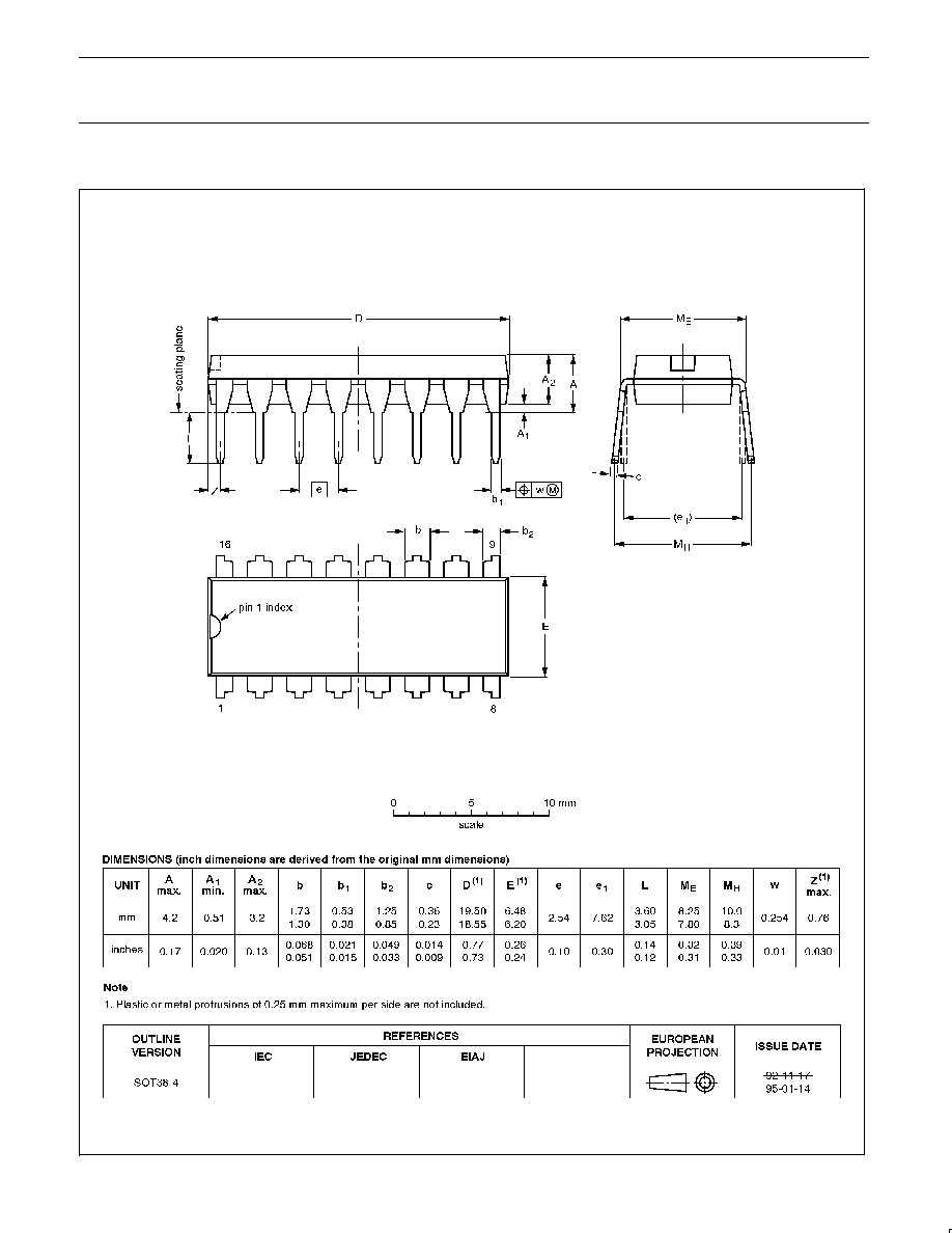
DIP16:
plastic dual in-line package; 16 leads (300 mil)
SOT38-4

Philips Semiconductors
Product specification
74F786
4-bit asynchronous bus arbiter
1991 Feb 14
10
SO16:
plastic small outline package; 16 leads; body width 3.9 mm
SOT109-1

Philips Semiconductors
Product specification
74F786
4-bit asynchronous bus arbiter
1991 Feb 14
11
NOTES

Philips Semiconductors
Product specification
74F786
4-bit asynchronous bus arbiter
yyyy mmm dd
12
Definitions
Short-form specification -- The data in a short-form specification is extracted from a full data sheet with the same type number and title. For
detailed information see the relevant data sheet or data handbook.
Limiting values definition -- Limiting values given are in accordance with the Absolute Maximum Rating System (IEC 134). Stress above one
or more of the limiting values may cause permanent damage to the device. These are stress ratings only and operation of the device at these or
at any other conditions above those given in the Characteristics sections of the specification is not implied. Exposure to limiting values for extended
periods may affect device reliability.
Application information -- Applications that are described herein for any of these products are for illustrative purposes only. Philips
Semiconductors make no representation or warranty that such applications will be suitable for the specified use without further testing or
modification.
Disclaimers
Life support -- These products are not designed for use in life support appliances, devices or systems where malfunction of these products can
reasonably be expected to result in personal injury. Philips Semiconductors customers using or selling these products for use in such applications
do so at their own risk and agree to fully indemnify Philips Semiconductors for any damages resulting from such application.
Right to make changes -- Philips Semiconductors reserves the right to make changes, without notice, in the products, including circuits, standard
cells, and/or software, described or contained herein in order to improve design and/or performance. Philips Semiconductors assumes no
responsibility or liability for the use of any of these products, conveys no license or title under any patent, copyright, or mask work right to these
products, and makes no representations or warranties that these products are free from patent, copyright, or mask work right infringement, unless
otherwise specified.
Philips Semiconductors
811 East Arques Avenue
P.O. Box 3409
Sunnyvale, California 94088≠3409
Telephone 800-234-7381
©
Copyright Philips Electronics North America Corporation 1998
All rights reserved. Printed in U.S.A.
print code
Date of release: 10-98
Document order number:
9397-750-05181
Philips
Semiconductors
Data sheet
status
Objective
specification
Preliminary
specification
Product
specification
Product
status
Development
Qualification
Production
Definition
[1]
This data sheet contains the design target or goal specifications for product development.
Specification may change in any manner without notice.
This data sheet contains preliminary data, and supplementary data will be published at a later date.
Philips Semiconductors reserves the right to make chages at any time without notice in order to
improve design and supply the best possible product.
This data sheet contains final specifications. Philips Semiconductors reserves the right to make
changes at any time without notice in order to improve design and supply the best possible product.
Data sheet status
[1]
Please consult the most recently issued datasheet before initiating or completing a design.