 | –≠–ª–µ–∫—Ç—Ä–æ–Ω–Ω—ã–π –∫–æ–º–ø–æ–Ω–µ–Ω—Ç: N74F828D | –°–∫–∞—á–∞—Ç—å:  PDF PDF  ZIP ZIP |

Philips Semiconductors
74F827
10-bit buffer/line driver, non-inverting
(3-State)
74F828
10-bit buffer/line driver, inverting
(3-State)
Product specification
1994 Dec 5
INTEGRATED CIRCUITS
IC15 Data Handbook
Philips Semiconductors
Product specification
74F827, 74F828
Buffers
74F827 10-bit buffer/line driver, non-inverting (3-State)
74F828 10-bit buffer/line driver, inverting (3-State)
2
1994 Dec 05
853-0880 14382
FEATURES
∑
High impedance NPN base inputs for reduced loading (20
µ
A in
High and Low states)
∑
I
IL
is 20
µ
A vs FAST family spec of 600
µ
A and 1000
µ
A for
AMD 29827/29828 series
∑
Ideal where high speed, light bus loading and increased fan-in are
required
∑
Controlled rise and fall times to minimize ground bounce
∑
Glitch free power-up in 3-State
∑
Flow through pinout architecture for microprocessor oriented
applications
∑
Outputs sink 64mA
∑
74F827 available in SSOP type II package
DESCRIPTION
The 74F827 and 74F828 10-Bit buffers provide high performance
bus interface buffering for wide data/address paths or buses
carrying parity. They have NOR Output Enables (OE0, OE1) for
maximum control flexibility.
The 74F827 and 74F828 are functionally and pin compatible to AMD
AM29827 and AM29828. The 74F828 is an inverting version of
74F827.
TYPE
TYPICAL PROPAGATION
DELAY
TYPICAL SUPPLY
CURRENT
(TOTAL)
74F827
6.0ns
60mA
74F828
6.0ns
55mA
ORDERING INFORMATION
PACKAGES
COMMERCIAL RANGE
V
CC
= 5V
"
10%; T
A
= 0
∞
C to +70
∞
C
DRAWING NUMBER
24-Pin Plastic DIP (300 mil)
N74F827N, N74F828N
SOT222-1
24-Pin Plastic SOL
N74F827D, N74F828D
SOT137-1
24-Pin Plastic SSOP Type II
N74F827DB
SOT340-1
INPUT AND OUTPUT LOADING AND FAN-OUT TABLE
PINS
DESCRIPTION
74F(U.L.)
HIGH/LOW
LOAD VALUE
HIGH/LOW
D0-D9
Data inputs
1.0/0.033
20
µ
A/20
µ
A
OE0-OE1
Output enable inputs (active Low)
1.0/0.033
20
µ
A/20
µ
A
Q0-Q9
Data outputs (74F827)
1200/106.7
24mA/64mA
Q0-Q9
Data outputs ( 74F828)
1200/106.7
24mA/64mA
NOTES:
One (1.0) FAST Unit Load is defined as: 20
µ
A in the High state and 0.6 mA in the Low state.

Philips Semiconductors
Product specification
74F827, 74F828
Buffers
1994 Dec 05
3
PIN CONFIGURATION - 74F827
SF00266
1
2
3
4
5
6
7
8
9
10
11
12
13
14
15
16
17
18
19
20
21
22
23
24
OE0
D0
D1
D2
D3
D4
D5
D6
D7
D8
D9
VCC
Q0
Q1
Q2
Q3
Q4
Q5
Q7
Q6
Q8
Q9
OE1
GND
LOGIC SYMBOL - 74F827
1
13
OE0
OE1
2
3
4
5
6
7
8
9
10
11
D0 D1 D2 D3 D4 D5 D6 D7 D8 D9
Q0 Q1 Q2 Q3 Q4 Q5 Q6 Q7 Q8 Q9
23 22 21 20 19 18 17 16 15 14
V
CC
= Pin 24
GND = Pin 12
SF00267
LOGIC SYMBOL (IEEE/IEC) - 74F827
2
23
3
22
4
21
5
20
6
19
7
18
8
17
9
16
13
&
1
10
15
11
14
EN1
1
SF00268
PIN CONFIGURATION - 74F828
SF00269
1
2
3
4
5
6
7
8
9
10
11
12
13
14
15
16
17
18
19
20
21
22
23
24
OE0
D0
D1
D2
D3
D4
D5
D6
D7
D8
D9
VCC
Q0
Q1
Q2
Q3
Q4
Q5
Q7
Q6
Q8
Q9
OE1
GND
LOGIC SYMBOL - 74F828
1
13
OE0
OE1
2
3
4
5
6
7
8
9
10
11
D0 D1 D2 D3 D4 D5 D6 D7 D8 D9
Q0 Q1 Q2 Q3 Q4 Q5 Q6 Q7 Q8 Q9
23 22 21 20 19 18 17 16 15 14
V
CC
= Pin 24
GND = Pin 12
SF00270
LOGIC SYMBOL (IEEE/IEC) - 74F828
2
23
3
22
4
21
5
20
6
19
7
18
8
17
9
16
13
&
1
10
15
11
14
EN1
1
SF00271
Philips Semiconductors
Product specification
74F827, 74F828
Buffers
1994 Dec 05
4
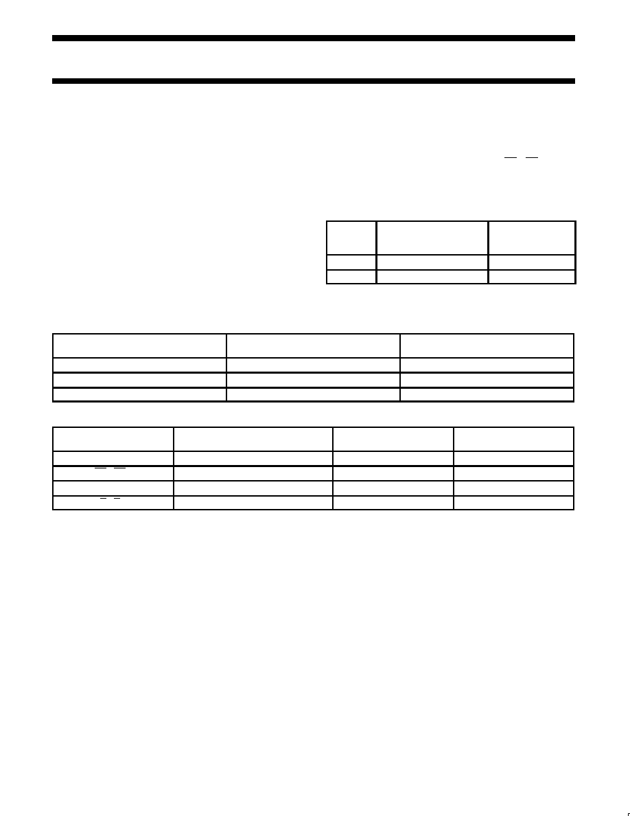
LOGIC DIAGRAM 74F827
2
D0
Q0
23
1
OE0
3
D1
Q1
22
4
D2
Q2
21
5
D3
Q3
20
6
D4
Q4
19
7
D5
Q5
18
8
D6
Q6
17
9
D7
Q7
16
10
D8
Q8
15
11
D9
Q9
14
13
OE1
V
CC
= Pin 24
GND = Pin 12
SF00272
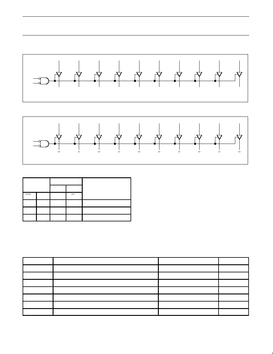
LOGIC DIAGRAM 74F828
2
D0
Q0
23
1
OE0
3
D1
Q1
22
4
D2
Q2
21
5
D3
Q3
20
6
D4
Q4
19
7
D5
Q5
18
8
D6
Q6
17
9
D7
Q7
16
10
D8
Q8
15
11
D9
Q9
14
13
OE1
V
CC
= Pin 24
GND = Pin 12
SF00280
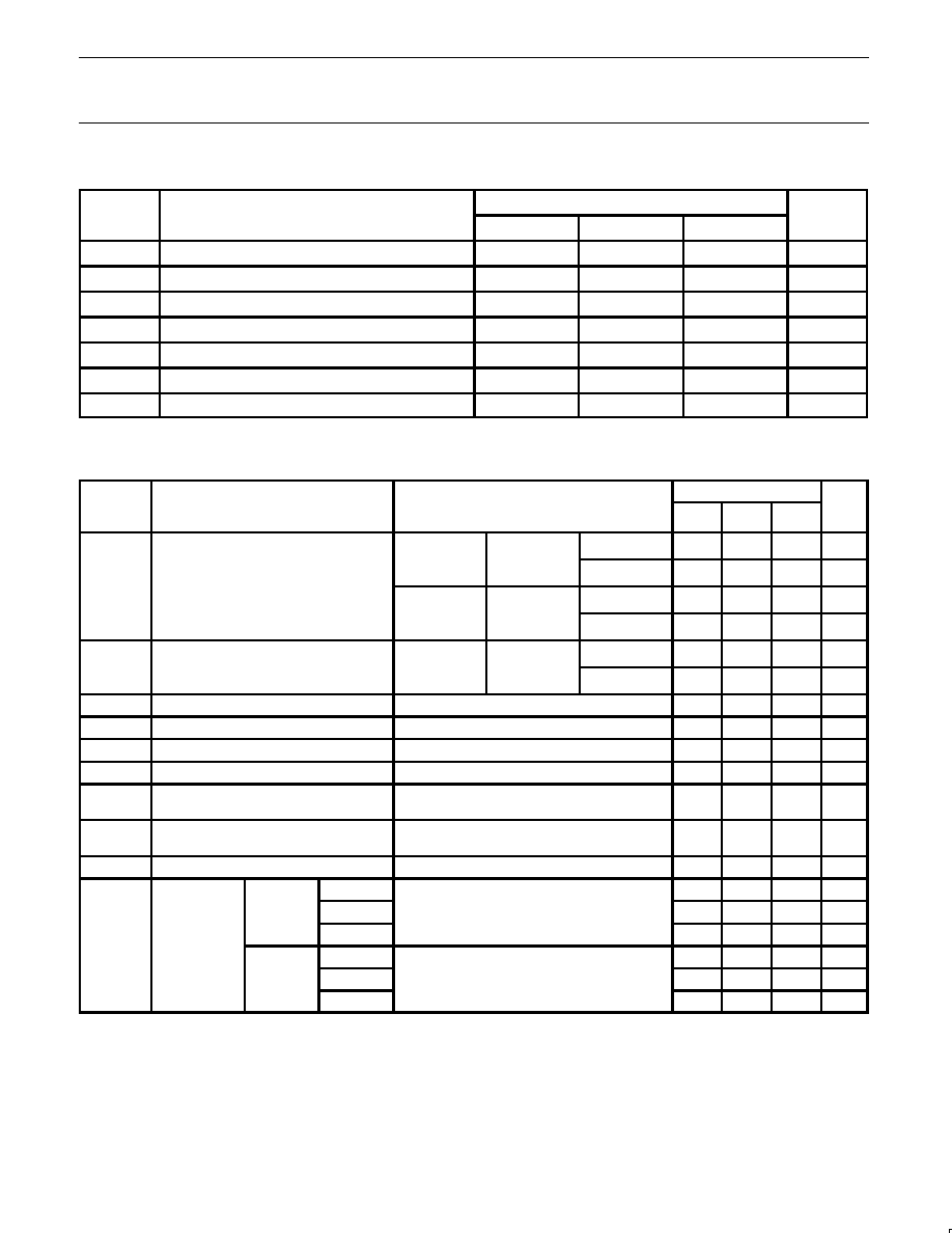
FUNCTION TABLE
INPUTS
OUTPUTS
INPUTS
74F827
74F828
OPERATING MODE
OEn
Dn
Qn
Qn
L
L
L
H
Transparent
L
H
H
L
Transparent
H
X
Z
Z
High impedance
H = High voltage level
L
= Low voltage level
X = Don't care
Z = High impedance "off" state
ABSOLUTE MAXIMUM RATINGS
Operation beyond the limits set forth in this table may impair the useful life of the device. Unless otherwise noted these limits are over the
operating free-air temperature range.
SYMBOL
PARAMETER
RATING
UNIT
V
CC
Supply voltage
≠0.5 to +7.0
V
V
IN
Input voltage
≠0.5 to +7.0
V
I
IN
Input current
≠30 to +5
mA
V
OUT
Voltage applied to output in High output state
≠0.5 to +V
CC
V
I
OUT
Current applied to output in Low output state
128
mA
T
A
Operating free-air temperature range
0 to + 70
∞
C
T
stg
Storage temperature range
≠65 to + 150
∞
C
Philips Semiconductors
Product specification
74F827, 74F828
Buffers
1994 Dec 05
5
RECOMMENDED OPERATING CONDITIONS
SYMBOL
PARAMETER
LIMITS
UNIT
SYMBOL
PARAMETER
Min
Nom
Max
UNIT
V
CC
Supply voltage
4.5
5.0
5.5
V
V
IH
High-level input voltage
2.0
V
V
IL
Low-level input voltage
0.8
V
I
IK
Input clamp current
≠18
mA
I
OH
High-level output current
≠24
mA
I
OL
Low-level output current
64
mA
T
amb
Operating free-air temperature range
0
+70
∞
C
DC ELECTRICAL CHARACTERISTICS
Over recommended operating free-air temperature range unless otherwise noted.
SYMBOL
PARAMETER
TEST CONDITIONS
1
LIMITS
UNIT
SYMBOL
PARAMETER
TEST CONDITIONS
1
MIN
TYP
2
MAX
UNIT
SYMBOL
PARAMETER
TEST CONDITIONS
MIN
TYP
2
MAX
UNIT
MIN
TYP
MAX
V
CC
= MIN,
V
IL
= MAX
I
OH
= ≠15mA
"
10%V
CC
2.4
V
V
OH
High-level output voltage
V
IL
= MAX,
V
IH
= MIN
I
OH
= ≠15mA
"
5%V
CC
2.4
3.3
V
V
OH
High-level out ut voltage
V
CC
= MIN,
V
IL
= MAX
I
OH
= ≠24mA
"
10%V
CC
2.0
V
V
IL
= MAX,
V
IH
= MIN
I
OH
= ≠24mA
"
5%V
CC
2.0
V
V
OL
Low-level output voltage
V
CC
= MIN,
V
IL
= MAX,
I
OL
MAX
"
10%V
CC
0.55
V
V
OL
Low-level out ut voltage
V
IL
= MAX,
V
IH
= MIN
I
OL = MAX
"
5%V
CC
0.42
0.55
V
V
IK
Input clamp voltage
V
CC
= MIN, I
I
= I
IK
≠0.73
≠1.2
V
I
I
Input current at maximum input voltage
V
CC
= 0.0V, V
I
= 7.0V
100
µ
A
I
IH
High-level input current
V
CC
= MAX, V
I
= 2.7V
20
µ
A
I
IL
Low-level input current
V
CC
= MAX, V
I
= 0.5V
≠20
µ
A
I
OZH
Off-state output current,
High voltage applied
V
CC
= MAX, V
O
= 2.7V
50
µ
A
I
OZL
Off-state output current,
Low voltage applied
V
CC
= MAX, V
O
= 0.5V
≠50
µ
A
I
OS
Short circuit output current
3
V
CC
= MAX
≠100
≠225
mA
I
CCH
50
70
mA
74F827
I
CCL
V
CC
= MAX
70
100
mA
I
CC
Supply current
I
CCZ
60
90
mA
I
CC
y
(total)
I
CCH
30
45
mA
74F828
I
CCL
V
CC
= MAX
65
85
mA
I
CCZ
55
70
mA
NOTES:
1. For conditions shown as MIN or MAX, use the appropriate value specified under operating conditions for the applicable type.
2. All typical values are at V
CC
= 5V, T
A
= 25
∞
C.
3. Not more than one output should be shorted at one time. For testing I
OS
, the use of high-speed test apparatus and/or sample-and-hold
techniques are preferable in order to minimize internal heating and more accurately reflect operational values. Otherwise, prolonged shorting
of a High output may raise the chip temperature well above normal and thereby cause invalid readings in other parameter tests. In any
sequence of parameter tests, I
OS
tests should be performed last.
Philips Semiconductors
Product specification
74F827, 74F828
Buffers
1994 Dec 05
6
AC CHARACTERISTICS
LIMITS
SYMBOL
PARAMETER
T
amb
= +25
∞
C
V
CC
= 5V
C
L
= 50pF
R
L
= 500
T
amb
= 0
∞
C to +70
∞
C
V
CC
= 5V
"
10%
C
L
= 50pF
R
L
= 500
UNIT
Min
Typ
Max
Min
Max
t
PLH
t
PHL
Propagation delay
D
n
to Q
n
Waveform 1
2.0
2.0
5.5
4.5
8.5
8.5
2.0
2.0
9.0
9.0
ns
t
PZH
t
PZL
Output enable time
OE
n
to Q
n
74F827
Waveform 3
Waveform 4
5.0
4.0
8.0
6.0
12.0
10.5
4.5
4.0
14.0
11.5
ns
t
PHZ
t
PLZ
Output disable time
OE
n
to Q
n
Waveform 3
Waveform 4
2.5
2.5
5.0
5.0
8.0
8.0
2.0
2.0
8.5
8.5
ns
t
PLH
t
PHL
Propagation delay
D
n
to Q
n
Waveform 2
2.0
1.0
6.0
3.0
8.5
7.0
2.0
1.0
9.5
8.0
ns
t
PZH
t
PZL
Output enable time
OE
n
to Q
n
74F828
Waveform 3
Waveform 4
6.0
5.0
8.0
7.0
11.5
10.5
5.5
4.5
14.0
12.0
ns
t
PHZ
t
PLZ
Output disable time
OE
n
to Q
n
Waveform 3
Waveform 4
2.5
1.5
5.0
4.0
8.5
7.0
2.0
1.5
9.0
8.0
ns
AC CHARACTERISTICS
for 1 Output switching with C
L
= 300pF and R
L
= 500
load
LIMITS
SYMBOL
PARAMETER
T
amb
= +25
∞
C
V
CC
= 5V
C
L
= 300pF
R
L
= 500
T
amb
= 0
∞
C to +70
∞
C
V
CC
= 5V
"
10%
C
L
= 300pF
R
L
= 500
UNIT
MIN
Typ
Max
MIN
Max
t
PLH
t
PHL
Propagation delay
D
n
to Q
n
Waveform 1
9.5
7.5
13.0
10.0
14.0
11.0
ns
t
PZH
t
PZL
Output enable time
OE
n
to Q
n
74F827
Waveform 3
Waveform 4
15.0
9.5
20.0
13.0
21.0
14.0
ns
t
PHZ
t
PLZ
Output disable time
OE
n
to Q
n
Waveform 3
Waveform 4
15.0
9.5
19.0
13.5
20.0
14.0
ns
t
PLH
t
PHL
Propagation delay
D
n
to Q
n
Waveform 2
10.0
6.0
13.0
9.0
14.0
10.0
ns
t
PZH
t
PZL
Output enable time
OE
n
to Q
n
74F828
Waveform 3
Waveform 4
15.5
10.5
19.0
13.0
21.0
14.0
ns
t
PHZ
t
PLZ
Output disable time
OE
n
to Q
n
Waveform 3
Waveform 4
15.0
10.0
18.0
13.0
20.0
14.5
ns

Philips Semiconductors
Product specification
74F827, 74F828
Buffers
1994 Dec 05
7
AC CHARACTERISTICS
for 10 Outputs switching with C
L
= 300pF and R
L
= 500
load
LIMITS
SYMBOL
PARAMETER
T
amb
= +25
∞
C
V
CC
= 5V
C
L
= 50pF
R
L
= 500
T
amb
= 0
∞
C to +70
∞
C
V
CC
= 5V
"
10%
C
L
= 50pF
R
L
= 500
UNIT
MIN
Typ
Max
MIN
Max
t
PLH
t
PHL
Propagation delay
D
n
to Q
n
Waveform 1
12.0
14.0
16.0
17.0
17.0
18.0
ns
t
PZH
t
PZL
Output enable time
OE
n
to Q
n
74F827
Waveform 3
Waveform 4
15.0
17.0
20.0
21.0
21.0
21.5
ns
t
PHZ
t
PLZ
Output disable time
OE
n
to Q
n
Waveform 3
Waveform 4
15.0
12.5
19.0
15.5
20.0
16.0
ns
t
PLH
t
PHL
Propagation delay
D
n
to Q
n
Waveform 2
10.0
10.0
17.0
13.5
18.0
14.0
ns
t
PZH
t
PZL
Output enable time
OE
n
to Q
n
74F828
Waveform 3
Waveform 4
18.0
15.0
21.0
18.0
23.0
19.0
ns
t
PHZ
t
PLZ
Output disable time
OE
n
to Q
n
Waveform 3
Waveform 4
16.5
11.5
19.5
14.5
22.5
15.0
ns
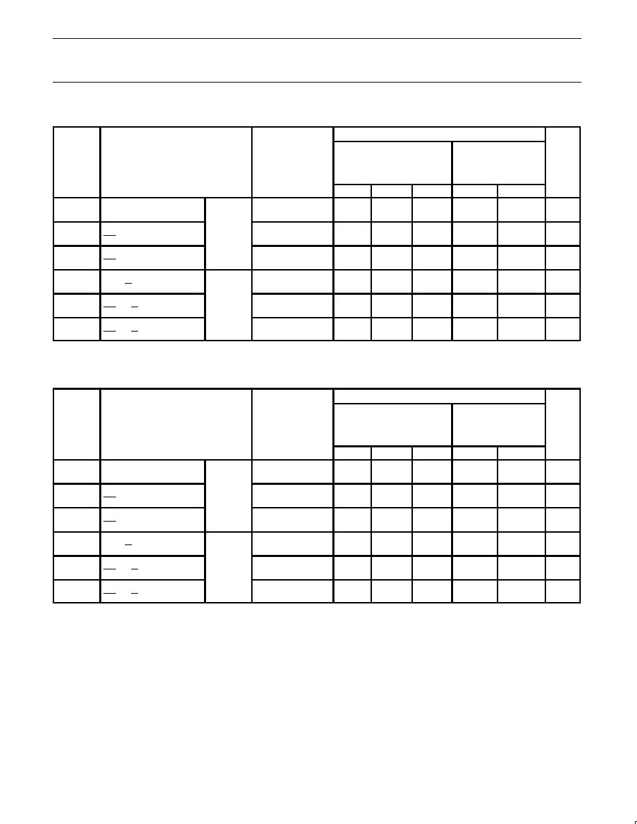
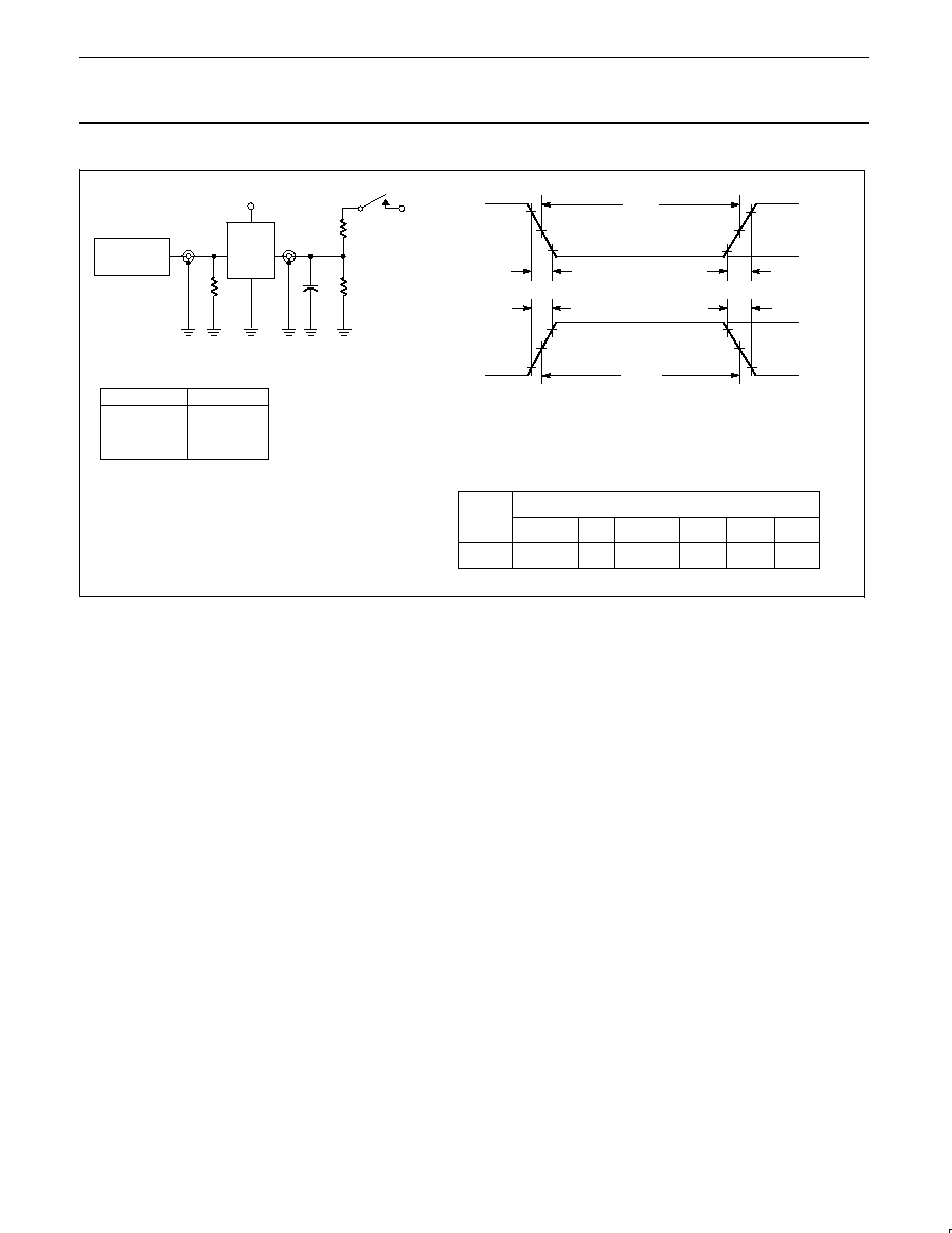
AC WAVEFORMS
For all waveforms, V
M
= 1.5V
VM
VM
VM
VM
Qn
Dn
tPLH
tPHL
SF00125
Waveform 1. Propagation Delay for Non-Inverting Output
VM
VM
VM
VM
Qn
Dn
tPHL
tPLH
SF00282
Waveform 2. Propagation Delay for Inverting Output
Qn, Qn
VM
VM
VM
tPHZ
tPZH
OEn
VOH -0.3V
0V
SF00263
Waveform 3. 3-State Output Enable Time to High Level
and Output Disable Time from High Level
VM
VM
VM
tPLZ
tPZL
VOL +0.3V
OEn
Qn, Qn
SF00264
Waveform 4. 3-State Output Enable Time to Low Level
and Output Disable Time from Low Level
Philips Semiconductors
Product specification
74F827, 74F828
Buffers
1994 Dec 05
8
tw
90%
VM
10%
90%
VM
10%
90%
VM
10%
90%
VM
10%
NEGATIVE
PULSE
POSITIVE
PULSE
tw
AMP (V)
0V
0V
tTHL (tf
)
INPUT PULSE REQUIREMENTS
rep. rate
t
w
t
TLH
t
THL
1MHz
500ns
2.5ns
2.5ns
Input Pulse Definition
VCC
family
74F
D.U.T.
PULSE
GENERATOR
RL
CL
RT
VIN
VOUT
Test Circuit for Open Collector Outputs
DEFINITIONS:
R
L
= Load resistor;
see AC electrical characteristics for value.
C
L
= Load capacitance includes jig and probe capacitance;
see AC electrical characteristics for value.
R
T
= Termination resistance should be equal to Z
OUT
of
pulse generators.
tTHL (tf
)
tTLH (tr
)
tTLH (tr
)
AMP (V)
amplitude
3.0V
1.5V
V
M
RL
7.0V
SF00128
TEST
SWITCH
t
PLZ
closed
t
PZL
closed
All other
open
SWITCH POSITION
Philips Semiconductors
Product specification
74F827, 74F828
Buffers
1994 Dec 05
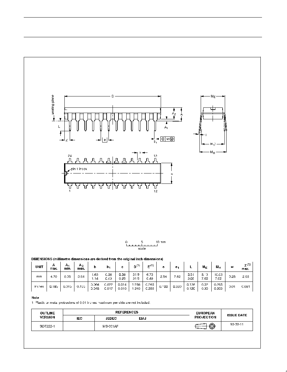
9
DIP24:
plastic dual in-line package; 24 leads (300 mil)
SOT222-1
Philips Semiconductors
Product specification
74F827, 74F828
Buffers
1994 Dec 05
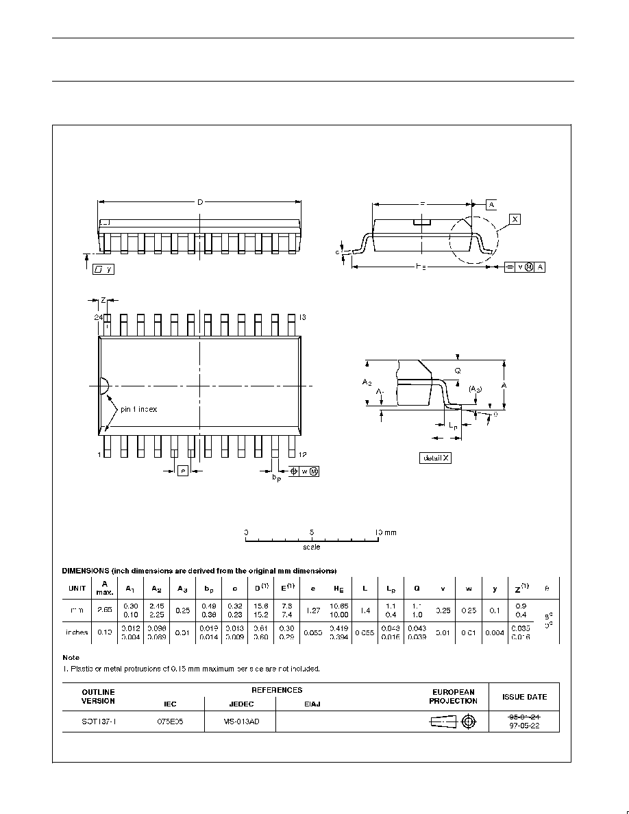
10
SO24:
plastic small outline package; 24 leads; body width 7.5 mm
SOT137-1
Philips Semiconductors
Product specification
74F827, 74F828
Buffers
1994 Dec 05
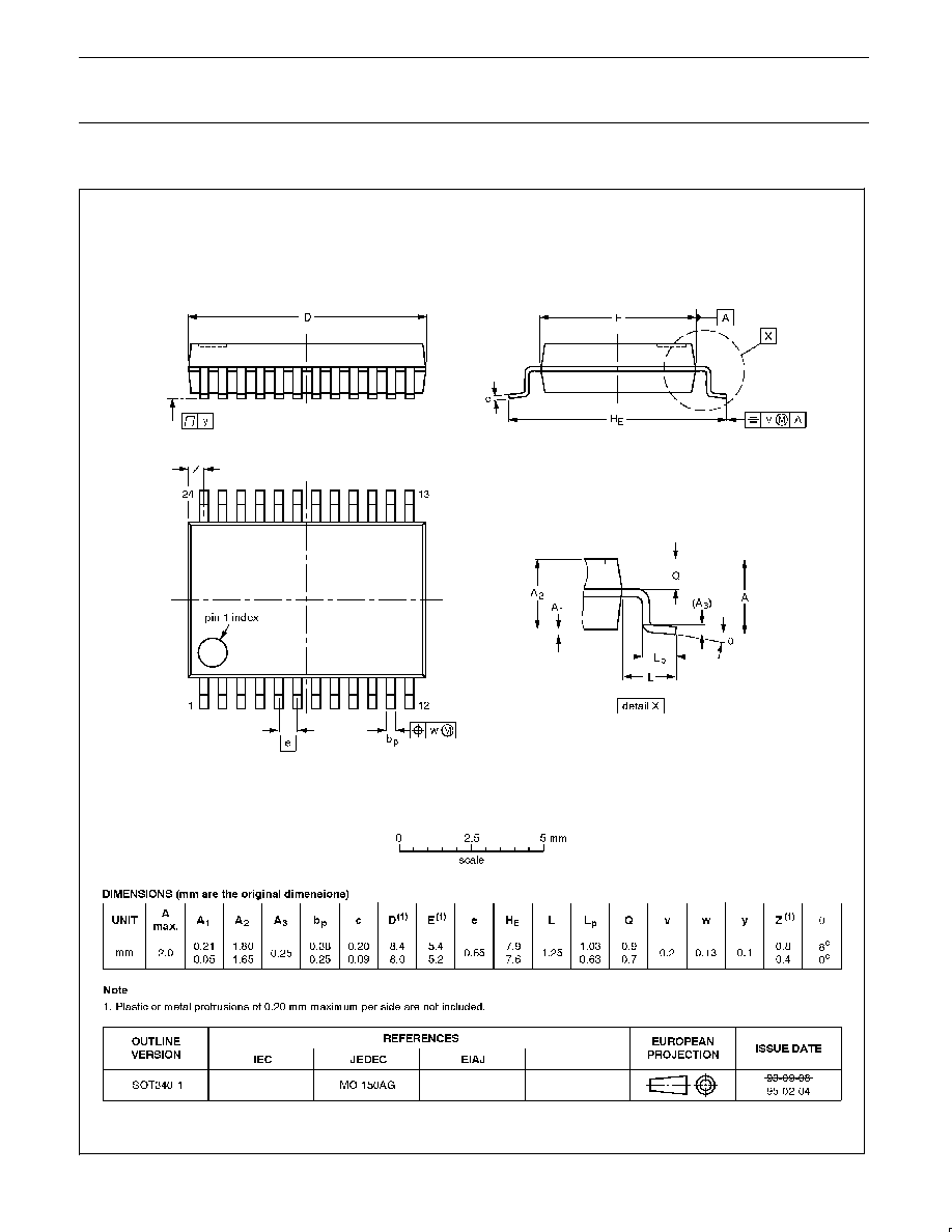
11
SSOP24:
plastic shrink small outline package; 24 leads; body width 5.3 mm
SOT340-1
Philips Semiconductors
Product specification
74F827, 74F828
Buffers
Philips Semiconductors and Philips Electronics North America Corporation reserve the right to make changes, without notice, in the products,
including circuits, standard cells, and/or software, described or contained herein in order to improve design and/or performance. Philips
Semiconductors assumes no responsibility or liability for the use of any of these products, conveys no license or title under any patent, copyright,
or mask work right to these products, and makes no representations or warranties that these products are free from patent, copyright, or mask
work right infringement, unless otherwise specified. Applications that are described herein for any of these products are for illustrative purposes
only. Philips Semiconductors makes no representation or warranty that such applications will be suitable for the specified use without further testing
or modification.
LIFE SUPPORT APPLICATIONS
Philips Semiconductors and Philips Electronics North America Corporation Products are not designed for use in life support appliances, devices,
or systems where malfunction of a Philips Semiconductors and Philips Electronics North America Corporation Product can reasonably be expected
to result in a personal injury. Philips Semiconductors and Philips Electronics North America Corporation customers using or selling Philips
Semiconductors and Philips Electronics North America Corporation Products for use in such applications do so at their own risk and agree to fully
indemnify Philips Semiconductors and Philips Electronics North America Corporation for any damages resulting from such improper use or sale.
This data sheet contains preliminary data, and supplementary data will be published at a later date. Philips
Semiconductors reserves the right to make changes at any time without notice in order to improve design
and supply the best possible product.
Philips Semiconductors
811 East Arques Avenue
P.O. Box 3409
Sunnyvale, California 94088≠3409
Telephone 800-234-7381
DEFINITIONS
Data Sheet Identification
Product Status
Definition
Objective Specification
Preliminary Specification
Product Specification
Formative or in Design
Preproduction Product
Full Production
This data sheet contains the design target or goal specifications for product development. Specifications
may change in any manner without notice.
This data sheet contains Final Specifications. Philips Semiconductors reserves the right to make changes
at any time without notice, in order to improve design and supply the best possible product.
Philips Semiconductors and Philips Electronics North America Corporation
register eligible circuits under the Semiconductor Chip Protection Act.
©
Copyright Philips Electronics North America Corporation 1994
All rights reserved. Printed in U.S.A.