 | –≠–ª–µ–∫—Ç—Ä–æ–Ω–Ω—ã–π –∫–æ–º–ø–æ–Ω–µ–Ω—Ç: N74F85N | –°–∫–∞—á–∞—Ç—å:  PDF PDF  ZIP ZIP |

Philips Semiconductors
74F85
4-bit magnitude comparator
Product specification
1994 Sep 27
INTEGRATED CIRCUITS
IC15 Data Handbook
Philips Semiconductors
Product specification
74F85
4-bit magnitude comparator
2
September 27, 1994
853≠0055 13903
FEATURES
∑
High-impedance NPN base inputs for reduced loading
(20
µ
A in High and Low states)
∑
Magnitude comparison of any binary words
∑
Serial or parallel expansion without extra gating
DESCRIPTION
The 74F85 is a 4-bit magnitude comparator that can be expanded to
almost any length. It compares two 4-bit binary, BCD, or other
monotonic codes and presents the three possible magnitude results
at the outputs. The 4-bit inputs are weighted (A0≠A3) and (B0≠B3)
where A3 and B3 are the most significant bits. The operation of the
74F85 is described in the Function Table, showing all possible logic
conditions. The upper part of the table describes the normal
operation under all conditions that will occur in a single device or in
a series expansion scheme. In the upper part of the table the three
outputs are mutually exclusive. In the lower part of the table, the
outputs reflect the feed-forward conditions that exist in the parallel
expansion scheme. The expansion inputs I
A>B
, and I
A=B
and I
A<B
are the least significant bit positions. When used for series
expansion, the A>B, A=B and A<B outputs of the lease significant
word are connected to the corresponding I
A>B
, I
A=B
and I
A<B
inputs
of the next higher stage. Stages can be added in this manner to any
length, but a propagation delay penalty of about 15ns is added with
each additional stage. For proper operation, the expansion inputs of
the least significant word should be tied as follows: I
A>B
= Low,
I
A=B
= High, and I
A<B
= Low.
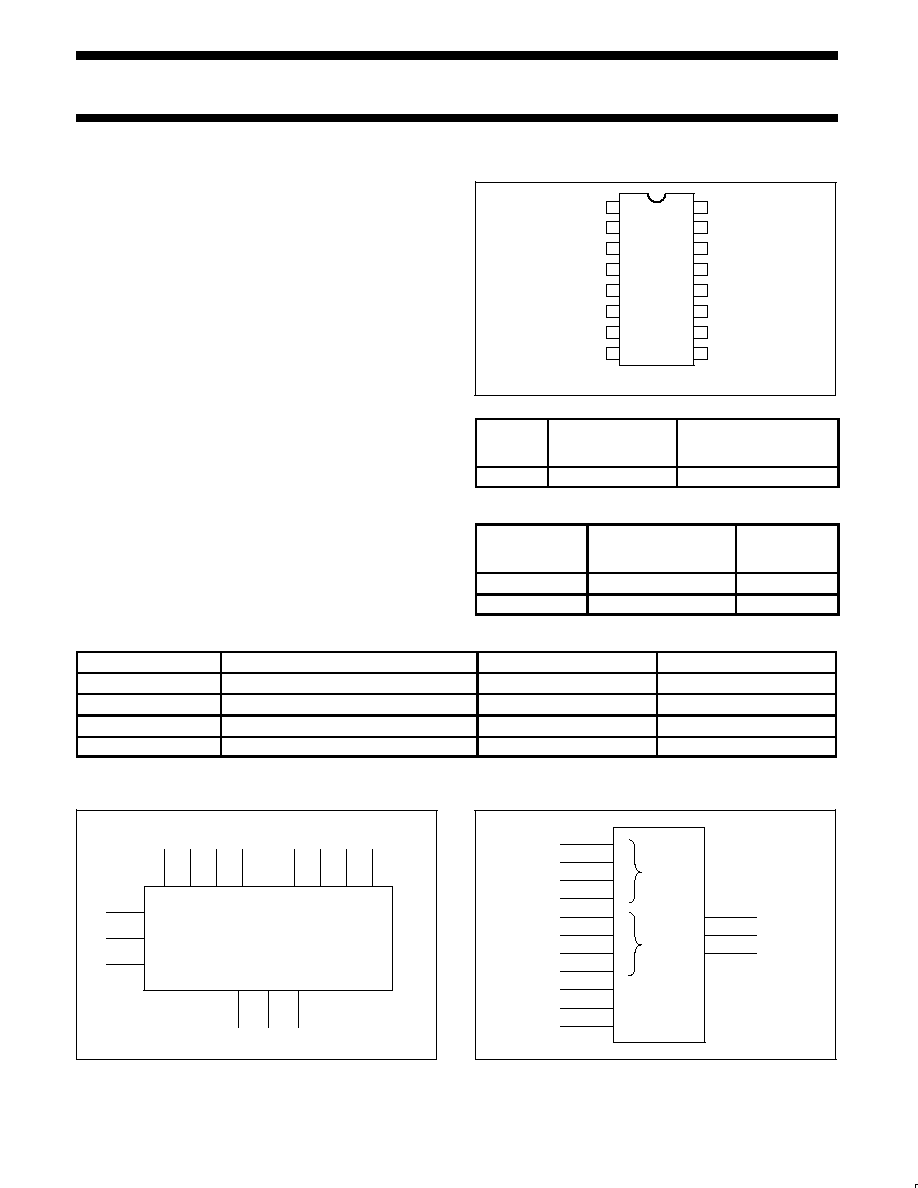
PIN CONFIGURATION
16
15
14
13
12
11
10
7
6
5
4
3
2
1
A<B
V
CC
A1
B1
A0
A2
A3
B2
B3
IA<B
A=B
IA=B
IA>B
A>B
9
8
GND
B0
SF00075
TYPE
TYPICAL
PROPAGATION
DELAY
TYPICAL
SUPPLY CURRENT
(TOTAL)
74F85
7.0ns
40mA
ORDERING INFORMATION
DESCRIPTION
COMMERCIAL RANGE
V
CC
= 5V
±
10%,
T
amb
= 0
∞
C to +70
∞
C
PKG DWG #
16-pin plastic DIP
N74F85N
SOT38-4
16-pin plastic SO
N74F85D
SOT162-1
INPUT AND OUTPUT LOADING AND FAN OUT TABLE
PINS
DESCRIPTION
74F (U.L.) HIGH/LOW
LOAD VALUE HIGH/LOW
A0≠A3
Comparing inputs
1.0/0.033
20
µ
A/20
µ
A
B0≠B3
Comparing inputs
1.0/0.033
20
µ
A/20
µ
A
I
A<B
, I
A=B
, I
A>B
Expansion inputs (active High)
1.0/0.033
20
µ
A/20
µ
A
A<B, A=B, A>B
Data outputs (active High)
50/33
1.0mA/20mA
NOTE: One (1.0) FAST unit load is defined as: 20
µ
A in the High state and 0.6mA in the Low state.
LOGIC SYMBOL
5
6
7
10
12
13
15
9
11
14
V
CC
= Pin 16
GND = Pin 8
SF00076
1
A0
A1
A2
A3
B0
B1
B2
B3
A>B
A=B
A<B
IA>B
IA=B
IA<B
2
3
4
IEC/IEEE SYMBOL
SF00077
COMP
7
6
5
10
12
13
15
9
11
14
1
2
3
4
0
3
0
3
<
=
>
P<Q
P=Q
P>Q
P
Q
Philips Semiconductors
Product specification
74F85
4-bit magnitude comparator
September 27, 1994
3
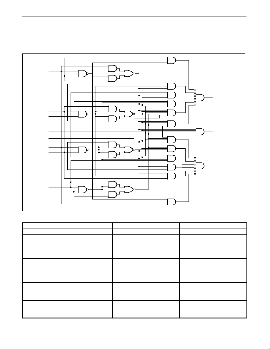
LOGIC DIAGRAM
5
6
7
A>B
A=B
A<B
V
CC
= Pin 16
GND = Pin 8
15
1
13
14
2
3
4
12
11
10
9
A3
B3
A2
B2
IA<B
IA=B
IA>B
A1
B1
A0
B0
SF00078
FUNCTION TABLE
COMPARING INPUTS
EXPANSION INPUTS
OUTPUTS
A3,B3
A2,B2
A1,B1
A0,B0
I
A>B
I
A<B
I
A=B
A>B
A<B
A=B
A3>B3
X
X
X
X
X
X
H
L
L
A3<B3
X
X
X
X
X
X
L
H
L
A3=B3
A2>B2
X
X
X
X
X
H
L
L
A3=B3
A2<B2
X
X
X
X
X
L
H
L
A3=B3
A2=B2
A1>B1
X
X
X
X
H
L
L
A3=B3
A2=B2
A1<B1
X
X
X
X
L
H
L
A3=B3
A2=B2
A1=B1
A0>B0
X
X
X
H
L
L
A3=B3
A2=B2
A1=B1
A0<B0
X
X
X
L
H
L
A3=B3
A2=B2
A1=B1
A0=B0
H
L
L
H
L
L
A3=B3
A2=B2
A1=B1
A0=B0
L
H
L
L
H
L
A3=B3
A2=B2
A1=B1
A0=B0
L
L
H
L
L
H
A3=B3
A2=B2
A1=B1
A0=B0
X
X
H
L
L
H
A3=B3
A2=B2
A1=B1
A0=B0
H
H
L
L
L
L
A3=B3
A2=B2
A1=B1
A0=B0
L
L
L
H
H
L
H = High voltage level
L = Low voltage level
X = Don't care
Philips Semiconductors
Product specification
74F85
4-bit magnitude comparator
September 27, 1994
4
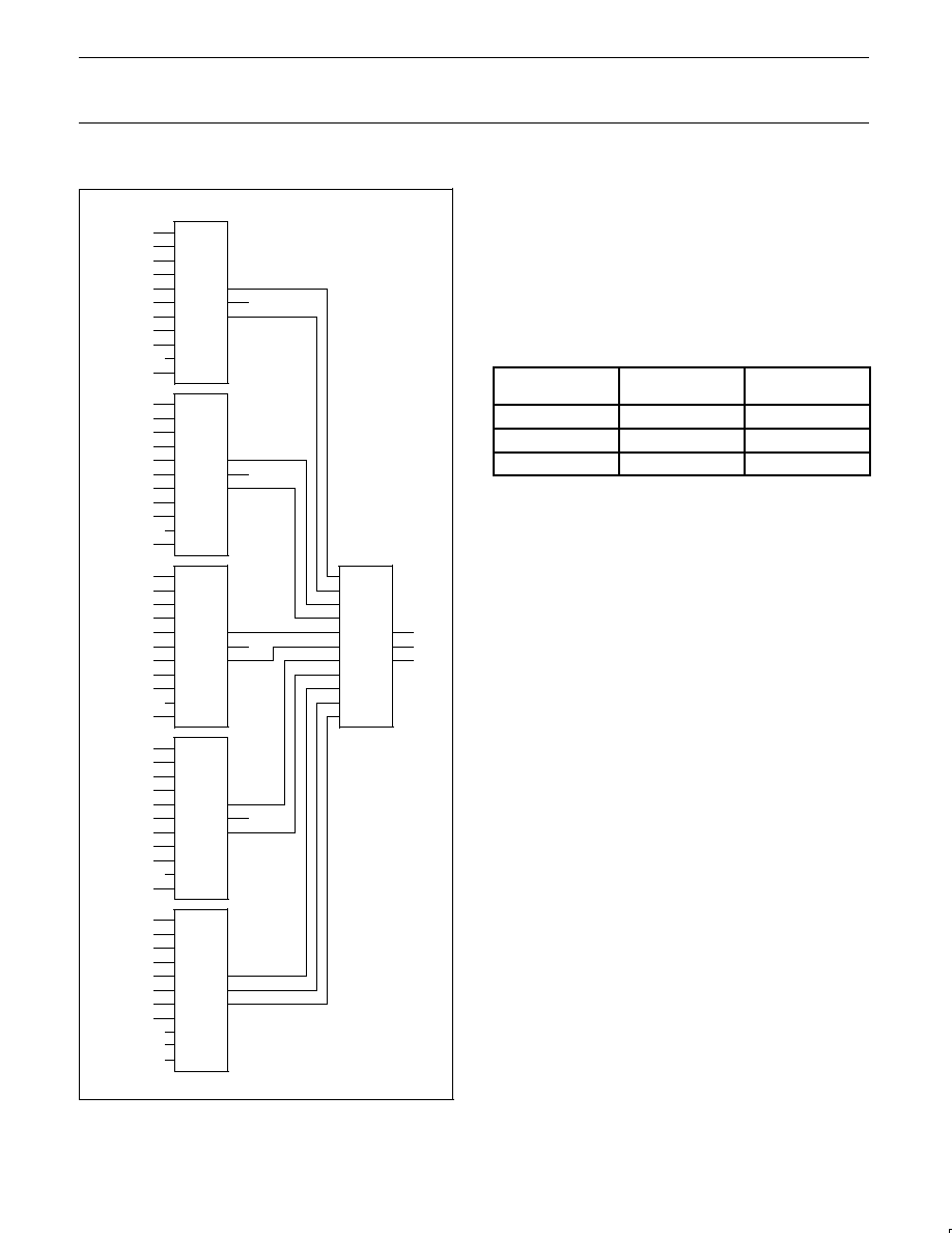
APPLICATION
B23
A23
B22
A22
B21
A21
B20
A20
B19
L
A19
INPUTS
(LSB)
B3
A3
B2
A2
B1
A1
B0
A0
IA<B
IA=B
IA>B
A<B
A=B
A>B
NC
B18
A18
B17
A17
B16
A16
B15
A15
B14
L
A14
B3
A3
B2
A2
B1
A1
B0
A0
IA<B
IA=B
IA>B
A<B
A=B
A>B
NC
B13
A13
B12
A12
B11
A11
B10
A10
B9
L
A9
B3
A3
B2
A2
B1
A1
B0
A0
IA<B
IA=B
IA>B
A<B
A=B
A>B
NC
B8
A8
B7
A7
B6
A6
B5
A5
B4
L
A4
B3
A3
B2
A2
B1
A1
B0
A0
IA<B
IA=B
IA>B
A<B
A=B
A>B
NC
B3
A3
B2
A2
B1
A1
B0
A0
H
(LSB)
B3
A3
B2
A2
B1
A1
B0
A0
IA<B
IA=B
IA>B
A<B
A=B
A>B
B3
A3
B2
A2
B1
A1
B0
A0
A<B
A=B
A>B
A<B
A=B
A>B
OUTPUTS
L
L
SF00079
Figure 1. Comparison of Two 24-Bit Words
The parallel expansion scheme shown in Figure 1 demonstrates the
most efficient general use of these comparators. The expansion
inputs can be used as a fifth input bit position except on the least
significant device, which must be connected as in the serial scheme.
The expansion inputs used by labeling I
A>B
as an "A" input, I
A<B
as
a "B" input and setting I
A=B
= Low. The 74F85 can be used as a 5-bit
comparator only when the outputs are used to drive the (A0≠A3) and
(B0≠B3) inputs of another 74F85 device. The parallel technique can
be expanded to any number of bits as shown in Table 1.
Table 1.
WORD LENGTH
NUMBER OF
PACKAGES
TYPICAL SPEEDS
74F
1≠4 bits
1
12ns
5≠24 bits
2≠6
22ns
25≠120 bits
8≠31
34ns
Philips Semiconductors
Product specification
74F85
4-bit magnitude comparator
September 27, 1994
5
ABSOLUTE MAXIMUM RATINGS
(Operation beyond the limits set forth in this table may impair the useful life of the device.
Unless otherwise noted these limits are over the operating free-air temperature range.)
SYMBOL
PARAMETER
RATING
UNIT
V
CC
Supply voltage
≠0.5 to +7.0
V
V
IN
Input voltage
≠0.5 to +7.0
V
I
IN
Input current
≠30 to +5
mA
V
OUT
Voltage applied to output in High output state
≠0.5 to V
CC
V
I
OUT
Current applied to output in Low output state
40
mA
T
amb
Operating free-air temperature range
0 to +70
∞
C
T
stg
Storage temperature range
≠65 to +150
∞
C
RECOMMENDED OPERATING CONDITIONS
SYMBOL
PARAMETER
LIMITS
UNIT
SYMBOL
PARAMETER
MIN
NOM
MAX
UNIT
V
CC
Supply voltage
4.5
5.0
5.5
V
V
IH
High-level input voltage
2.0
V
V
IL
Low-level input voltage
0.8
V
I
IK
Input clamp current
≠18
mA
I
OH
High-level output current
≠1
mA
I
OL
Low-level output current
20
mA
T
amb
Operating free-air temperature range
0
+70
∞
C
DC ELECTRICAL CHARACTERISTICS
(Over recommended operating free-air temperature range unless otherwise noted.)
SYMBOL
PARAMETER
TEST CONDITIONS
1
LIMITS
UNIT
SYMBOL
PARAMETER
TEST CONDITIONS
1
MIN
TYP
2
MAX
UNIT
V
O
High level output voltage
V
CC
= MIN, V
IL
= MAX
±
10%V
CC
2.5
V
V
OH
High-level output voltage
V
IH
= MIN, I
OH
= MAX
±
5%V
CC
2.7
3.4
V
V
O
Low level output voltage
V
CC
= MIN, V
IL
= MAX
±
10%V
CC
0.30
0.50
V
V
OL
Low-level output voltage
V
IH
= MIN, I
OL
= MAX
±
5%V
CC
0.30
0.50
V
V
IK
Input clamp voltage
V
CC
= MIN, I
I
= I
IK
≠0.73
≠1.2
V
I
I
Input current at maximum input voltage
V
CC
= 0.0V, V
I
= 7.0V
100
µ
A
I
IH
High-level input current
V
CC
= MAX, V
I
= 2.7V
20
µ
A
I
IL
Low-level input current
V
CC
= MAX, V
I
= 0.5V
≠20
µ
A
I
OS
Short-circuit output current
3
V
CC
= MAX
≠60
≠150
mA
I
CCH
V
IN
= GND
36
50
I
CC
Supply current (total)
I
CCL
V
CC
= MAX
An = Bn = I
A=B
= GND,
I
A>B
= I
A<B
= 4.5V
40
54
mA
NOTES:
1. For conditions shown as MIN or MAX, use the appropriate value specified under recommended operating conditions for the applicable type.
2. All typical values are at V
CC
= 5V, T
amb
= 25
∞
C.
3. Not more than one output should be shorted at a time. For testing I
OS
, the use of high-speed test apparatus and/or sample-and-hold
techniques are preferable in order to minimize internal heating and more accurately reflect operational values. Otherwise, prolonged shorting
of a High output may raise the chip temperature well above normal and thereby cause invalid readings in other parameter tests. In any
sequence of parameter tests, I
OS
tests should be performed last.