 | –≠–ª–µ–∫—Ç—Ä–æ–Ω–Ω—ã–π –∫–æ–º–ø–æ–Ω–µ–Ω—Ç: N74F863D | –°–∫–∞—á–∞—Ç—å:  PDF PDF  ZIP ZIP |

Philips
Semiconductors
74F862, 74F863
Bus transceivers (3-State)
Product specification
Supersedes data of 1999 Jan 08
IC15 Data Handbook
2000 Mar 24
INTEGRATED CIRCUITS
Philips Semiconductors
Product specification
74F862, 74F863
Bus transceivers (3-State)
2
2000 Mar 24
853-0881 23378
FEATURES
∑
Provide high performance bus interface buffering for wide
data/address paths or buses carrying parity
∑
High impedance NPN base inputs for reduced loading (20
µ
A in
High and Low states)
∑
I
IL
is 20
µ
A vs. 1000
µ
A for AM29861 series
∑
Buffered control inputs for light loading, or increased fan-in as
required with MOS microprocessors
∑
Positive and negative over-shoots are clamped to ground
∑
3-State outputs glitch free during power-up and power-down
∑
Slim dual In-line (DIP) 300mil package
∑
Broadside pinout compatible with AMD AM29862≠29863
∑
Outputs sink 64mA
DESCRIPTION
The 74F862 and 74F863 bus transceivers provide high performance
bus interface buffering for wide data/address paths of buses carrying
parity. The 74F863 9-bit bus transceiver has NOR-ed transmit and
receive output enables for maximum control flexibility.
TYPE
TYPICAL
PROPAGATION
DELAY
TYPICAL SUPPLY
CURRENT
(TOTAL)
74F862
6.0ns
150mA
74F863
6.0ns
115mA
ORDERING INFORMATION
PACKAGES
COMMERCIAL RANGE
V
CC
= 5V
±
10%;
T
a
= 0
∞
C to +70
∞
C
PKG DWG #
24-pin Plastic Slim
Dual In-line (300mil)
Package
N74F862N, N74F863N
SOT222-1
24-pin Plastic Small
Outline Large
1
N74F862D, N74F863D
SOT137-1
NOTE:
1. Thermal mounting techniques are recommended. See SMD
Process Applications for a discussion of thermal considerations for
surface mounted devices.
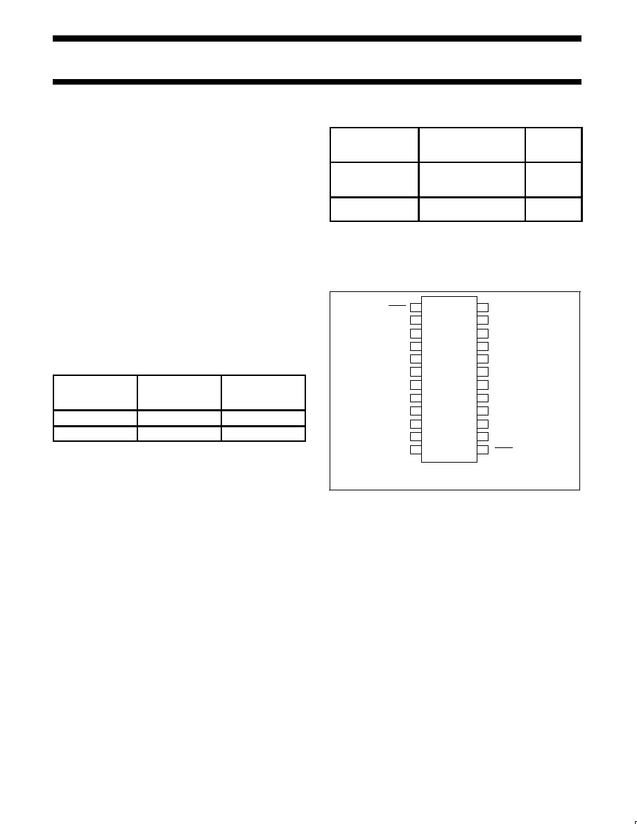
PIN CONFIGURATION
1
2
3
4
5
6
7
8
9
10
11
12
18
24
OEAB
B
0
B
1
B
2
B
3
B
4
B
5
B
6
B
7
B
8
B
9
V
CC
13
23
22
21
20
19
17
16
15
14
TOP VIEW
OEBA
A
0
A
1
A
2
A
3
A
4
A
5
A
6
A
7
A
8
A
9
GND
SF00518
Philips Semiconductors
Product specification
74F862, 74F863
Bus transceivers (3-State)
2000 Mar 24
3
PIN CONFIGURATION
1
2
3
4
5
6
7
8
9
10
11
12
18
24
OEAB
B0
B1
B2
B3
B4
B5
B6
B7
B8
B9
V
CC
13
23
22
21
20
19
17
16
15
14
TOP VIEW
74F862
OEBA
A0
A1
A2
A3
A4
A5
A6
A7
A8
A9
GND
SF00521
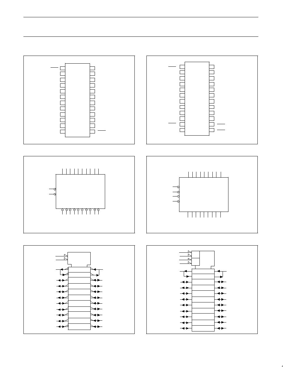
LOGIC SYMBOL
A0
1
13
OEAB
OEBA
2 3 4
5 6 7
8 9 10 11
23 22 21 20 19 18 17 16 15 14
A1 A2 A3 A4 A5 A6 A7 A8 A9
B0 B1 B2 B3 B4 B5 B6 B7 B8 B9
V
CC
= Pin 24
GND = Pin 12
74F862
SF00522
LOGIC SYMBOL (IEEE/IEC)
1
13
74F862
EN1(BA)
EN2(AB)
2
3
4
5
6
7
8
9
10
11
23
22
21
20
19
18
17
16
15
14
1
2
SF00523
PIN CONFIGURATION
1
2
3
4
5
6
7
8
9
10
11
12
18
24
OEAB1
B0
B1
B2
B3
B4
B5
B6
B7
B8
V
CC
13
23
22
21
20
19
17
16
15
14
TOP VIEW
OEBA0
A0
A1
A2
A3
A4
A5
A6
A7
A8
GND
OEBA1
OEAB0
SF01441
74F863
LOGIC SYMBOL
A0
11
1
OEBA0
OEBA1
2 3 4
5 6 7
8 9 10
23 22 21 20 19 18 17 16 15
A1 A2 A3 A4 A5 A6 A7 A8
B0 B1 B2 B3 B4 B5 B6 B7 B8
V
CC
= Pin 24
GND = Pin 12
74F863
13
14
OEAB0
OEAB1
SF00525
LOGIC SYMBOL (IEEE/IEC)
1
11
74F863
EN1(BA)
EN2(AB)
2
3
4
5
6
7
8
9
10
11
23
22
21
20
19
18
17
16
15
14
1
2
14
13
&
&
SF00526
Philips Semiconductors
Product specification
74F862, 74F863
Bus transceivers (3-State)
2000 Mar 24
4
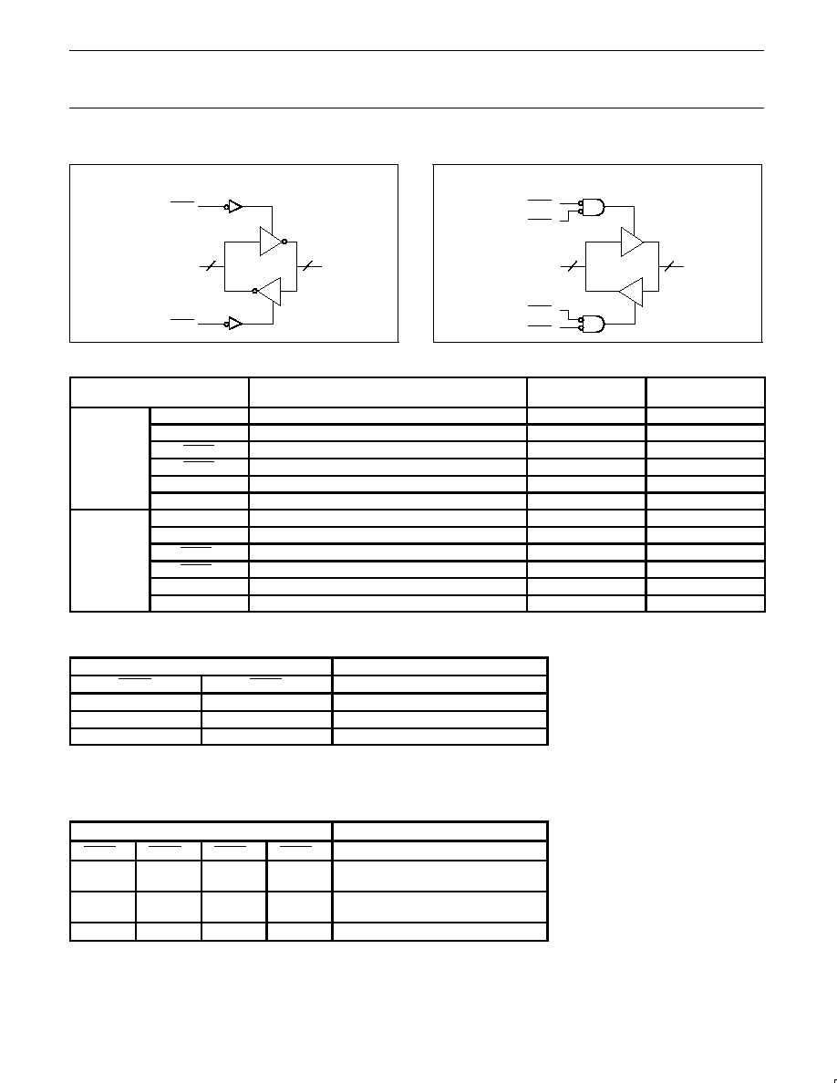
LOGIC DIAGRAM
74F862
10
10
OEAB
OEBA
An
Bn
SF00531
LOGIC DIAGRAM
74F863
9
9
OEAB0
An
Bn
OEAB1
OEBA0
OEBA1
SF00532
INPUT AND OUTPUT LOADING AND FAN-OUT TABLE
PINS
DESCRIPTION
74F(U.L.)
HIGH/LOW
LOAD VALUE
HIGH/LOW
A
0
≠ A
9
Data transmit inputs
3.5/0.117
70
µ
A/70
µ
A
B
0
≠ B
9
Data receive inputs
3.5/0.117
70
µ
A/70
µ
A
74F862
OEBA
Transmit output enable input
1.0/0.033
20
µ
A/20
µ
A
74F862
OEAB
Receive output enable input
1.0/0.033
20
µ
A/20
µ
A
A
0
≠ A
9
Data transmit outputs
1200/106.7
24mA/64mA
B
0
≠ B
9
Data receive outputs
1200/106.7
24mA/64mA
A
0
≠ A
9
Data transmit inputs
3.5/0.117
70
µ
A/70
µ
A
B
0
≠ B
9
Data receive inputs
3.5/0.117
70
µ
A/70
µ
A
74F863
OEBA
n
Transmit output enable input
1.0/0.033
20
µ
A/20
µ
A
74F863
OEAB
n
Receive output enable input
1.0/0.033
20
µ
A/20
µ
A
A
0
≠ A
9
Data transmit outputs
1200/106.7
24mA/64mA
B
0
≠ B
9
Data receive outputs
1200/106.7
24mA/64mA
NOTE: One (1.0) FAST Unit Load is defined as: 20
µ
A in the High state and 0.6mA in the Low state.
FUNCTION TABLE FOR 74F862
INPUTS
OPERATING MODES
OEAB
OEBA
74F862
L
H
A data to B bus
H
L
B bus to A data
H
H
Z
H = High voltage level
L
= Low voltage level
Z
= High impedance "off" state
FUNCTION TABLE FOR 74F863
INPUTS
OPERATING MODES
OEAB
0
OEAB
1
OEBA
0
OEBA
1
74F863
L
L0
L
L
H
X
X
H
A data to B bus
H
X
X
H
L
L
L
L
B bus to A data
H
H
H
H
Z
H = High voltage level
L
= Low voltage level
Z
= High impedance "off" state
Philips Semiconductors
Product specification
74F862, 74F863
Bus transceivers (3-State)
2000 Mar 24
5
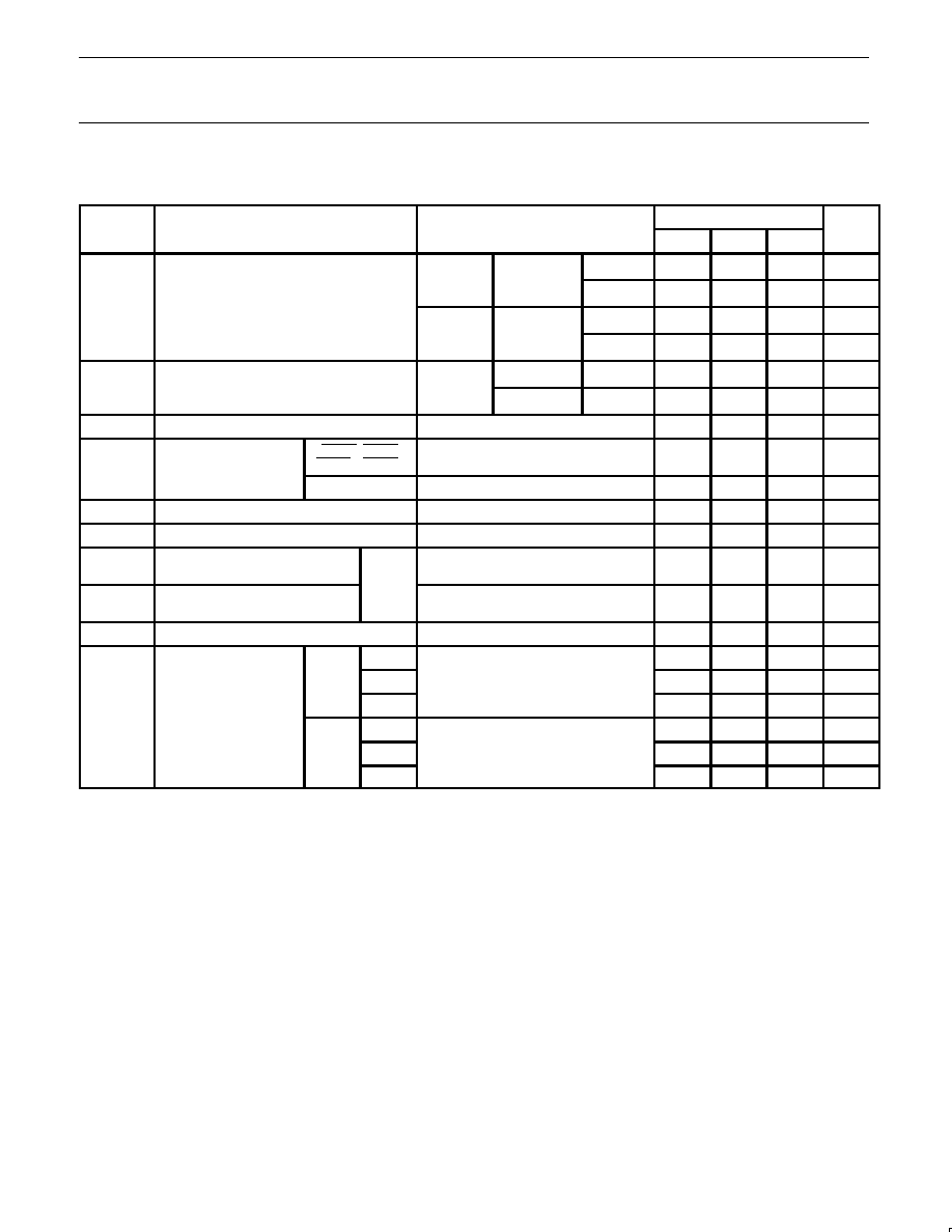
ABSOLUTE MAXIMUM RATINGS
Operation beyond the limits set forth in this table may impair the useful life of the device.
Unless otherwise noted, these limits are over the operating free-air temperature range.
SYMBOL
PARAMETER
RATING
UNIT
V
CC
Supply voltage
≠0.5 to +7.0
V
V
IN
Input voltage
≠0.5 to +7.0
V
I
IN
Input current
≠30 to +5
mA
V
OUT
Voltage applied to output in High output state
≠0.5 to +5.5
V
I
OUT
Current applied to output in Low output state
128
mA
T
a
Operating free-air temperature range
0 to +70
∞
C
T
stg
Storage temperature
≠65 to +150
∞
C
RECOMMENDED OPERATING CONDITIONS
SYMBOL
PARAMETER
LIMITS
UNIT
MIN
NOM
MAX
V
CC
Supply voltage
4.5
5.0
5.5
V
V
IH
High-level input voltage
2.0
V
V
IL
Low-level input voltage
0.8
V
I
IK
Input clamp current
≠18
mA
I
OH
High-level output current
≠24
mA
I
OL
Low-level output current
64
mA
T
a
Operating free-air temperature range
0
70
∞
C
Philips Semiconductors
Product specification
74F862, 74F863
Bus transceivers (3-State)
2000 Mar 24
6
DC ELECTRICAL CHARACTERISTICS
(Over recommended operating free-air temperature range unless otherwise noted.)
SYMBOL
PARAMETER
TEST CONDITIONS
1
LIMITS
UNIT
SYMBOL
PARAMETER
TEST CONDITIONS
1
MIN
TYP
2
MAX
UNIT
V
CC
= MIN,
V
IL
= MAX
I
O
= 1 mA
±
10%V
CC
2.4
V
V
O
High level output voltage
V
IL
= MAX,
V
IH
= MIN
I
OH
= ≠1 mA
±
5%V
CC
2.4
3.3
V
V
OH
High-level output voltage
V
CC
= MIN,
V
IL
= MAX
I
O
= 24 mA
±
10%V
CC
2.0
V
V
IL
= MAX,
V
IH
= MIN
I
OH
= ≠24 mA
±
5%V
CC
2.0
V
V
O
Low level output voltage
V
CC
= MIN,
V
IL
= MAX
I
OL
= ≠48 mA
±
10%V
CC
0.38
0.55
V
V
OL
Low-level output voltage
V
IL
= MAX,
V
IH
= MIN
I
OL
= 64 mA
±
5%V
CC
0.42
0.55
V
V
IK
Input clamp voltage
V
CC
= MIN, I
I
= I
IK
≠0.73
≠1.2
V
I
I
Input current at
maximum input voltage
OEAB, OEBA
OEAB
n
, OEBA
n
V
CC
= 0.0 V, V
I
= 7.0 V
100
µ
A
I
maximum input voltage
A
n
, B
n
V
CC
= 5.5 V, V
I
= 5.5 V
1
mA
I
IH
High-level input current
V
CC
= MAX, V
I
= 2.7 V
20
µ
A
I
IL
Low-level input current
V
CC
= MAX, V
I
= 0.5 V
≠20
µ
A
I
IH
+ I
OZH
Off-state output current
High-level voltage applied
A
B
V
CC
= MAX, V
O
= 2.7 V
70
µ
A
I
IL
+ I
OZL
Off-state output current
Low-level voltage applied
A
n
, B
n
V
CC
= MAX, V
O
= 0.5 V
≠70
µ
A
I
OS
Short-circuit output current
3
V
CC
= MAX
≠100
≠225
mA
I
CCH
145
195
mA
A
n
, B
n
74F863
I
CCL
V
CC
= MAX
140
195
mA
I
CCZ
165
220
mA
I
CC
Supply current total
I
CCH
90
130
mA
74F862
I
CCL
V
CC
= MAX
120
170
mA
I
CCZ
130
160
mA
NOTES:
1. For conditions shown as MIN or MAX, use the appropriate value specified under recommended operating conditions for the applicable type.
2. All typical values are at V
CC
= 5 V, T
a
= 25
∞
C.
3. Not more than one output should be shorted at a time. For testing I
OS
, the use of high-speed test apparatus and/or sample-and-hold
techniques are preferable in order to minimize internal heating and more accurately reflect operational values. Otherwise, prolonged shorting
of a High output may raise the chip temperature well above normal and thereby cause invalid readings in other parameter tests. In any
sequence of parameter tests, I
OS
tests should be performed last.
Philips Semiconductors
Product specification
74F862, 74F863
Bus transceivers (3-State)
2000 Mar 24
7
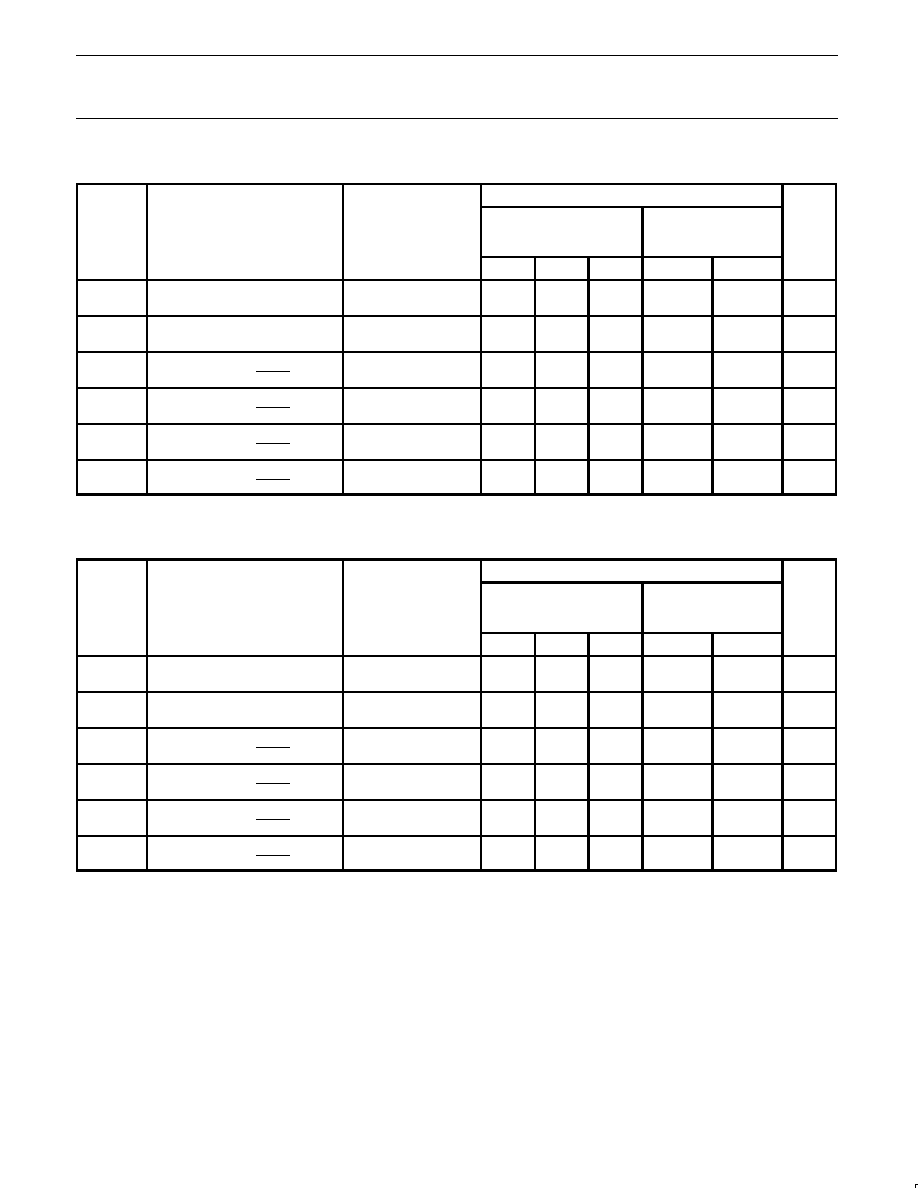
AC ELECTRICAL CHARACTERISTICS
74F863
SYMBOL
PARAMETER
TEST CONDITION
T
a
= +25
∞
C
V
CC
= 5 V
C
L
= 50 pF, R
L
= 500
T
a
= 0
∞
C to +70
∞
C
V
CC
= 5 V
±
10%
C
L
= 50 pF, R
L
= 500
UNIT
MIN
TYP
MAX
MIN
MAX
t
PLH
t
PHL
Propagation delay
A
n
or B
n
Waveform 1
4.0
3.0
6.0
5.0
9.0
8.0
3.5
2.5
10.0
9.0
ns
t
PLH
t
PHL
Propagation delay
B
n
or A
n
Waveform 1
4.0
2.5
6.0
5.0
9.0
8.0
3.5
2.5
10.0
9.0
ns
t
PZH
t
PZL
Output Enable time
High or Low level OEBA
n
to A
n
Waveform 3
Waveform 4
6.0
4.0
8.0
6.0
11.5
10.0
5.0
4.0
13.0
11.0
ns
t
PZH
t
PZL
Output Enable time
High or Low level OEAB
n
to B
n
Waveform 3
Waveform 4
6.0
4.0
8.0
6.0
11.0
10.0
5.0
4.0
13.0
11.0
ns
t
PHZ
t
PLZ
Output Disable time
High or Low level OEBA
n
to A
n
Waveform 3
Waveform 4
3.5
2.5
5.5
5.0
9.0
8.5
3.0
2.0
9.5
9.5
ns
t
PHZ
t
PLZ
Output Disable time
High or Low level OEAB
n
to B
n
Waveform 3
Waveform 4
3.5
2.5
5.5
4.5
8.5
8.5
3.0
2.0
9.5
9.5
ns
AC ELECTRICAL CHARACTERISTICS
74F862
SYMBOL
PARAMETER
TEST CONDITION
T
a
= +25
∞
C
V
CC
= 5 V
C
L
= 50 pF, R
L
= 500
T
a
= 0
∞
C to +70
∞
C
V
CC
= 5 V
±
10%
C
L
= 50 pF, R
L
= 500
UNIT
MIN
TYP
MAX
MIN
MAX
t
PLH
t
PHL
Propagation delay
A
n
or B
n
Waveform 2
4.0
1.5
6.0
3.5
9.0
6.5
3.0
1.5
10.0
7.0
ns
t
PLH
t
PHL
Propagation delay
B
n
or A
n
Waveform 2
4.0
1.5
6.0
3.5
9.0
6.5
3.5
1.5
10.0
7.0
ns
t
PZH
t
PZL
Output Enable time
High or Low level OEBA
n
to A
n
Waveform 3
Waveform 4
6.5
6.0
8.5
7.5
12.0
12.0
5.5
5.0
13.5
14.0
ns
t
PZH
t
PZL
Output Enable time
High or Low level OEAB
n
to B
n
Waveform 3
Waveform 4
6.5
6.0
8.5
7.5
12.0
12.0
5.5
5.0
13.5
14.0
ns
t
PHZ
t
PLZ
Output Disable time
High or Low level OEBA
n
to A
n
Waveform 3
Waveform 4
3.0
2.5
5.0
4.0
8.5
8.5
2.5
2.0
9.5
9.0
ns
t
PHZ
t
PLZ
Output Disable time
High or Low level OEAB
n
to B
n
Waveform 3
Waveform 4
3.0
2.5
5.0
4.0
8.5
8.5
2.5
2.0
9.5
9.0
ns
Philips Semiconductors
Product specification
74F862, 74F863
Bus transceivers (3-State)
2000 Mar 24
8
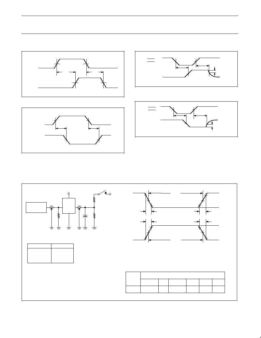
AC WAVEFORMS
V
M
V
M
V
M
V
M
Bn, An
An, Bn
t
PLH
t
PHL
SF00202
Waveform 1. Propagation Delay for Non-inverting Output
A
n
or B
n
B
n
or A
n
t
PLH
V
M
V
M
V
M
V
M
t
PHL
SF00534
Waveform 2. Propagation Delay for Inverting Output
A
n
, B
n
OEBA
n
OEAB
n
t
PZH
V
M
V
M
V
M
t
PHZ
V
OH
≠0.3 V
SF00535
0 V
Waveform 3. 3-State Output Enable Time to High Level and
Output Disable Time from High Level
A
n
, B
n
OEBA
n
OEAB
n
t
PZL
V
M
V
M
V
M
t
PLZ
V
OL
+0.3 V
SF00536
Waveform 4. 3-State Output Enable Time to Low Level and
Output Disable Time from Low Level
NOTE: For all waveforms, VM = 1.5V.
TEST CIRCUITS AND WAVEFORMS
tw
90%
VM
10%
90%
VM
10%
90%
VM
10%
90%
VM
10%
NEGATIVE
PULSE
POSITIVE
PULSE
tw
AMP (V)
0V
0V
tTHL (tf
)
INPUT PULSE REQUIREMENTS
rep. rate
t
w
t
TLH
t
THL
1MHz
500ns
2.5ns
2.5ns
Input Pulse Definition
VCC
family
74F
D.U.T.
PULSE
GENERATOR
RL
CL
RT
VIN
VOUT
Test Circuit for Open Collector Outputs
DEFINITIONS:
R
L
= Load resistor;
see AC electrical characteristics for value.
C
L
= Load capacitance includes jig and probe capacitance;
see AC electrical characteristics for value.
R
T
= Termination resistance should be equal to Z
OUT
of
pulse generators.
tTHL (tf
)
tTLH (tr
)
tTLH (tr
)
AMP (V)
amplitude
3.0V
1.5V
V
M
RL
7.0V
SF00128
TEST
SWITCH
t
PLZ
closed
t
PZL
closed
All other
open
SWITCH POSITION
Philips Semiconductors
Product specification
74F862, 74F863
Bus transceivers (3-State)
2000 Mar 24
9
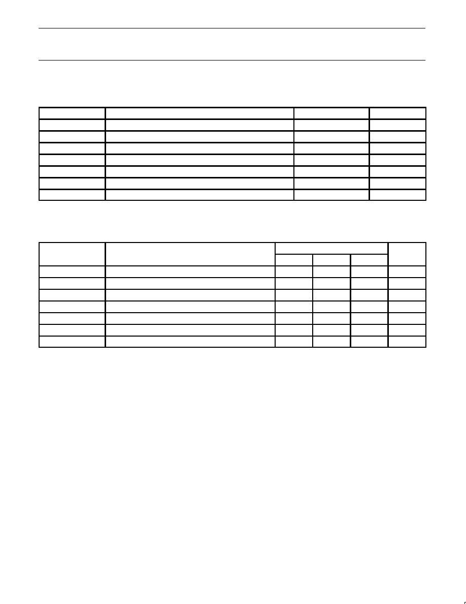
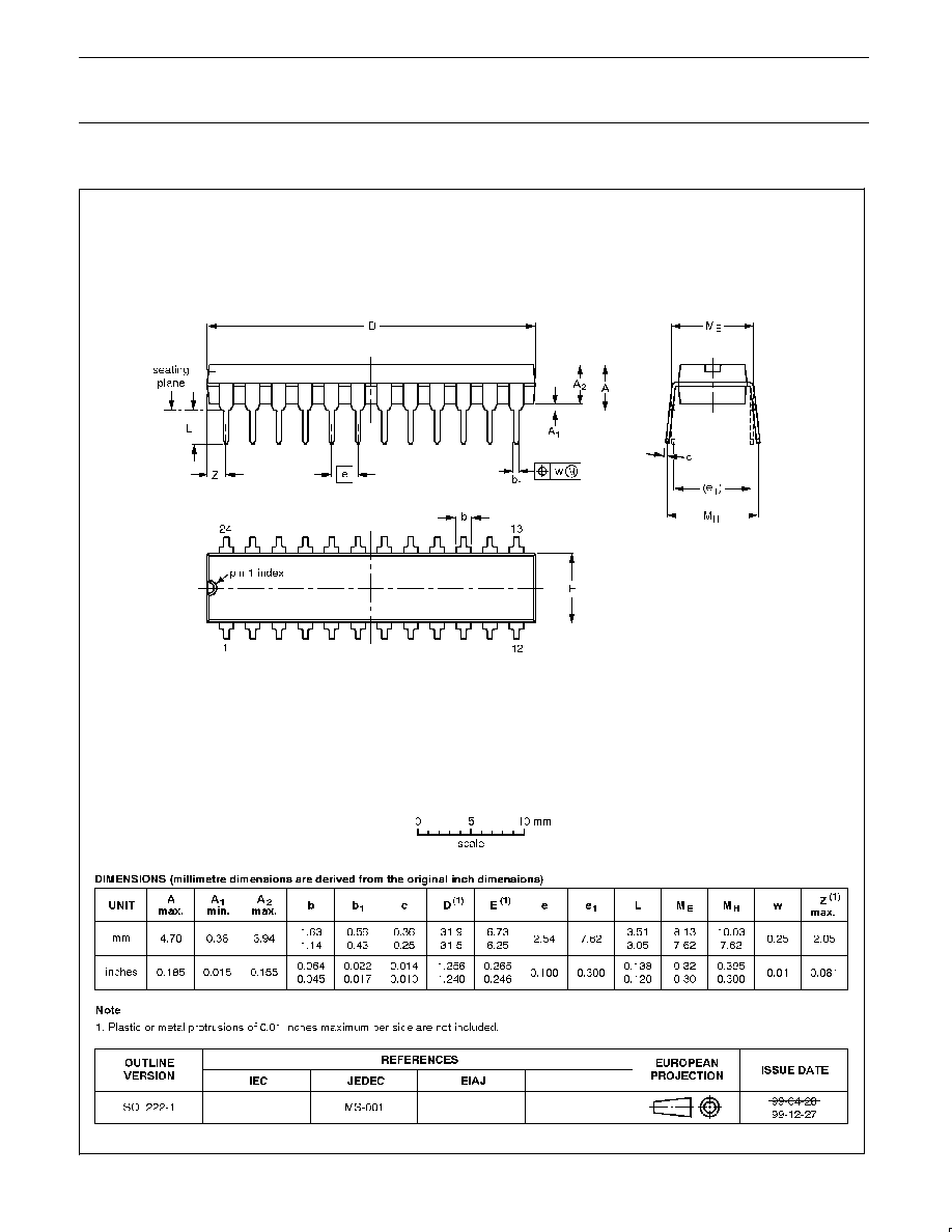
DIP24:
plastic dual in-line package; 24 leads (300 mil)
SOT222-1
Philips Semiconductors
Product specification
74F862, 74F863
Bus transceivers (3-State)
2000 Mar 24
10
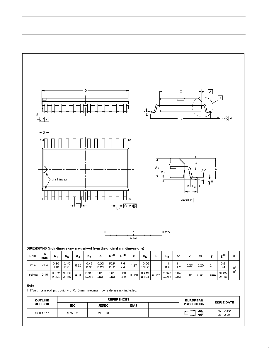
SO24:
plastic small outline package; 24 leads; body width 7.5 mm
SOT137-1

Philips Semiconductors
Product specification
74F862, 74F863
Bus transceivers (3-State)
2000 Mar 24
11
NOTES

Philips Semiconductors
Product specification
74F862, 74F863
Bus transceivers (3-State)
2000 Mar 24
12
Definitions
Short-form specification -- The data in a short-form specification is extracted from a full data sheet with the same type number and title. For
detailed information see the relevant data sheet or data handbook.
Limiting values definition -- Limiting values given are in accordance with the Absolute Maximum Rating System (IEC 134). Stress above one
or more of the limiting values may cause permanent damage to the device. These are stress ratings only and operation of the device at these or
at any other conditions above those given in the Characteristics sections of the specification is not implied. Exposure to limiting values for extended
periods may affect device reliability.
Application information -- Applications that are described herein for any of these products are for illustrative purposes only. Philips
Semiconductors make no representation or warranty that such applications will be suitable for the specified use without further testing or
modification.
Disclaimers
Life support -- These products are not designed for use in life support appliances, devices or systems where malfunction of these products can
reasonably be expected to result in personal injury. Philips Semiconductors customers using or selling these products for use in such applications
do so at their own risk and agree to fully indemnify Philips Semiconductors for any damages resulting from such application.
Right to make changes -- Philips Semiconductors reserves the right to make changes, without notice, in the products, including circuits, standard
cells, and/or software, described or contained herein in order to improve design and/or performance. Philips Semiconductors assumes no
responsibility or liability for the use of any of these products, conveys no license or title under any patent, copyright, or mask work right to these
products, and makes no representations or warranties that these products are free from patent, copyright, or mask work right infringement, unless
otherwise specified.
Philips Semiconductors
811 East Arques Avenue
P.O. Box 3409
Sunnyvale, California 94088≠3409
Telephone 800-234-7381
©
Copyright Philips Electronics North America Corporation 2000
All rights reserved. Printed in U.S.A.
Date of release: 03-00
Document order number:
9397 750 06999
Philips
Semiconductors
Data sheet
status
Objective
specification
Preliminary
specification
Product
specification
Product
status
Development
Qualification
Production
Definition
[1]
This data sheet contains the design target or goal specifications for product development.
Specification may change in any manner without notice.
This data sheet contains preliminary data, and supplementary data will be published at a later date.
Philips Semiconductors reserves the right to make changes at any time without notice in order to
improve design and supply the best possible product.
This data sheet contains final specifications. Philips Semiconductors reserves the right to make
changes at any time without notice in order to improve design and supply the best possible product.
Data sheet status
[1]
Please consult the most recently issued datasheet before initiating or completing a design.