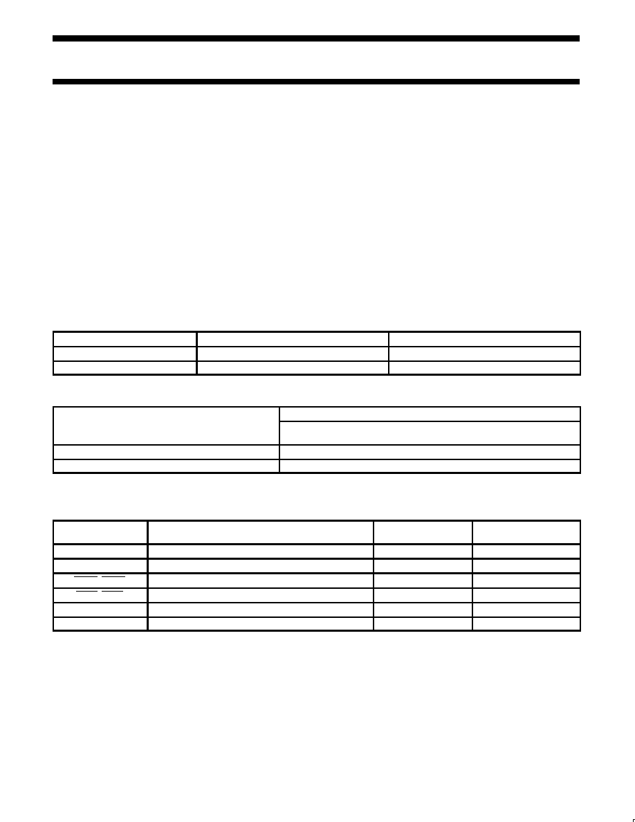
 | –≠–ª–µ–∫—Ç—Ä–æ–Ω–Ω—ã–π –∫–æ–º–ø–æ–Ω–µ–Ω—Ç: N74F8963Y | –°–∫–∞—á–∞—Ç—å:  PDF PDF  ZIP ZIP |
Document Outline
- FEATURES
- DESCRIPTION
- ORDERING INFORMATION
- INPUT AND OUTPUT LOADING AND FAN OUT TABLE
- PIN CONFIGURATION FLATPACK AND PLCC
- IEC/IEEE SYMBOL
- PIN DESCRIPTION
- LOGIC SYMBOL FOR 74F8962
- LOGIC SYMBOL FOR 74F8963
- LOGIC DIAGRAM
- FUNCTION TABLE FOR 74F8962
- FUNCTION TABLE FOR 74F8963
- ABSOLUTE MAXIMUM RATINGS
- RECOMMENDED OPERATING CONDITIONS
- DC ELECTRICAL CHARACTERISTICS
- AC ELECTRICAL CHARACTERISTICS FOR 74F8962
- AC SETUP REQUIREMENTS FOR 74F8962
- AC ELECTRICAL CHARACTERISTICS FOR 74F8963
- AC SETUP REQUIREMENTS FOR 74F8963
- AC WAVEFORMS
- TEST CIRCUITS AND WAVEFORMS
Philips Semiconductors FAST Products
Product specification
74F8962/8963
9-Bit latched bidirectional Futurebus transceivers
(open-collector)
1
March 11, 1993
853≠1425 09230
FEATURES
∑
Octal latched transceiver
∑
Drives heavily loaded backplanes with
equivalent load impedances down to 10
∑
High drive (100mA) open collector drivers
on B port
∑
Reduced voltage swing (1 volt) produces
less noise and reduces power consumption
∑
High speed operation enhances
performance of backplane buses and
facilitates incident wave switching
∑
Compatible with IEEE 896 futurebus
standards
∑
Built≠in precision band≠gap reference
provides accurate receiver thresholds and
improved noise immunity
∑
Multiple GND pins minimize ground bounce
∑
Glitch≠free power up/power down
operation
DESCRIPTION
The 74F8962 and 74F8963 are octal
bidirectional latched transceivers and are
intended to provide the electrical interface to
a high performance wired-OR bus. The B port
inverting drivers are low-capacitance open
collector with controlled ramp and are
designed to sink 100mA from 2 volts. The B
port inverting receivers have a 150mV
threshold region.
The B port interfaces to `Backplane
Transceiver Logic' (BTL). BTL features a
reduced (1V to 2V) voltage swing for lower
power consumption and a series diode on
the drivers to reduce capacitive loading.
Incident wave switching to 9
is guaranteed.
The voltage swing is much less for BTL, so is
its receiver threshold region, therefore noise
margins are excellent.
BTL offers low power consumption, low
ground bounce, EMI and crosstalk, low
capacitive loading, superior noise margin and
low propagation delays. This results in a high
bandwidth, reliable backplane.
The 74F8962 and 74F8963 A ports have TTL
3-state drivers and TTL receivers with a latch
function.
The 74F8963 is the non-inverting version of
74F8962.
TYPE
TYPICAL PROPAGATION DELAY
TYPICAL SUPPLY CURRENT( TOTAL)
74F8962
6.5ns
90mA
74F8963
5.5ns
90mA
ORDERING INFORMATION
ORDER CODE
DESCRIPTION
COMMERCIAL RANGE
V
CC
= 5V
±
10%, T
amb
= 0
∞
C to +70
∞
C
44≠pin Quad Flat Pack
1
N74F8962Y, N74F8963Y
44≠pin Plastic Leaded Chip Carrier
N74F8962A, N74F8963A
Note to ordering information
1. Flatpack package is not available at this time.
INPUT AND OUTPUT LOADING AND FAN OUT TABLE
PINS
DESCRIPTION
74F (U.L.)
HIGH/LOW
LOAD VALUE
HIGH/LOW
AI0 ≠ AI8
PNP latched inputs
1.0/0.167
20
µ
A/100
µ
A
B0 ≠ B8
Data inputs with threshold circuitry
5.0/0.167
100
µ
A/100
µ
A
OEAB, OEBA
Output enable inputs (active low)
1.0/0.033
20
µ
A/20
µ
A
LEAB, LEBA
Latch enable inputs (active low)
1.0/0.033
20
µ
A/20
µ
A
AO0 ≠ AO8
3≠state outputs
150/40
3mA/24mA
B0 ≠ B8
Open collector outputs
OC/166.7
OC/100mA
Notes to input and output loading and fan out table
1. One (1.0) FAST unit load is defined as: 20
µ
A in the high state and 0.6mA in the low state.
2. OC = Open collector.
Philips Semiconductors FAST Products
Product specification
74F8962/8963
9-Bit latched bidirectional Futurebus transceivers
(open-collector)
March 11, 1993
2
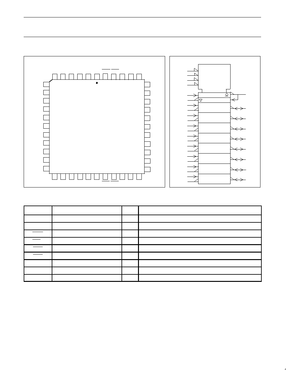
PIN CONFIGURATION FLATPACK AND PLCC
IEC/IEEE SYMBOL
74F8962
6
5
4
3
2
1
39
38
37
36
35
34
13
12
11
10
9
8
24
22
23
21
20
19
44
33
18
7
AO0
AI1
AO1
GND
AI0
VCC OEBA
AO7
AI7
GND
28
26
27
25
43
42
41
40
LEBA BO
GND
B1
32
31
30
29
17
16
15
14
AI2
AO2
A13
AO3
AI4
GND
AO4
AI5
AO5
AI6
AO6
AI8 AO8
VCC LEAB OEAB B8
GND
B7
GND
B2
GND
B3
GND
B4
GND
B5
GND
B6
GND
74F8962
42
EN1
EN2
EN3
EN4
1
24
25
43
44
40
38
36
34
32
30
28
26
2
3
4
5
7
8
9
10
11
13
14
15
16
17
19
20
21
22
2
4
3D
PIN DESCRIPTION
SYMBOL
PINS
TYPE
NAME AND FUNCTION
AI0 ≠ AI8
2, 4, 7, 9, 11, 14, 16, 19, 21
Input
PNP latched inputs.
B0 ≠ B8
42, 40, 38, 36, 34, 32, 30, 28, 26
I/O
Data input / open collector output, high current drives.
OEAB
25
Input
Output enable input. Enables the B outputs when low.
OEBA
44
Input
Output enable input. Enables the A outputs when high.
LEAB
24
Input
Latch enable input. Enables the AB latches low.
LEBA
43
Input
Latch enable input. Enables the BA latches low.
AO0 ≠ AO8
3, 5, 8, 10, 13, 15, 17, 20, 22
Output
TTL 3≠state outputs.
GND
6, 12, 18, 27, 29, 31, 33, 35, 37, 39, 41
Ground
Grounds
V
CC
1, 23
Power
Positive supply voltages

Philips Semiconductors FAST Products
Product specification
74F8962/8963
9-Bit latched bidirectional Futurebus transceivers
(open-collector)
March 11, 1993
3
LOGIC SYMBOL FOR 74F8962
OEBA
OEAB
LEAB
LEBA
AI0 AO0 AI1 AO1 AI2 AO2 AI3 AO3 AI4 AO4 AI5 AO5 AI6 AO6 AI7 AO7 AI8 AO8
42 40 38
B0 B1 B2
36 34 32
30 28 26
B6 B7 B8
B3 B4 B5
VCC = Pin 1, 23
GND = Pin 6, 12, 18, 27, 29, 31, 33, 35, 37, 39, 41
74F8962
2
3
4
5
7
8
9
10
11
13 14
15 16
17 19
20 21
22
25
24
43
44
LOGIC SYMBOL FOR 74F8963
OEBA
OEAB
LEAB
LEBA
AI0 AO0 AI1 AO1 AI2 AO2 AI3 AO3 AI4 AO4 AI5 AO5 AI6 AO6 AI7 AO7 AI8 AO8
42 40 38
B0 B1 B2
36 34 32
30 28 26
B6 B7 B8
B3 B4 B5
74F8963
25
24
43
44
VCC = Pin 1, 23
GND = Pin 6, 12, 18, 27, 29, 31, 33, 35, 37, 39, 41
2
3
4
5
7
8
9
10
11
13 14
15 16
17 19
20 21
22

Philips Semiconductors FAST Products
Product specification
74F8962/8963
9-Bit latched bidirectional Futurebus transceivers
(open-collector)
March 11, 1993
4
LOGIC DIAGRAM
B0
B1
B2
B3
B4
B5
B6
B7
B8
Data
E
Q
VCC
= Pin 1, 23
GND = Pin 6, 12, 18, 27, 29, 31, 33, 37, 39, 41
Q
Data
E
Q
Data
E
Q
Data
E
Q
Data
E
Q
Data
E
Q
Data
E
Q
Data
E
Q
Data
E
Q
Data
E
Q
Data
E
Q
Data
E
Q
Data
E
Q
Data
E
Q
Data
E
Q
Data
E
Q
Data
E
Q
42
40
38
36
34
32
30
28
26
AI0
AO0
AI1
AO1
AI2
AO2
AI3
AO3
AI4
AO4
AI5
AO5
AI6
AO6
AI7
AO7
AI8
AO8
2
3
4
5
7
8
9
10
11
13
14
15
16
17
19
20
21
22
OEAB
LEBA
LEAB
OEBA
25
43
24
44
B0
B1
B2
B3
B4
B5
B6
B7
B8
Data
E
Q
Data
E
Q
Data
E
Q
Data
E
Q
Data
E
Q
Data
E
Q
Data
E
Q
Data
E
Q
Data
E
Q
Data
E
Q
Data
E
Q
Data
E
Q
Data
E
Q
Data
E
Q
Data
E
Q
Data
E
Q
Data
E
Q
Data
E
Q
42
40
38
36
34
32
30
28
26
AI0
AO0
AI1
AO1
AI2
AO2
AI3
AO3
AI4
AO4
AI5
AO5
AI6
AO6
AI7
AO7
AI8
AO8
2
3
4
5
7
8
9
10
11
13
14
15
16
17
19
20
21
22
OEAB
LEBA
LEAB
OEBA
25
43
24
44
74F8962
74F8963
Data
E
Philips Semiconductors FAST Products
Product specification
74F8962/8963
9-Bit latched bidirectional Futurebus transceivers
(open-collector)
March 11, 1993
5
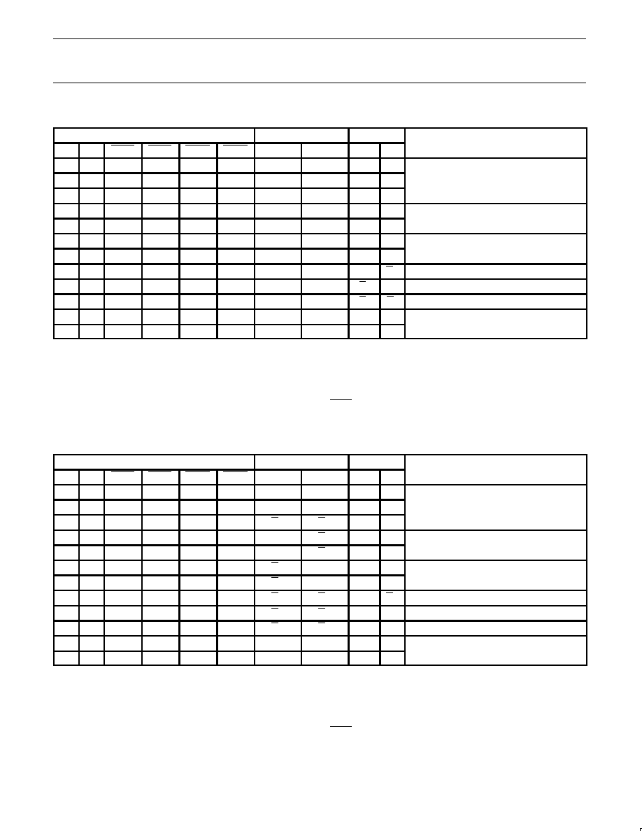
FUNCTION TABLE FOR 74F8962
INPUTS
LATCH STATES
OUTPUTS
OPERATING MODE
AIn
Bn*
LEAB
LEBA
OEAB
OEBA
AB
BA
AOn
Bn
H
H
L
L
H
H
H
H
Z
X
L
L
L
L
H
H
L
L
Z
X
B and AO disabled
X
X
H
H
H
H
Qn
Qn
Z
X
H
≠
L
X
L
H
H
Qn
Z
L
AO 3≠state, transparent data from AI to B
L
≠
L
X
L
H
L
Qn
Z
H**
X
H
X
L
H
L
Qn
H
L
X
B disabled, transparent data from B to AO
X
L
X
L
H
L
Qn
L
H
X
X
X
H
X
L
H
Qn
Qn
Z
Qn
AO 3≠state, latched data to B
X
X
X
H
H
L
Qn
Qn
Qn
X
B disabled, latched to AO
X
X
H
H
L
L
Qn
Qn
Qn
Qn
Latched state to AO and B
H
≠
L
L
L
L
H
L
H
L
Read back from AI to B to AO
L
≠
L
L
L
L
L
H
L
H**
(both latches transparent)
Notes to function table for 74F8962
1. H = High voltage level
2. L
= Low voltage level
3. X = Don't care
4. ≠
= Input not externally driven
5. Z = High impedance "off' state
6. Q
n
= High or low voltage level one setup time prior to the low≠to≠high LEXX transition.
7. H**= Goes to level of pullup voltage.
8. B* = Precaution should be taken to insure B inputs do not float. If they do they are equal to low state.
FUNCTION TABLE FOR 74F8963
INPUTS
LATCH STATES
OUTPUTS
OPERATING MODE
AIn
Bn*
LEAB
LEBA
OEAB
OEBA
AB
BA
AOn
Bn
H
H
L
L
H
H
L
L
Z
X
L
L
L
L
H
H
H
H
Z
X
B and AO disabled
X
X
H
H
H
H
Qn
Qn
Z
X
H
≠
L
X
L
H
L
Qn
Z
H
AO 3≠state, transparent data from AI to B
L
≠
L
X
L
H
H
Qn
Z
L
X
H
X
L
H
L
Qn
L
H
X
B disabled, transparent data from B to AO
X
L
X
L
H
L
Qn
H
L
X
X
X
H
X
L
H
Qn
Qn
Z
Qn
AO 3≠state, latched data to B
X
X
X
H
H
L
Qn
Qn
Qn
X
B disabled, latched to AO
X
X
H
H
L
L
Qn
Qn
Qn
Qn
Latched state to AO and B
H
≠
L
L
L
L
L
L
H
H**
Read back from AI to B to AO
L
≠
L
L
L
L
H
L
L
L
(both latches transparent)
Notes to function table for 74F8963
1. H = High voltage level
2. L
= Low voltage level
3. X = Don't care
4. ≠
= Input not externally driven
5. Z = High impedance "off" state
6. Q
n
= High or low voltage level one setup time prior to the low≠to≠high LEXX transition.
7. H**= Goes to level of pullup voltage.
8. B* = Precaution should be taken to insure B inputs do not float. If they do they are equal to low state.