Philips Semiconductors FAST Products
Product specification
74F8965/74F8966
9-Bit address/data Futurebus transceiver, ADT
1
December 19, 1990
853 1526 01320
FEATURES
∑
9≠bit transceiver (both directions)
∑
Drives heavily loaded backplanes with
equivalent load impedances down to
10 ohms
∑
High drive (100mA) open collector
drivers on B port
∑
Reduced voltage swing (1V to 2V)
produces less noise and reduces
power consumption
∑
High speed operation enhances
performance of backplane buses and
facilitates incident wave switching
∑
Compatible with IEEE 896 futurebus
standards and IEEE 1194 BTL stan-
dard
∑
Built≠in precision band≠gap reference
provides accurate receiver thresholds
and improved noise immunity
∑
Controlled output ramp and multiple
GND pins minimize ground bounce
∑
Glitch≠free power up/power down
operation
∑
Guaranteed skew of less than 2ns
DESCRIPTION
The 74F8965 and 74F8966 are 9≠bit
bidirectional latchable transceivers and are
intended to provide the electrical interface to
a high performance wired≠OR bus. The B
port inverting drivers are low≠capacitance
open collector with controlled ramp and are
designed to sink 100mA from 2 volts. The B
port inverting receivers have a precision band
gap references for improved noise margins.
The B port interfaces to 'Backplane
Transceiver Logic' (BTL). BTL features a
reduced (1V to 2V) voltage swing for lower
power consumption and a series diode on
the drivers to reduce capacitive loading.
Incident wave switching is employed, there-
fore BTL propagation delays are short. Al-
though the voltage swing is much less for
BTL, so is its receiver threshold region,
therefore noise margins are excellent.
BTL offers low power consumption, low
ground bounce, EMI and crosstalk, low
capacitive loading, superior noise margin and
low propagation delays. This results in a high
bandwidth, reliable backplane.
The 74F8965 and 74F8966 A ports have TTL
3≠state drivers and TTL receivers.
The B ports have standard BTL I/O with
100mA current sink capability. The B≠to≠A
path is a simple inverted buffered path. When
going from A≠to≠B the user may choose be-
tween a buffered path or a latching function.
The 74F8966 also has an idle arbitrator/multi-
ple competitors output. The IAMC output
compares, using a wired≠OR configuration,
the data on the bus to the latched data pres-
ented to the bus. If the bus data matches the
data presented by the 74F8966 then IAMC is
high. If the data doesn't match then IAMC
goes low.
TYPE
TYPICAL PROPAGATION DELAY
TYPICAL SUPPLY CURRENT( TOTAL)
74F8965
3.5ns
80mA
74F8966
3.5ns
80mA
ORDERING INFORMATION
ORDER CODE
DESCRIPTION
COMMERCIAL RANGE
V
CC
= 5V
±
10%, T
amb
= 0
∞
C to +70
∞
C
44≠pin PLCC
N74F8965A, N74F8966A
INPUT AND OUTPUT LOADING AND FAN OUT TABLE
PINS
DESCRIPTION
74F (U.L.)
HIGH/LOW
LOAD VALUE
HIGH/LOW
A0 ≠ A8
TTL data inputs
1.0/0.033
20
µ
A/20
µ
A
B0 ≠ B8
Data inputs with threshold circuitry
5.0/0.167
100
µ
A/100
µ
A
OEA, OEB0, OEB1
Output enable inputs
1.0/0.167
20
µ
A/100
µ
A
LS
Latch select (active low) ('F8965)
1.0/0.167
20
µ
A/100
µ
A
IAREQ
Idle arbitration request (active low) ('F8965)
1.0/0.167
20
µ
A/100
µ
A
LE
Latch enable input (active low)
1.0/0.167
20
µ
A/100
µ
A
A0 ≠ A8
3≠state TTL outputs
150/40
3mA/24mA
B0 ≠ B8
Open collector BTL outputs
OC/166.7
OC/100mA
IAMC
Idle arbitration/multiple competitors output ('F8966)
OC/80
OC/48mA
Notes to input and output loading and fan out table
1. One (1.0) FAST unit load is defined as: 20
µ
A in the high state and 0.6mA in the low state.
2. OC = Open collector.
Philips Semiconductors FAST Products
Product specification
74F8965/74F8966
9-Bit address/data Futurebus transceiver, ADT
December 19, 1990
3
LOGIC SYMBOL
A0 A1 A2 A3 A4 A5 A6 A7 A8
Logic VCC = Pin 3, 21
Logic GND = Pin 5, 7, 9, 11, 14, 16, 18, 20
74F8965
1
44
23
22
2
OEB0
OEB1
LS
LE
OEA
4
6
8
10 12 13 15 17 19
B0 B1 B2 B3 B4 B5 B6 B7 B8
41 39 37 35 33 31 29 27 25
A0 A1 A2 A3 A4 A5 A6 A7 A8
74F8966
1
44
23
22
2
20
OEB0
OEB1
IAREQ
LE
OEA
IAMC
4
6
8
10 12 13 15 17 19
B0 B1 B2 B3 B4 B5 B6 B7 B8
41 39 37 35 33 31 29 27 25
Logic VCC = Pin 3, 21
Logic GND = Pin 5, 7, 9, 11, 14, 16, 18
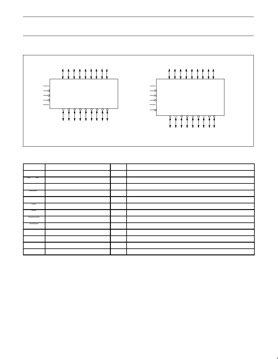
PIN DESCRIPTION
SYMBOL
PINS
TYPE
NAME AND FUNCTION
A0 ≠ A8
4, 6, 8, 10, 12, 13, 15, 17, 19
I/O
Data inputs/TTL 3≠state outputs
B0 ≠ B8
41, 39, 37, 35, 33, 31, 29, 27, 25
I/O
Data inputs / open collector outputs, high current drives.
OEB0
1
Input
Output enable input. Enables the B outputs when high.
OEB1
44
Input
Output enable input. Enables the B outputs when low.
OEA
2
Input
Output enable input. Enables the A outputs when high.
LE
22
Input
Latch enable input. Enables latch when low.
LS
23
Input
Latch select input. Selects latch when low (74F8965).
IAREQ
23
Input
Idle arbitration request input (74F8966).
IAMC
20
Output
Idle arbitration/multiple competitors output (open collector output) (74F8966).
Bus GND
26, 28, 30, 32, 34, 36, 38, 40, 42
Ground
Bus ground (0V)
Logic GND
5, 7, 9, 11, 14, 16, 18, 20 (74F8965)
Ground
Logic ground (0V)
Bus V
CC
24, 43
Power
Positive supply voltages
Logic V
CC
3, 21
Power
Positive supply voltages