 | –≠–ª–µ–∫—Ç—Ä–æ–Ω–Ω—ã–π –∫–æ–º–ø–æ–Ω–µ–Ω—Ç: NE527D | –°–∫–∞—á–∞—Ç—å:  PDF PDF  ZIP ZIP |
Philips Semiconductors Linear Products
Product specification
NE527
Voltage comparator
315
August 31, 1994
853-0906 13721
DESCRIPTION
The NE527 is a high-speed analog voltage comparator which, for
the first time, mates state-of-the-art Schottky diode technology with
the conventional linear process. This allows simultaneous
fabrication of high speed TTL gates with a precision linear amplifier
on a single monolithic chip. The NE527 is similar in design to the
Philips Semiconductors NE529 voltage comparator except that it
incorporates an "Emitter-Follower" input stage for extremely low
input currents. This opens the door to a whole new range of
applications for analog voltage comparators.
FEATURES
∑
15ns propagation delay
∑
Complementary output gates
∑
TTL or ECL compatible outputs
∑
Wide common-mode and differential voltage range
∑
Typical gain of 5000
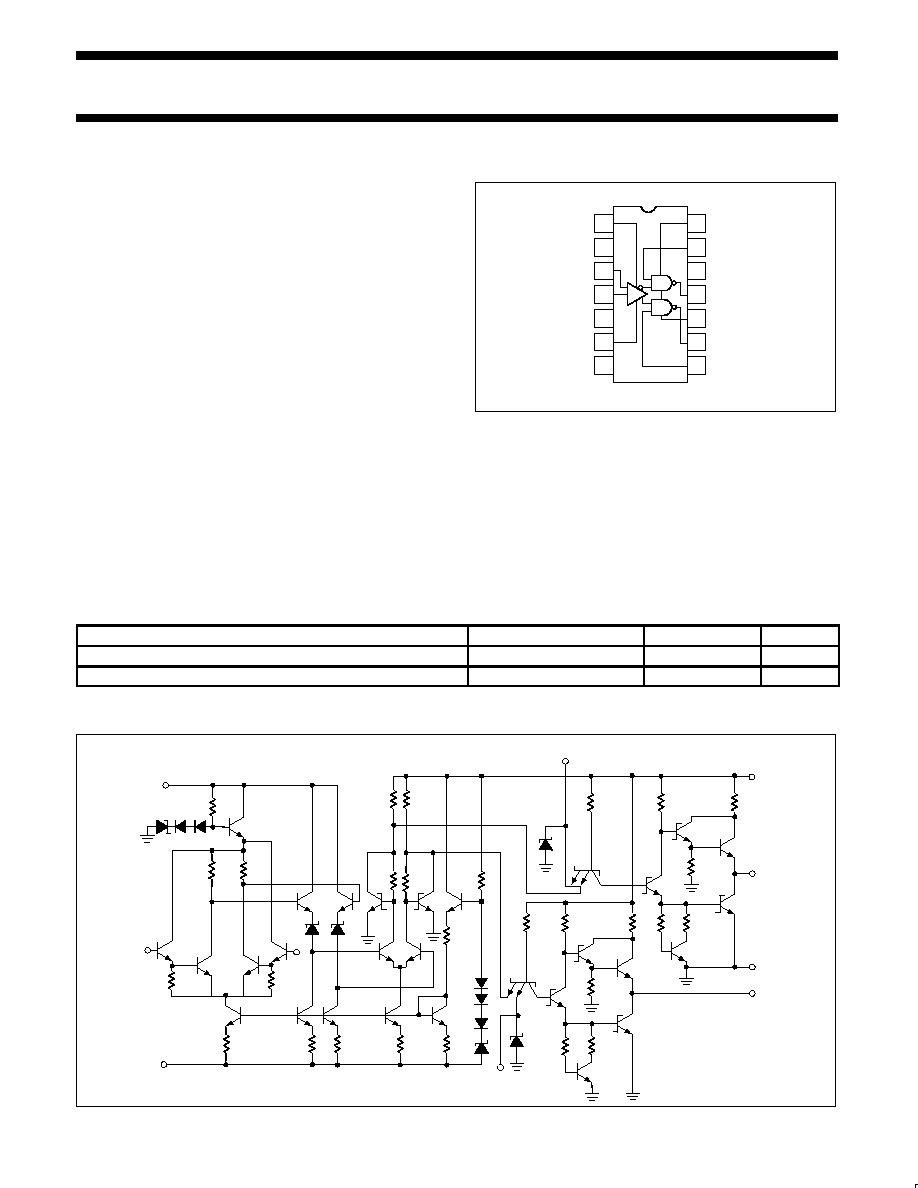
PIN CONFIGURATIONS
1
2
3
4
5
6
7
8
14
13
12
11
10
9
V1
+
NC
INPUT A
INPUT B
NC
V1
≠
NC
V2
+
STROBE A
OUTPUT A
NC
GND
OUTPUT B
STROBE B
D, N Packages
TOP VIEW
APPLICATIONS
∑
A/D conversion
∑
ECL-to-TTL interface
∑
TTL-to-ECL interface
∑
Memory sensing
∑
Optical data coupling
ORDERING INFORMATION
DESCRIPTION
TEMPERATURE RANGE
ORDER CODE
DWG #
14-Pin Plastic Dual In-Line Package (DIP)
0 to +70
∞
C
NE527N
0405B
14-Pin Small Outline (SO) Package
0 to +70
∞
C
NE527D
0175D
EQUIVALENT SCHEMATIC
V1
20K
1.5K
1.5K
INPUT A
INPUT
B
200
V1
300
300
100
200
750
750
6.13K
1K
1K
STROBE B
20K
4K
1.5K
STROBE A
4K
250
500
4K
55
250
500
GND
OUTPUT B
OUTPUT A
4K
1.5K
V2 +
55
7.5K
≠
7.5K
+

Philips Semiconductors Linear Products
Product specification
NE527
Voltage comparator
August 31, 1994
316
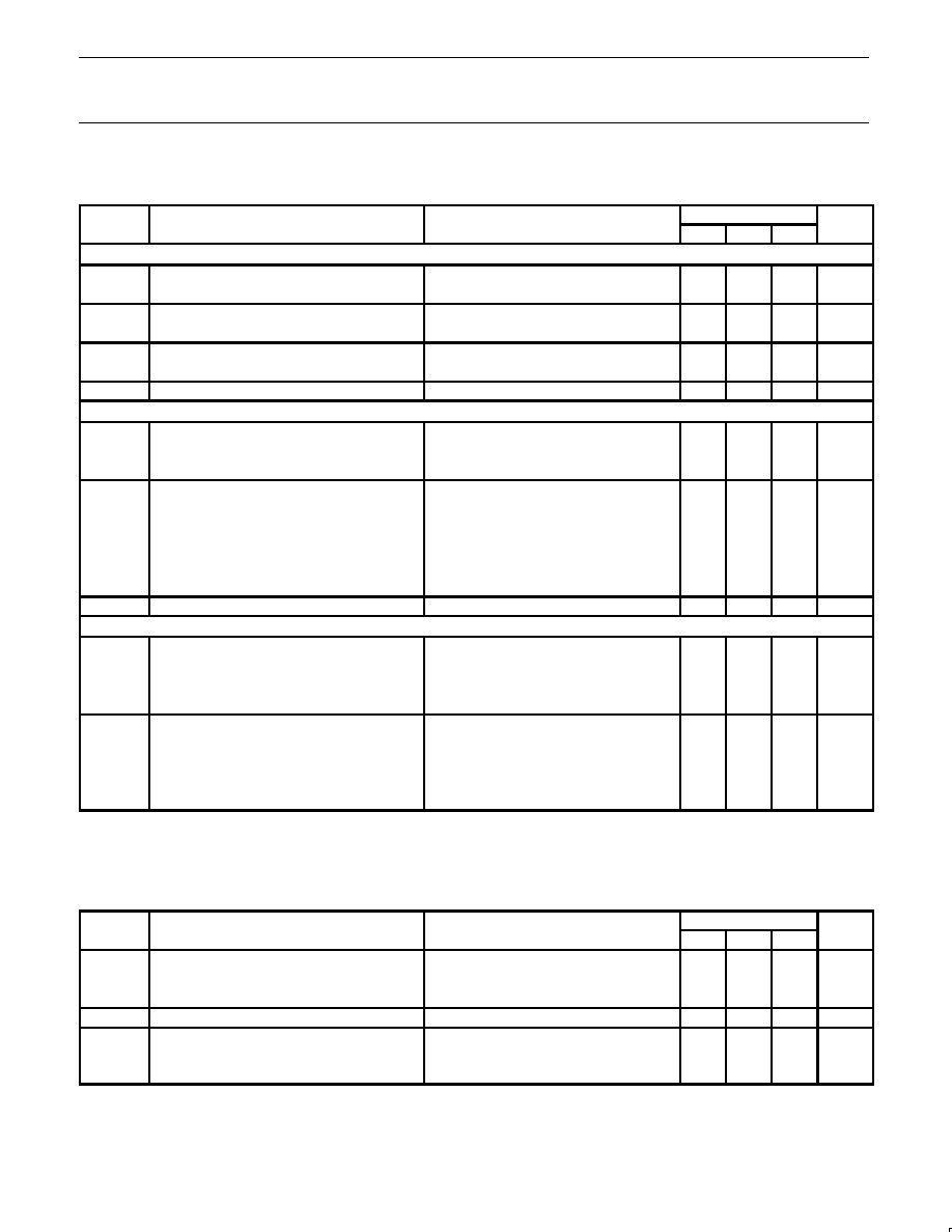
ABSOLUTE MAXIMUM RATINGS
SYMBOL
PARAMETER
RATING
UNIT
V
1
+
Positive supply voltage
+15
V
V
1
-
Negative supply voltage
-15
V
V
2
+
Gate supply voltage
+7
V
V
OUT
Output voltage
+7
V
V
IN
Differential input voltage
±
5
V
V
CM
Input common mode voltage
±
6
V
P
D
Max power dissipation
1
25
∞
C ambient (still air)
N package
1420
mW
D package
1040
mW
T
A
Operating temperature range
0 to +70
∞
C
T
STG
Storage temperature range
-65 to +150
∞
C
T
SOLD
Lead soldering temperature (10sec max)
+300
∞
C
NOTES:
1. Derate above 25
∞
C, at the following rates:
N package 11.4mW/
∞
C
D package 8.3mW/
∞
C
BLOCK DIAGRAM
V1
+
STROBE A
OUTPUT A
INPUT A
INPUT B
OUTPUT B
STROBE B
V1
≠
V2
+
Philips Semiconductors Linear Products
Product specification
NE527
Voltage comparator
August 31, 1994
317
DC ELECTRICAL CHARACTERISTICS
V1+=10V, V1-=-10V, V2+=+5.0V, unless otherwise specified.
SYMBOL
PARAMETER
TEST CONDITIONS
NE527
UNIT
SYMBOL
PARAMETER
TEST CONDITIONS
Min
Typ
Max
UNIT
Input characteristics
V
OS
Input offset voltage @ 25
∞
C
6
mV
V
OS
over temperature range
10
mV
I
BIAS
Input bias current @ 25
∞
C
2
µ
A
I
BIAS
over temperature range
4
µ
A
I
OS
Input offset current @ 25
∞
C
0.75
µ
A
I
OS
over temperature range
V
IN
=0V
1
µ
A
V
CM
Common-mode voltage range
-5
+5
V
Gate characteristics
V
OUT
Output Voltage
V
OUT
"1" State
V
2
+=4.75V, I
SOURCE
=-1mA
2.7
3.3
V
OUT
"0" State
V
2
+=4.75V, I
SINK
=10mA
0.5
V
Strobe inputs
"0" Input current
1
V
2
+=5.25V, V
STROBE
=0.5V
-2
mA
"1" Input current @ 25
∞
C
1
V
2
+=5.25V, V
STROBE
=2.7V
100
µ
A
Over temperature range
V
2
+=5.25V, V
STROBE
=2.7V
200
µ
A
"0" Input voltage
V
2
+=4.75V
0.8
V
"1" Input voltage
V
2
+=4.75V
2.0
V
I
SC
Short-circuit output current
V
2
+=5.25V, V
OUT
=0V
-18
-70
mA
Power supply requirements
Supply voltage
V
1
+
5
10
V
V
1
-
-6
-10
V
V
2
+
4.75
5
5.25
V
Supply current
V
1
+=10V, V
1
-=-10V
V
2
+=5.25V
I
1
+
Over temp.
5
mA
I
1
-
Over temp.
10
mA
I
2
+
Over temp.
20
mA
NOTES:
1. See Logic Function Table.
AC ELECTRICAL CHARACTERISTICS
T
A
=25
∞
C, unless otherwise specified. (See AC test circuit)
SYMBOL
PARAMETER
TEST CONDITIONS
LIMITS
UNIT
SYMBOL
PARAMETER
TEST CONDITIONS
Min
Typ
Max
UNIT
Transient response propagation delay time
t
PLH
Low-to-High
V
IN
=
±
100mV step
16
26
ns
t
PHL
High-to-Low
14
24
ns
Delay between output A and B
2
5
ns
Strobe delay time
t
ON
Turn-on time
6
ns
t
OFF
Turn-off time
6
ns

Philips Semiconductors Linear Products
Product specification
NE527
Voltage comparator
August 31, 1994
318
TYPICAL PERFORMANCE CHARACTERISTICS
OFFSET CURRENT
3.0
2.5
2.0
1.5
0
1.0
0.3
0.2
0.1
0
≠50
≠25
0
25
50
75 100 125
TEMPERATURE --
o
C
INOUR CURRENT --
A
µ
I2
+
V2
+ = 5.0V
V1
≠ = 10V
V1
+ = 10V
I1
≠
I1
+
15
14
13
7
6
5
4
3
2
≠50 ≠25
0
25
50
75
100
TEMPERATURE --
o
C
SUPPL
Y
CURRENT -- mA
V2
+ =
5.0V
TA = 25
o
C
160
150
140
130
120
110
100
5
6
7
8
9
10
SUPPLY VOLTAGE (V1
+, V1 ≠) -- VOLTS
POWER DISSIP
A
TION -- mW
TA = 25
o
C
V2
+ = 5.0V
T1
≠
T2
+
T1
+
8
7
6
5
4
3
2
1
0
5
6
7
8
9
10
SUPPL
Y
CURRENT -- mA
SUPPLY VOLTAGE (V1
+, V1 ≠) -- VOLTS
OUTPUT A
OUTPUT B
V1
+ = 10V, V1 ≠ = -- 10V
V2
+ = 5.0V
INPUT A
OVERDRIVE
5
4
3
2
1
0
+100
0
≠100
0
5
10
15
20
25
30
TIME -- ns
INPUT
VOL
T
AGE -- V
OUTPUT
VOL
T
AGE -- mV
V1
+ = 10V, V1 ≠ = -- 10V
V2
+ = 5.0V
OVERDRIVE
OVERDRIVE
INPUT B
OUTPUT A
5
4
3
2
1
0
+100
0
≠100
0
5
10
15
20
25
30
TIME -- ns
+
50mV
+
25mV
+
15mV
+
10mV
+
5mV
Input Currents vs Temperature
Supply Currents vs Temperature
Power Dissipation
vs Supply Voltage
Supply Current
vs Supply Voltage
Output Propagation Delays
Response Time for
Various Input Overdrives
INPUT
VOL
T
AGE -- V
OUTPUT
VOL
T
AGE -- mV
BIAS CURRENT
RESPONSE TIME TEST CIRCUIT
INPUT PROBE
500
INPUT
51
51
R1
+ 5
R2
+
.1
1
1K
13
3
4
R3
6
8
1K
(V1 +)
+10
10
µ
F
(V1 ≠)
≠10
.1
+5
10
9
11
.1
14
(V2 +)
+5
10
µ
F
+
OUTPUT
PROBE
+5
RL
5K
CR1
CR2
CR3
CR4
CL
NOTES:
CR1 -- CR4 = IN914
R1 selected for 15.1 divider
R2, 3 selected for 100mV at Pin 4
Input
PRR = 1MHz
Pw = 50ns
Tr = Tf = 2ns
Amplitude = 3.00V
Output
RL = 390
CL = 25pF (including
stray capacitance
Philips Semiconductors Linear Products
Product specification
NE527
Voltage comparator
August 31, 1994
319
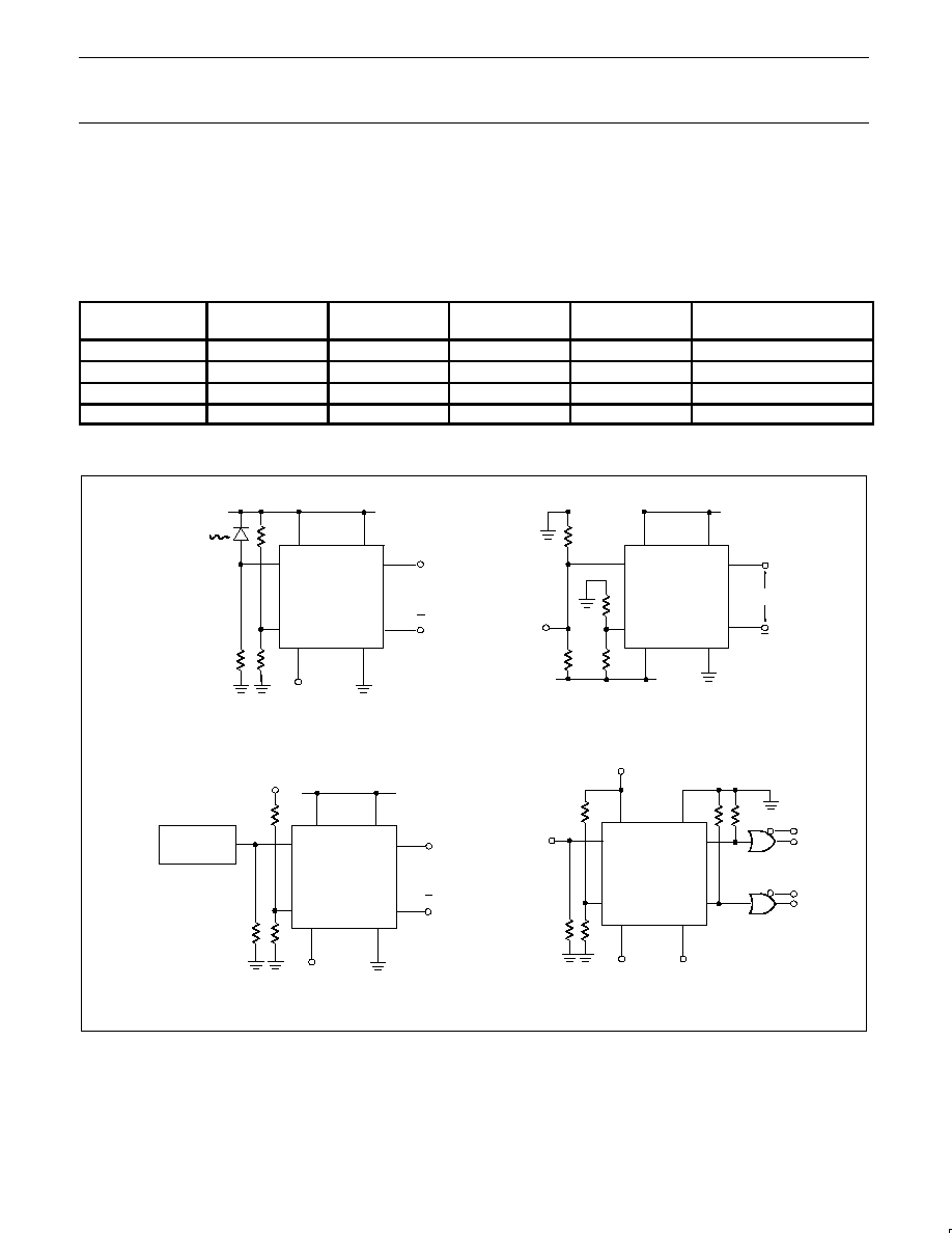
APPLICATIONS
One of the main features of the device is that supply voltages (V
1
+,
V
1
-) need not be balanced, as in the following diagrams. For proper
operation, however, negative supply (V
1
-) should always be at least
6V more than the ground terminal (Pin 6). Input common-mode
range should be limited to values of 2V less than the supply voltages
(V
1
+ and V
1
-) up to a maximum of
±
5V as supply voltages are
increased. It is also important to note that Output A is in phase with
Input A and Output B is in phase with Input B.
LOGIC FUNCTION
V
ID
(A
+
, B
≠
)
STROBE A
STROBE B
OUTPUT A
OUTPUT B
COMMENT
V
ID
-V
OS
H
X
L
H
Read I
IHA
, I
ILB
-V
OS
<V
ID
<V
OS
H
H
Undefined
Undefined
V
ID
V
OS
X
H
H
L
Read I
ILA
, I
IHB
X
L
L
H
H
TYPICAL APPLICATIONS
+ 5V
3
1
14
Q
Q
11
527N
9
10
6
4
R1
R1
R2
R2
ECL
INPUT
TTL OUTPUTS
≠ 10V
+ 5V
R2
3
1
14
Q
Q
11
529N
9
10
6
4
≠ 6V
R1
R2
3
1
14
Q
Q
11
527N
9
10
6
4
≠ 6V
R1
Q
Q
3
1
14
11
529N
9
10
6
4
3
1
14
11
527N
9
10
6
4
1103
MOS RAM
VREF
+ 5V
100
100
≠ 6V
3
1
14
11
529N
9
10
6
4
3
1
14
11
527N
9
10
6
4
+ 5V
TTL INPUT
3R1
R1
R1
≠ 10V
≠ 5.2V
2K
2K
Photodiode Detector
ECL≠to≠TTL Interface
MOS Memory Sense AMP
TTL≠to≠ECL Interface