 | –≠–ª–µ–∫—Ç—Ä–æ–Ω–Ω—ã–π –∫–æ–º–ø–æ–Ω–µ–Ω—Ç: NE531N | –°–∫–∞—á–∞—Ç—å:  PDF PDF  ZIP ZIP |

Philips Semiconductors Linear Products
Product specification
NE/SE531
High slew rate operational amplifier
70
August 31, 1994
853-0809 13721
DESCRIPTION
The 531 is a fast slewing high performance operational amplifier
which retains DC performance equal to the best general purpose
types while providing far superior large-signal AC performance. A
unique input stage design allows the amplifier to have a large-signal
response nearly identical to its small-signal response. The amplifier
is compensated for truly negligible overshoot with a single capacitor.
In applications where fast settling and superior large-signal
bandwidths are required, the amplifier out-performs conventional
designs which have much better small-signal response. Also,
because the small-signal response is not extended, no special
precautions need be taken with circuit board layout to achieve
stability. The high gain, simple compensation, and excellent stability
of this amplifier allow its use in a wide variety of instrumentation
applications.
FEATURES
∑
35V/
µ
s slew rate at unity gain
∑
Pin-for-pin replacement for
µ
A709,
µ
A748, or LM101
∑
Compensated with a single capacitor
PIN CONFIGURATIONS
1
2
3
4
5
6
7
8
≠
+
OFFSET NULL
INVERTING INPUT
NON≠INVERTING INPUT
V≠
FREQ. COMP.
V+
OUTPUT
OFFSET
N, FE Packages
∑
Same low drift offset null circuitry as
µ
A741
∑
Small-signal bandwidth 1MHz
∑
Large-signal bandwidth 500kHz
∑
True op amp DC characteristics make the 531 the ideal answer to
all slew rate limited operational amplifier applications
ORDERING INFORMATION
DESCRIPTION
TEMPERATURE RANGE
ORDER CODE
DWG #
8-Pin Plastic Dual In-Line Package (DIP)
0 to +70
∞
C
NE531N
0404B
8-Pin Ceramic Dual In-Line Package (CERDIP)
-55
∞
C to +125
∞
C
SE531FE
0580A
8-Pin Ceramic Dual In-Line Package (CERDIP)
0
∞
C to +70
∞
C
NE531FE
0580A
ABSOLUTE MAXIMUM RATINGS
SYMBOL
PARAMETER
RATING
UNIT
V
S
Supply voltage
±
22
V
P
D MAX
Maximum power dissipation
T
A
=25
∞
C (still-air)
1
FE package
780
mW
N package
1160
mW
Differential input voltage
±
15
V
V
CM
Common-mode input voltage
2
±
15
V
Voltage between offset null and V-
±
0.5
V
T
A
Operating ambient temperature range
NE531
0 to +70
∞
C
SE531
-55 to +125
∞
C
T
STG
Storage temperature range
-65 to +150
∞
C
T
SOLD
Lead soldering temperature (10sec max)
300
∞
C
Output short-circuit duration
3
indefinite
NOTES:
1. The following derating factors should be applied above 25
∞
C:
FE package at 6.2mW/
∞
C
N package at 9.3mW/
∞
C
2. For supply voltages less than
±
15V, the absolute maximum input voltage is equal to the supply voltage.
3. Short-circuit may be to ground or either supply. Rating applies to +125
∞
C case temperature or to +75
∞
C ambient temperature.
Philips Semiconductors Linear Products
Product specification
NE/SE531
High slew rate operational amplifier
August 31, 1994
71
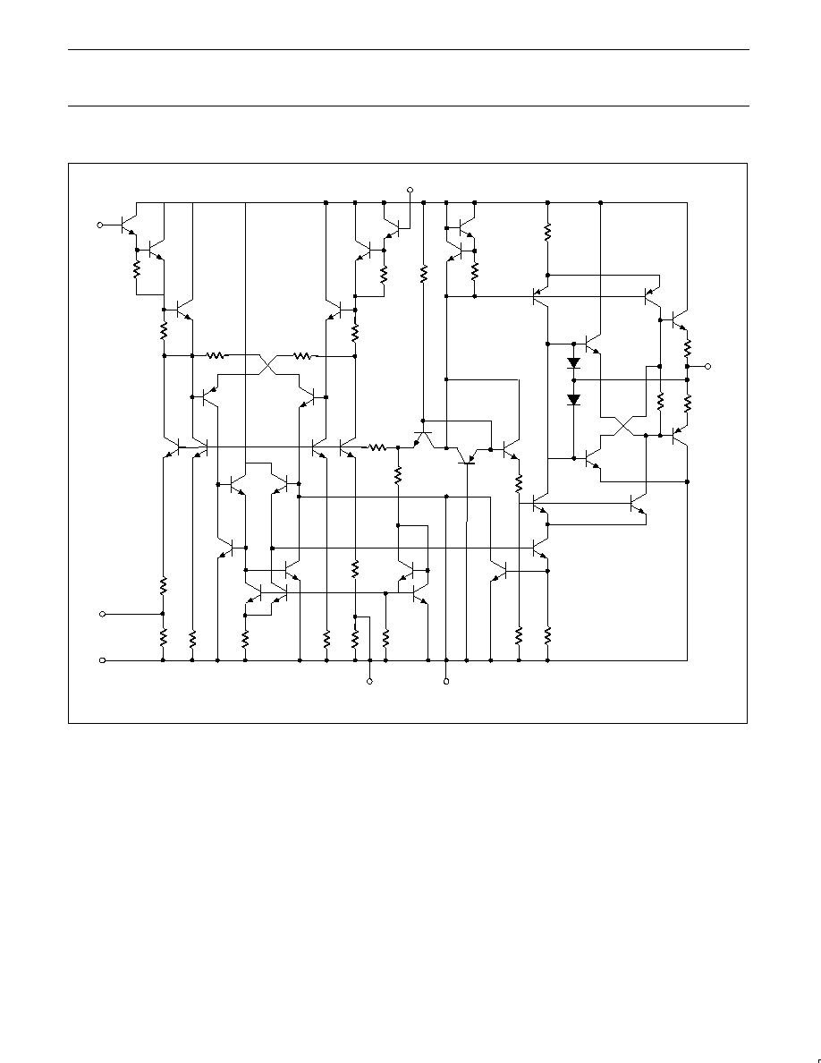
EQUIVALENT SCHEMATIC
INPUT
2
Q1
Q2
R1
Q3
R2
.2
R3
2.2
Q7
Q9
Q10
R8
2.2
Q6
R5
.2
Q5
Q6
R4
R15
100
Q20
Q19
R14
10
R20
.33
Q23
Q27
Q38
Q37
Q29
Q22
Q35
Q21
R16
10
Q11
Q12
R18
.33
Q28
Q25
R24
.04
OUTPUT
R22
3.3
R28
.04
Q30
Q32
Q31
R17
10
Q33
Q34
Q24
Q23
R10
6.5
R21
.2
R27
6.5
R13
1.6
5
6
OFFSET ADJUST
FREQUENCY
COMPENSATION
Q13 Q14
Q15
R7
6.5
R11
1.5
R8
7.8
R12
.17
Q17
Q18
Q19
R9
1.8
INPUT
3
+
OFFSET
ADJUST
1
4
V
R10
6.5
q8
Philips Semiconductors Linear Products
Product specification
NE/SE531
High slew rate operational amplifier
August 31, 1994
72
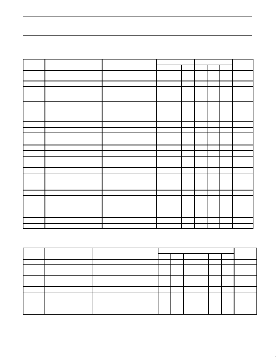
DC ELECTRICAL CHARACTERISTICS
V
S
=
±
15V, unless otherwise specified.
SYMBOL
PARAMETER
TEST CONDITIONS
SE531
NE531
UNIT
SYMBOL
PARAMETER
TEST CONDITIONS
Min
Typ
Max
Min
Typ
Max
UNIT
V
OS
Offset voltage
R
S
10k
, T
A
=25
∞
C
R
S
310k
, over temp
2.0
5.0
6.0
2.0
6.0
7.5
mV
mV
V
OS
Over temp
10
10
µ
V/
∞
C
I
OS
Offset current
T
A
=25
∞
C
T
A
=High
T
A
=Low
30
200
200
500
50
200
200
300
nA
nA
nA
I
OS
Over temp
0.4
0.4
nA/
∞
C
I
BIAS
Input bias current
T=25
∞
C
T
A
=High
T
A
=Low
300
500
500
1500
400
1500
1500
2000
nA
nA
nA
I
BIAS
Over temp
2
2
nA/
∞
C
V
CM
Common-mode voltage range
T
A
=25
∞
C
±
10
±
10
V
CMRR
Common-mode rejection ratio
T
A
=25
∞
C,
R
S
10k
70
100
dB
Over temp R
S
10k
70
90
dB
R
IN
Input resistance
T
A
=25
∞
C
20
20
M
V
OUT
Output voltage swing
R
L
10k
, over temp
±
10
±
13
±
10
±
13
V
I
CC
Supply current
T
A
=25
∞
C
7.0
10
mA
T
MAX
7.0
10
mA
P
D
Power consumption
T
A
=25
∞
C
210
300
mW
R
S
10k
, T
A
=25
∞
C
10
150
µ
V/V
PSRR
Power supply rejection ratio
R
S
10k
, over temp
10
150
µ
V/V
R
OUT
Output resistance
T
A
=25
∞
C
75
75
T
A
=25
∞
C,
R
L
10k
, V
OUT
=
±
10V
50
100
20
60
V/mV
A
VOL
Large-signal voltage gain
R
L
10k
, V
OUT
=
±
10V,
over temp
25
15
V/mV
V
INN
Input noise voltage
25
∞
C f=1kHz
20
20
nV/
Hz
I
SC
Short-circuit current
25
∞
C
5
15
45
5
15
45
mA
AC ELECTRICAL CHARACTERISTICS
T
A
=25
∞
C V
S
=+15V, unless otherwise specified.
1
SYMBOL
PARAMETER
TEST CONDITIONS
SE531
NE531
UNIT
SYMBOL
PARAMETER
TEST CONDITIONS
Min
Typ
Max
Min
Typ
Max
UNIT
BW
Full power bandwidth
500
500
kHz
t
S
Settling time (1%)
(0.1%)
A
V
=+1, V
IN
=
±
10V
1.5
2.5
1.5
2.5
µ
s
µ
s
Large-signal overshoot
A
V
=+1, V
IN
=
±
10V
2
2
%
Small-signal overshoot
A
V
=+1, V
IN
=400mV
5
5
%
t
R
Small-signal rise time
A
V
=+1, V
IN
=400mV
300
300
ns
SR
Slew rate
A
V
=100
35
35
V/
µ
s
A
V
=10
35
35
V/
µ
s
A
V
=1 (non-inverting)
20
30
30
V/
µ
s
A
V
=1 (inverting)
25
35
35
V/
µ
s
NOTES:
1. All AC testing is performed in the transient response test circuit.

Philips Semiconductors Linear Products
Product specification
NE/SE531
High slew rate operational amplifier
August 31, 1994
73
TEST LOAD CIRCUITS
Offset Null Circuit
Transient Response Circuit
2
V+
≠
7
3
4
+
1
5
10K
6
V≠
EIN
2
V+
100pF
7
8
3
4
≠
+
50
V≠
51
EOUT
2K
30pf
TYPICAL PERFORMANCE CHARACTERISTICS
V
S
= +15V, T
A
= +255C, unless otherwise specified.
TEMPERATURE - C
≠20
160
140
120
100
80
60
40
20
0
≠60
20
60
100
140
TEMPERATURE - C
INPUT OFFSET CURRENT -nA
1000
800
600
400
200
0
INPUT BIAS CURRENT -nA
≠20
≠60
20
60
100
140
120
110
100
90
80
5
10
15
20
25
SUPPLY VOLTAGE ≠ +V
INPUT BIAS CURRENT ≠ nA
AV = 1000,
Ri = 50
CC = 2pF
C
C
OUT
V
Rf =
50k
Ri
AV = 100, Ri = 5000
CC = 2pF
AV = 10, Ri = 5.50
,
CC = 10pF
AV = 10, Ri = 00,0
+60
+50
+40
+30
+20
+10
0
≠10
10K
100K
1M
10M
FREQUENCY ≠ Hz
VOL
T
AGE DRAIN ≠ dB
GAIN
CC = 100PF
PHASE
PHASE IN DEGREES
VOL
T
AGE GAIN -- dB
0
15
30
45
60
75
90
105
120
135
150
165
180
120
110
100
90
80
70
60
50
40
30
20
10
0
1
10
100
1K
10K 100K 1M
10M
FREQUENCY ≠ Hz
CONSUMPTION --mW
300
275
250
225
200
175
150
125
100
75
50
5V
10
15
20
25
SUPPLY VOLTAGE -- +V
+
≠
531
Input Offset Curent as a Function
of Ambient Temperature
Input Bias Curent as a Function
of Ambient Temperature
Input Bias Curent as a Function
of Supply Voltage
Closed Loop Non-Inverting Voltage Gain
as a Function of Frequency
Open-Loop Phase Response and
Voltage Gain as a Function of
Ambient Temperature
Power Consumption as a Function
of Supply Voltage
Philips Semiconductors Linear Products
Product specification
NE/SE531
High slew rate operational amplifier
August 31, 1994
74
TYPICAL PERFORMANCE CHARACTERISTICS
(Continued)
V
S
= +15V, T
A
= 25
∞
C, unless otherwise specified.
250
200
150
100
50
≠60
≠20
+20
+60
+100
+140
POWER CONSUMPTION -- mW
TEMPERATURE -- C
o
0
115
110
100
95
90
85
80
5
10
15
20
V VOL
T
AGE GAIN --dB
L
SUPPLY VOLTS -- +V
+15
+10
+5
0
≠5
≠10
≠15
5
10
15
SUPPLY VOLTAGE -- +V
OUTPUT SWING -- VOL
TS
COMMON MODE RANGE -- V
+15
+10
+5
0
≠5
≠10
≠15
5
10
15
SUPPLY VOLTAGE -- +V
20
27
24
21
18
12
9
6
3
0
1K
3K
10K
30K
100K
300K
1M
PEAK≠T
O≠PEAK OUTPUT SWING -- V
+
≠
531
100pF
IN
2K
OUT
FREQUENCY, Hz
+
≠
531
100pF
IN
30Pf
OUT
2K
+10
+5
0
≠5
≠10
OUTPUT VOL
T
AGE -- V
0
500 1000 1500 2000 2500 3000 3500
TIME -- nsec
+
≠
531
100pF
IN
OUT
VIN = 400mV
90%
10%
500
400
300
200
100
0
0
200
400
600
800
1000
1200
1400
TIME -- nsec
OUTPUT VOL
T
AGE --mV
+
≠
531
IN
OUT
10K
50pF
5K
10K
+15
+10
+5
0V
≠5
≠10
≠15
0
0.5
1.0
1.5
2.0
2.5
3.0
3.5
4.0
TIME --
µ
sec
OUTPUT VOL
T
AGE -- V
Power Consumption
as a Function of Ambient Temperature
Open-Loop Voltage Gain as a
Function of Supply Voltage
Output Voltage Swing as a Function
of Supply Voltage
Input Voltage Range
as a Function of Supply Voltage
Output Voltage Swing as a
Function of Frequency
Voltage Follower
Large-Signal Response
Unity Gain Inverting Amplifier Large-Signal
Response Function of Frequency
Voltage Follower
Transient Response

Philips Semiconductors Linear Products
Product specification
NE/SE531
High slew rate operational amplifier
August 31, 1994
75
TYPICAL APPLICATIONS
High-Speed Inverter
(10MHz Bandwidth)
Pulse Response
High-Speed Inverter
Fast Settling Voltage-Follower
Large-Signal Response Voltage-Follower
Three-Pole Active Low-Pass Filter Butterworth
Maximally Flat Response
1
Response of 3-Pole Active
Butterworth Maximally Flat Filter
2pf
IN
10K
10K
5.1K
V+
531
30pf
OUT
4.7K
V≠
fo
100pF
531
+
≠
IN
OUT
30K
10K
10K
531
.0032
.056
10K
.022
100pF
f0 ≠ 1KHz
0.5V/DIV
200nsec/DIV
2V/DIV
0.5
µ
s/DIV
f = 500KHz
60dB/DECADE
0
≠5
≠10
≠15
≠20
≠25
100
300
1K
3K
10K
FREQUENCY -- Hz
A
TTENUA
TION -- dB

Philips Semiconductors Linear Products
Product specification
NE/SE531
High slew rate operational amplifier
August 31, 1994
76
TYPICAL APPLICATIONS
(Continued)
531
IN
a. Half-Wave
b. Full-Wave
Precision Rectifiers
AC Millivoltmeter
Sample-and-Hold
531
100pF
IN
10K
10K
OUT
5.1K
+
≠
10K
531
100K
100K
531
+
≠
100pF
DIODES
IN914
1
µ
F
M
RE
IN
1%
10K
100pF
5.1K
≠
+
≠
+
531
100PF
10K 1%
OUT
SIGNAL
IN
18K
330pF
470
33K
IN457
IN/51A
≠
+
LOGIC IN
300K
15MSEC
Q1
ZN3819
Q2
3N128
100K
.0047
CDE#
CD19
FD4725
30K
10K
≠15
≠15
+15
IN457
OUTPUT
531
≠
+
Philips Semiconductors Linear Products
Product specification
NE/SE531
High slew rate operational amplifier
August 31, 1994
77
CYCLIC A-TO-D CONVERTER
One interesting, but much ignored, A/D converter is the cyclic
converter. This consists of a chain of identical stages, each of which
senses the polarity of the input. The stage then subtracts V
REF
from
the input and doubles the remainder if the polarity was correct. In
Figure 1, the signal is full-wave rectified and the remainder of
V
IN
-V
REF
is doubled. A chain of these stages gives the gray code
equivalent of the input voltage in digitized form related to the
magnitude of V
REF
. Possessing high potential accuracy, the circuit
using NE531 devices settles in 5
µ
s.
TRIANGLE AND SQUARE WAVE GENERATOR
The circuit in Figure 2 will generate precision triangle and square
waves. The output amplitude of the square wave is set by the output
swing of op amp A-1, and R1/R2 sets the triangle amplitude. The
frequency of oscillation in either case is:
f
+
1
4RC
@
R2
R1
(1)
The square wave will maintain 50% duty cycle even if the amplitude
of the oscillation is not symmetrical.
The use of the NE531 in this circuit will allow good square waves to
be generated to quite high frequencies. Since the amplifier A1 runs
open-loop, there is no need for compensation. The
triangle-generating amplifier must be compensated. The NE5535
device can be used as well, except for the lower frequency
response.
a.
b.
+vcc
10K
LOGIC OUT
NE531
+
≠
10K
2K
VREF
NE531
+
≠
20K
20K
VOUT
VREF
≠VIN
LOGOUT
VIN
VREF
VREF
VIN
0
Figure 1. Cyclic A-to-D Converter