 | –≠–ª–µ–∫—Ç—Ä–æ–Ω–Ω—ã–π –∫–æ–º–ø–æ–Ω–µ–Ω—Ç: NE5521 | –°–∫–∞—á–∞—Ç—å:  PDF PDF  ZIP ZIP |
Philips Semiconductors Linear Products
Product specification
NE/SA/SE5521
LVDT signal conditioner
901
August 31, 1994
853-0043 13721
DESCRIPTION
The NE/SA/SE5521 is a signal conditioning circuit for use with
Linear Variable Differential Transformers (LVDTs) and Rotary
Variable Differential Transformers (RVDTs). The chip includes a low
distortion, amplitude-stable sine wave oscillator with programmable
frequency to drive the primary of the LVDT/RVDT, a synchronous
demodulator to convert the LVDT/RVDT output amplitude and phase
to position information, and an output amplifier to provide
amplification and filtering of the demodulated signal.
FEATURES
∑
Low distortion
∑
Single supply 5V to 20V, or dual supply
±
2.5V to
±
10V
∑
Oscillator frequency 1kHz to 20kHz
∑
Capable of ratiometric operation
∑
Low power consumption (182mV typ)
APPLICATIONS
∑
LVDT signal conditioning
∑
RVDT signal conditioning
∑
LPDT signal conditioning
∑
Bridge circuits
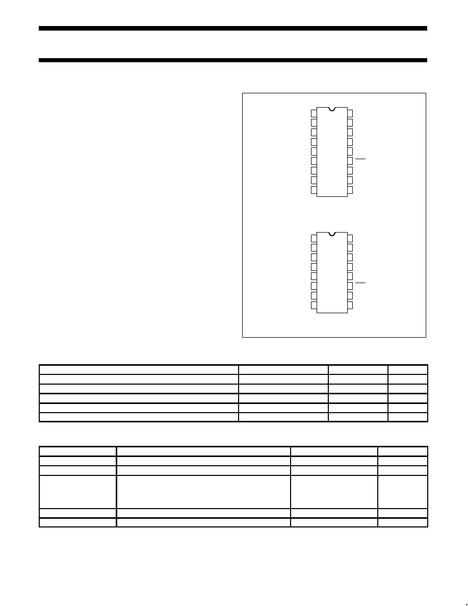
PIN CONFIGURATIONS
1
2
3
4
5
6
7
8
9
10
11
12
13
14
16
15
1
2
3
4
5
6
7
8
11
12
13
14
15
16
18
17
9
10
AMP OUT
+IN
≠IN
LVDT IN
DEMOD OUT
SYNC
GND
N.C.
N.C.
V+
CT
VREF
FEEDBACK
OSC
OSC
VREF/2
RT
N.C.
AMP OUT
+IN
≠IN
LVDT IN
DEMOD OUT
SYNC
GND
N.C.
V+
CT
VREF
FEEDBACK
OSC
OSC
VREF/2
RT
F, N Packages
TOP VIEW
D
1
Package
TOP VIEW
NOTE:
1. SOL -- released in large SO package only.
ORDERING INFORMATION
DESCRIPTION
TEMPERATURE RANGE
ORDER CODE
DWG #
18-Pin Plastic Dual In-Line Package (DIP)
0 to +70
∞
C
NE5521N
0407A
16-Pin Small Outline Large (SOL) Package
0 to +70
∞
C
NE5521D
0171B
18-Pin Plastic Dual In-Line Package (DIP)
≠40 to +85
∞
C
SA5521N
0407A
18-Pin Ceramic Dual In-Line Package (CERDIP)
≠55 to +125
∞
C
SE5521F
0583A
16-Pin Ceramic Dual In-Line Package (CERDIP)
≠40 to +85
∞
C
SA5521D
0582B
ABSOLUTE MAXIMUM RATINGS
SYMBOL
PARAMETER
RATING
UNIT
V
CC
Supply voltage
+20
V
Split supply voltage
±
10
V
T
A
Operating temperature range
NE5521
SA5521
SE5521
0 to 70
≠40 to +85
≠55 to +125
∞
C
∞
C
∞
C
T
STG
Storage temperature range
≠65 to +125
∞
C
P
D
Power dissipation
1
910
mW
NOTES:
1. For derating, see typical power dissipation versus load curves (Figure 1).
Philips Semiconductors Linear Products
Product specification
NE/SA/SE5521
LVDT signal conditioner
August 31, 1994
902
BLOCK DIAGRAM
NOTE:
Pin numbers are for F, N packages.
16
17
11
18
3
2
1
5
15
13
14
12
7
4
6
OSC
AUX AMP
DOMOD OUT
SINE
CONV
10k
10k
10k
10k
≠
+
FEEDBACK
OSC
GND/V≠
LVDT IN
SYNC
≠
+
≠
+
VREF
VREF/2
OSC
CT
RT
V+
≠IN
+IN
AMP
OUT
SYNCHRONOUS
DEMODULATOR
PIN DEFINITIONS FOR D, F AND N PACKAGES
PIN NO.
SYMBOL
DEFINITION
D
F, N
SYMBOL
DEFINITION
1
1
Amp Out
Auxiliary Amplifier Out.
2
2
+IN
Auxiliary Amplifier non-inverting input.
3
3
≠IN
Auxiliary Amplifier inverting input.
4
4
LVDT IN
Input to Synchronous Demodulator from the LVDT/RVDT secondary.
5
5
DEMOD OUT
Pulsating DC output from the Synchronous Demodulator output. This voltage should be filtered before
use.
6
6
SYNC
Synchronizing input for the Synchronizing Demodulator. This input should be connected to the OSC or
OSC output. Sync is referenced to V
REF
/2.
7
7
GND
Device return. Should be connected to system ground or to the negative supply.
8
8
NC
No internal connection.
--
9
NC
No internal connection.
--
10
NC
No internal connection.
9
11
R
T
A temperature stable 18k
resistor should be connected between this pin and Pin 7.
10
12
V
REF
/2
A high impedance source of one half the potential applied to V
REF
. The LVDT/RVDT secondary return
should be to this point. A bypass capacitor with low impedance at the oscillator frequency should also be
connected between this pin and ground.
11
13
OSC
Oscillator sine wave output that is 180
∞
out of phase with the OSC signal. The LVDT/RVDT primary is
usually connected between OSC and OSC pins.
12
14
OSC
Oscillator sine wave output. The LVDT/RVDT primaries are usually connected between OSC and OSC
pins.
13
15
FEEDBACK
Usually connected to the OSC output for unity gain, a resistor between this pin and OSC, and one be-
tween this pin and ground can provide for a change in the oscillator output pin amplitudes.
14
16
V
REF
Reference voltage input for the oscillator and sine converter. This voltage MUST be stable and must not
exceed +V supply voltage.
15
17
C
T
Oscillator frequency-determining capacitor. The capacitor connected between this pin and ground should
be a temperature-stable type.
16
18
+V
Positive supply connection.
Philips Semiconductors Linear Products
Product specification
NE/SA/SE5521
LVDT signal conditioner
August 31, 1994
903
DC ELECTRICAL CHARACTERISTICS
V+ = V
REF
= 10V, T
A
= 0 to 70
∞
C for NE5521, T
A
= ≠55 to +125
∞
C for SE5521, T
A
= ≠40 to 85
∞
C for SA5521, Frequency = 1kHz, unless
otherwise noted.
SYMBOL
PARAMETER
TEST CONDITIONS
NE5521
SA/SE5521
UNIT
SYMBOL
PARAMETER
TEST CONDITIONS
Min
Typ
Max
Min
Typ
Max
UNIT
V
CC
Supply current
12.9
20
12.9
18
mA
I
REF
Reference current
5.3
8
5.3
8
mA
V
REF
Reference voltage range
5
V+
5
V+
V
P
D
Power dissipation
182
280
182
260
mW
Oscillator Section
Oscillator output
R
L
= 10k
V
REF
8.8
V
REF
8.8
V
RMS
THD
Sine wave distortion
No load
1.5
1.5
%
Initial amplitude error
T
A
= 25
∞
C
0.4
±
3
0.4
±
3
%
Tempco of amplitude
0.005
0.01
0.005
0.01
%/
∞
C
Init. accuracy of oscillator freq.
T
A
= 25
∞
C
±
0.9
±
5
±
0.9
±
5
%
Temperature coeff. of frequency
1
0.05
0.05
%/
∞
C
Voltage coeff. of frequency
2.5
3.3
%/V(V
REF
)
Min OSC (OSC) Load
2
300
170
300
170
Demodulator Section
r
Linearity error
5V
P-P
input
±
0.05
±
0.1
±
0.05
±
0.1
%FS
Maximum demodulator input
V
REF
2
V
REF
2
V
P-P
V
OS
Demodulator offset voltage
±
1.4
±
5
±
1.4
±
5
mV
TCV
OS
Demodulator offset voltage drift
5
25
5
25
µ
V/
5
C
I
BIAS
Demodulator input current
≠600
≠234
≠500
≠234
nA
V
R/2
accuracy
±
0.1
±
1
±
0.1
±
1
%
Auxiliary Output Amplifier
V
OS
Input offset voltage
±
0.5
±
5
±
0.5
±
5
mV
I
BIAS
Input bias current
≠600
≠210
≠500
≠210
nA
I
OS
Input offset current
10
50
10
50
nA
A
V
Gain
100
385
100
385
V/mV
SR
Slew rate
1.3
1.3
V/
µ
s
GBW
Unity gain bandwidth product
A
V
= 1
1.6
1.6
MHz
Output voltage swing
R
L
= 10k
7
8.2
7
8.2
V
Output short circuit current to
ground or to V
CC
T
A
= 25
∞
C
42
100
42
100
mA
NOTES:
1. This is temperature coefficient of frequency for the device only. It is assumed that C
T
and R
T
are fixed in value and C
T
leakage is fixed over
the operating temperature range.
2. Minimum load impedance for which distortion is guaranteed to be less than 5%.
Philips Semiconductors Linear Products
Product specification
NE/SA/SE5521
LVDT signal conditioner
August 31, 1994
904
DEFINITION OF TERMS
Oscillator Output
RMS value of the AC voltage at the oscillator output pin. This output is referenced to V
REF/2
and is a function of V
REF
.
Sine Wave Distortion
The Total Harmonic Distortion (THD) of the oscillator output with no load. This is not a
critical specification in LVDT/RVDT systems. This figure could be 15% or more without
affecting system performance.
Initial Amplitude Error
A measure of the interchangeability of NE/SA/SE5521 parts, not a characteristic of any one
part. It is the degree to which the oscillator output of a number of NE/SA/SE5521 samples
will vary from the median of that sample.
Initial Accuracy of Oscillator Frequency
Another measure of the interchangeability of individual NE/SA/SE5521 parts. This is the
degree to which the oscillator frequency of a number of NE/SA/SE5521 samples will vary
from the median of that sample with a given timing capacitor.
Tempco of Oscillator Amplitude
A measure of how the oscillator amplitude varies with ambient temperature as that
temperature deviates from a 25
∞
C ambient.
Tempco of Oscillator Frequency
A measure of how the oscillator frequency varies with ambient temperature as that
temperature deviates from a 25
∞
C ambient.
Voltage Coefficient of Oscillator Frequency
The degree to which the oscillator frequency will vary as the reference voltage (V
REF
)
deviates from +10V.
Min OSC (OSC) Load
Minimum load impedance for which distortion is guaranteed to be less than 5%.
Linearity Error
The degree to which the DC output of the demodulator/amplifier combination matches a
change in the AC signal at the demodulator input. It is measured as the worst case
nonlinearity from a straight line drawn between positive and negative fullscale end points.
Maximum Demodulator Input
The maximum signal that can be applied to the demodulator input without exceeding the
specified linearity error.
APPLICATION INFORMATION
OSC frequency
+
V
REF
*
1.3V
V
REF
(R
T
)
1.5k) C
T
Figure 1. Device Power Dissipation vs OSC ≠ OSC Load at +25
∞
C
2000
1000
800
700
600
500
400
300
200
100
0.2
0.4
0.6
0.8
1 2
3
DEVICE POWER DISSIP
A
TION (mW)
OSC≠OSC LOAD (k
)
5V
15V
10V
VREF = V+ = 20V
PDMAX (SO PACKAGE)
PDMAX (N PACKAGE)
AT TA = 70
∞
C, TJ(MAX) = +150
∞
C
AT TA = +85
∞
C, TJ(MAX) = +150
∞
C
PDMAX (F PACKAGE)
PDMAX (F PACKAGE)
AT TA = +125
∞
C, TJ(MAX) = +165
∞
C
AT TA = +125
∞
C, TJ(MAX) = +150
∞
C

Philips Semiconductors Linear Products
Product specification
NE/SA/SE5521
LVDT signal conditioner
August 31, 1994
905
Figure 2. Oscillator Frequency Variation With Voltage
(Normalized to V
REF
= V
CC
= 10V) T
A
= +25
∞
C
16
8
0
≠8
≠16
5
8
10
12
14
16
18
20
VCC = VREF (V)
fOSC
(%)
I(mA)
Figure 3. I
REF
and I
CC
vs Voltage (T
A
= +25
∞
C)
20
15
10
5
0
5
10
15
20
25
VCC = VREF (V)
IREF
ICC
I(mA)
Figure 4. I
REF
and I
CC
vs Temperature
(V
REF
= V
CC
= 10V)
16
14
12
10
8
6
4
≠55
≠40
0
25
70 85 125
TA (
∞
C)
IREF
ICC