 | –≠–ª–µ–∫—Ç—Ä–æ–Ω–Ω—ã–π –∫–æ–º–ø–æ–Ω–µ–Ω—Ç: NE5537D | –°–∫–∞—á–∞—Ç—å:  PDF PDF  ZIP ZIP |
Philips Semiconductors Linear Products
Product specification
NE/SE5537
Sample-and-hold amplifier
884
August 31, 1994
853-1044 13721
DESCRIPTION
The NE5537 monolithic sample-and-hold amplifier combines the
best features of ion-implanted JFETs with bipolar devices to obtain
high accuracy, fast acquisition time, and low droop rate. This device
is pin-compatible with the LF198, and features superior performance
in droop rate and output drive capability. The circuit shown in Figure
1 contains two operational amplifiers which function as a unity gain
amplifier in the sample mode. The first amplifier has bipolar input
transistors which give the system a low offset voltage. The second
amplifier has JFET input transistors to achieve low leakage current
from the hold capacitor. A unique circuit design for leakage current
cancellation using current mirrors gives the NE5537 a low droop
rate at higher temperature. The output stage has the capability to
drive a 2k
load. The logic input is compatible with TTL, PMOS or
CMOS logic. The differential logic threshold is 1.4V with the sample
mode occurring when the logic input is high. It is available in 8-lead
TO-5, 8-pin plastic DIP packages, and 14-pin SO packages.
FEATURES
∑
Operates from
±
5V to
±
18V supplies
∑
Hold leakage current 6pA @ T
J
= 25
∞
C
∑
Less than 4
µ
s acquisition time
∑
TTL, PMOS, CMOS compatible logic input
∑
0.5mV typical hold step at CH=0.01
µ
F
∑
Low input offset: 1MV (typical)
∑
0.002% gain accuracy with R
L
=2k
∑
Low output noise in hold mode
∑
Input characteristics do not change during hold mode
∑
High supply rejection ratio in sample or hold
∑
Wide bandwidth
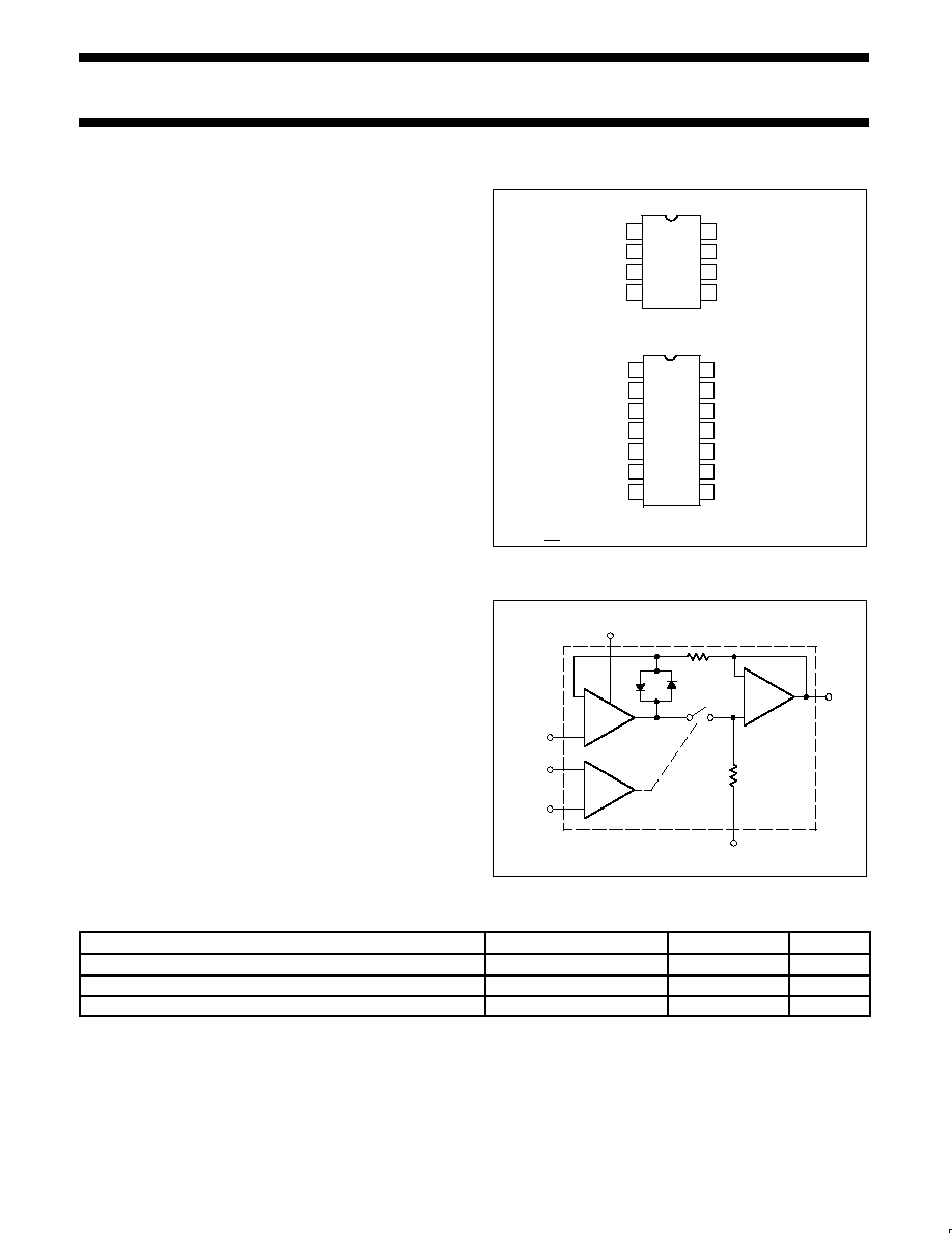
PIN CONFIGURATIONS
FE and N Packages
D
1
Package
NOTE:
1. SO and non-standard pinouts.
1
2
3
4
5
6
7
8
1
2
3
4
5
6
7
8
14
13
12
11
10
9
V+
OFFSET ADJUST
INPUT
V≠
NC
LOGIC
LOGIC REFERENCE
OUTPUT
Ch
V≠
INPUT
OUTPUT
NC
NC
V+
LOGIC REFERENCE
NC
Ch
NC
VOS ADJ
NC
LOGIC
BLOCK DIAGRAM
OFFSET
OUTPUT
INPUT
LOGIC
LOGIC
REFERENCE
HOLD
CAPACITOR
300
30k
2
3
8
7
6
5
≠
+
≠
+
ORDERING INFORMATION
DESCRIPTION
TEMPERATURE RANGE
ORDER CODE
DWG #
8-Pin Plastic Dual In-Line Package (DIP)
0 to +70
∞
C
NE5537N
0404B
14-Pin Plastic Small Outline (SO) Package
0 to +70
∞
C
NE5537D
0175D
8-Pin Plastic Dual In-Line Package (DIP)
-55
∞
C to +125
∞
C
SE5537FE
0404B
Philips Semiconductors Linear Products
Product specification
NE/SE5537
Sample-and-hold amplifier
August 31, 1994
885
ABSOLUTE MAXIMUM RATINGS
SYMBOL
PARAMETER
RATING
UNIT
V
S
Voltage supply
±
18
V
P
D
Maximum power dissipation
T
A
=25
∞
C (still-air)
1
N package
1160
mW
D package
1090
mW
FE package
780
mW
T
A
Operating ambient temperature range
SE5537
-55 to +125
∞
C
NE5537
0 to +70
∞
C
T
STG
Storage temperature range
-65 to +150
∞
C
V
IN
Input voltage
Equal to supply voltage
Logic to logic reference differential voltage
2
+7, -30
V
Output short circuit duration
Indefinite
Hold capacitor short circuit duration
10
s
T
SOLD
Lead soldering temperature (10sec max)
300
∞
C
NOTES:
1. Derate above 25
∞
C at the following rates:
FE package at 6.2mW/
∞
C
N package at 9.3mW/
∞
C
D package at 8.3mW/
∞
C
2. Although the differential voltage may not exceed the limits given, the common-mode voltage on the logic pins may be equal to the supply
voltages without causing damage to the circuit. For proper logic operation, however, one of the logic pins must always be at least 2V below
the positive supply and 3V above the negative supply.
Philips Semiconductors Linear Products
Product specification
NE/SE5537
Sample-and-hold amplifier
August 31, 1994
886
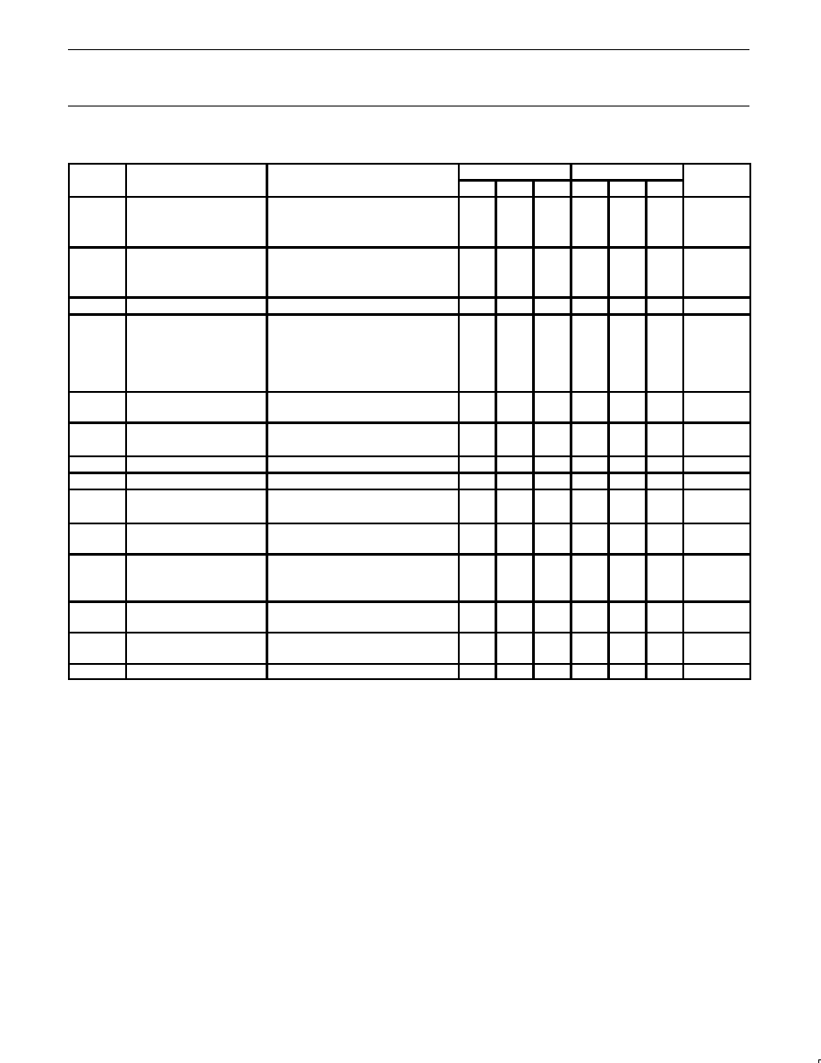
DC ELECTRICAL CHARACTERISTICS
1
SYMBOL
PARAMETER
TEST CONDITIONS
SE5537
NE5537
UNIT
SYMBOL
PARAMETER
TEST CONDITIONS
Min
Typ
Max
Min
Typ
Max
UNIT
T
J
=25
∞
C
1
3
2
7
mV
V
OS
Input offset voltage
4
Full temperature range
5
10
mV
T
J
=25
∞
C
5
25
10
50
nA
I
BIAS
Input bias current
4
Full temperature range
75
100
nA
Input impedance
T
J
=25
∞
C
10
10
10
10
Gain error
T
J
=25
∞
C
0.002
0.007
0.004
0.01
%
-10V
V
IN
10V, R
L
=2k
-11.5V
V
IN
11.5V,
R
L
=10k
Full temperature range
0.02
0.02
%
Feedthrough attenuation
ratio at 1kHz
T
J
=25
∞
C, C
H
=0.01
µ
F
86
96
80
90
dB
Output impedance
T
J
=25
∞
C, "HOLD" mode
0.5
2
0.5
4
Full temperature range
4
6
"HOLD" Step
2
T
J
=25
∞
C, C
H
=0.01
µ
F, V
OUT
=0
0.5
2.0
1.0
2.5
mV
I
CC
Supply current
4
T
J
=25
∞
C
4.5
6.5
4.5
7.5
mA
Logic and logic reference
input current
T
J
=25
∞
C
2
10
2
10
µ
A
Leakage current into hold
capacitor
4
T
J
=25
∞
C "hold" mode
3
6
50
6
100
pA
Acquisition time to 0.1%
V
OUT
=10V,
C
H
=1000pF
4
4
µ
s
C
H
=0.01
µ
F
20
20
µ
s
Hold capacitor charging
current
V
IN
-V
OUT
=2V
5
5
mA
SVRR
Supply voltage rejection
ratio
V
OUT
=0V
80
110
80
110
dB
Differential logic threshold
T
J
=25
∞
C
0.8
1.4
2.4
0.8
1.4
2.4
V
NOTES:
1. Unless otherwise specified, the following conditions apply: Unit is in "sample" mode. V
S
=
±
15V, T
J
=25
∞
C, -11.5V
V
IN
11.5V, C
H
=0.01
µ
F, and
R
L
=2k
. Logic reference voltage=0V and logic voltage=2.5V.
2. Hold step is sensitive to stray capacitive coupling between input logic signals and the hold capacitor. 1pF, for instance, will create an
additional 0.5mV step with a 5V logic swing and a 0.01F hold capacitor. Magnitude of the hold step is inversely proportional to hold capacitor
value.
3. Leakage current is measured at a junction temperature of 25
∞
C. The effects of junction temperature rise due to power dissipation or elevated
ambient can be calculated by doubling the 25
∞
C value for each 11
∞
C increase in chip temperature. Leakage is guaranteed over full input
signal range.
4. These parameters guaranteed over a supply voltage range of
±
5 to
±
18V.
Philips Semiconductors Linear Products
Product specification
NE/SE5537
Sample-and-hold amplifier
August 31, 1994
887
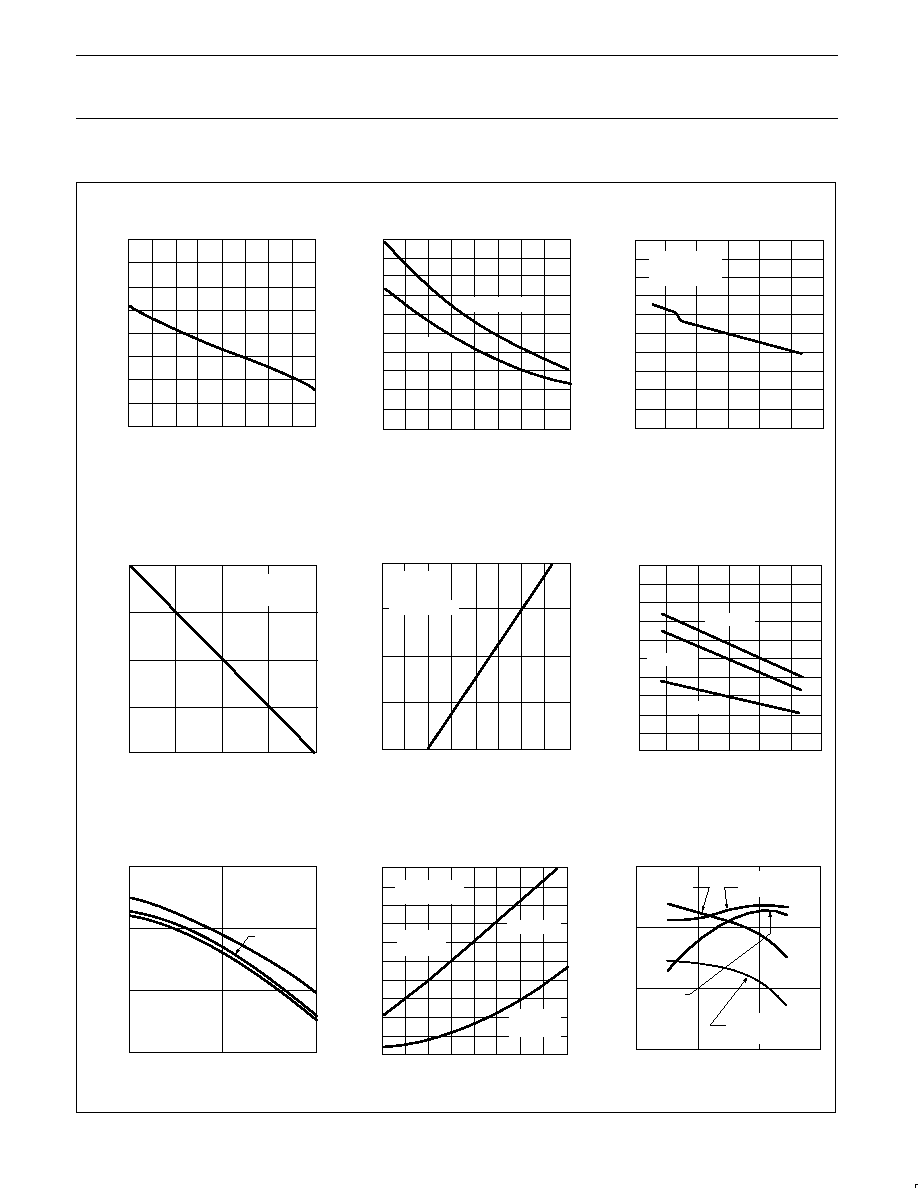
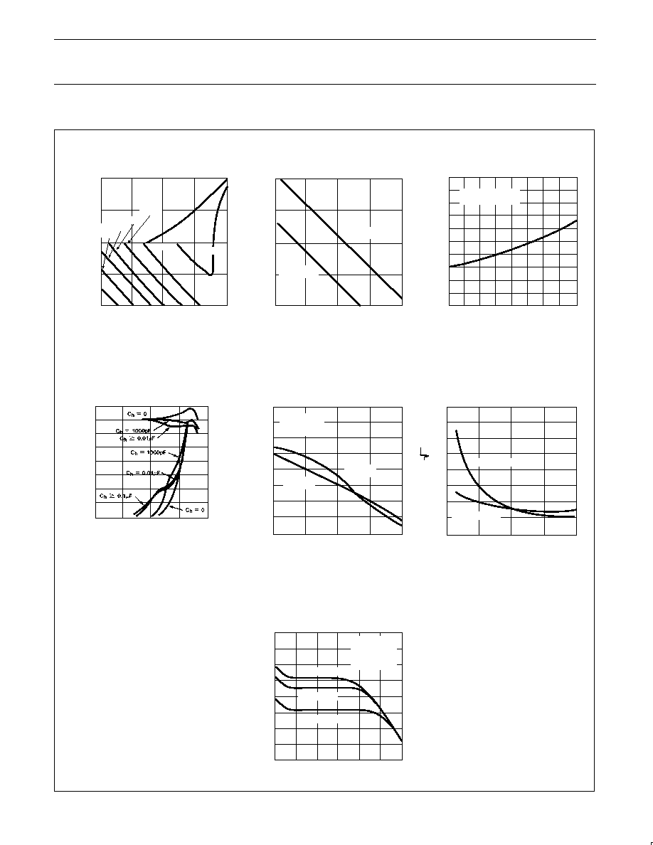
TYPICAL PERFORMANCE CHARACTERISTICS
Input Bias Current
Output Short-Circuit Current
Gain Error
Hold Step
Leakage Current Into
Hold Capacitor
Hold Step vs Input Voltage
Acquisition Time
Aperture Time
Capacitor Hysteresis
25
20
15
10
5
0
≠5
≠10
≠15
≠50
≠25
0
25
50
75
100
125
150
CURRENT (nA)
JUNCTION TEMPERATURE (
∞
C)
30
28
26
24
22
20
18
16
14
12
10
≠50
≠25
0
25
50
75
100
125
150
JUNCTION TEMPERATURE (
∞
C)
SOURCING
SINKING
CURRENT (mA)
100
10
1
0.1
0.01
100pF
1000pF
0.01
µ
F
0.1
µ
F
1
µ
F
HOLD STEP
(mV)
HOLD CAPACITOR
V+ = V≠ = 15V
TJ = 25
∞
C
10
VS =
±
15V
VOUT = 0
HOLD MODE
CURRENT (nA)
1
10≠1
10≠2
10≠3
JUNCTION TEMPERATURE (
∞
C)
≠50
≠25
0
25
50
75
100
125
150
TIME (ns)
2
1.8
1.6
1.4
1.2
1
0.8
0.6
0.4
0.2
0
≠15
≠10
≠5
0
5
10
15
NORMALIZED HOLD STEP
AMPLITUDE
INPUT VOLTAGE (V)
TJ = 100
∞
C
TJ = 25
∞
C
TJ = ≠55
∞
C
1
≠15
≠10
≠5
0
5
10
15
INPUT VOLTAGE (V)
INPUT
VOL
T
AGE -- OUTPUT
VOL
T
AGE (mV)
0.8
0.6
0.4
0.2
0
≠0.2
≠0.4
≠0.6
≠0.8
≠1
TJ = 25
∞
C
RL = 2k
SAMPLE MODE
1
10
100
1000
0.001
0.01
0.1
TJ = 25
∞
C
TIME ( s)
HOLD CAPACITOR (
µ
F)
VIN = 0 TO
±
10V
1%
0.1%
0.01%
µ
100
0.1
1
10
100
FINAL
SAG (mV)
SAMPLE TIME (ms)
10
1
0.1
MYLAR
TIME
CONSTANT
MYLAR
HYSTERESIS
POLYPROPYLENE
AND POLYSTYRENE
TIME CONSTANT
POLYPROPYLENE
AND POLYSTYRENE
HYSTERSIS
250
≠50
≠25
225
200
175
150
125
100
75
50
25
0
0
25
50
75
100 125
150
JUNCTION TEMPERATURE (
∞
C)
V+ = V≠ = 15V
VOUT
1mV
VIN ≠ 10V
NEGATIVE
INPUT
STEP
POSITIVE
INPUT
STEP
Philips Semiconductors Linear Products
Product specification
NE/SE5537
Sample-and-hold amplifier
August 31, 1994
888
TYPICAL PERFORMANCE CHARACTERISTICS
(Continued)
JUNCTION TEMPERATURE (
∞
C)
HOLD CAPACITOR
Dynamic Sampling Error
Output Droop Rate
Hold Settling Time
Phase and Gain
(Input-to-Output, Small-Signal)
Power Supply Rejection
Output Noise
Feedthrough Rejection
Ratio (Hold Mode)
100
10≠1
10≠2
10≠3
10≠4
100pF
1000pF
0.01
µ
F
0.1
µ
F
1
µ
F
TJ = 85
∞
C
TJ = 25
∞
C
V/ T (V/SEC)
2
1.8
1.6
1.4
1.2
1
0.8
0.6
0.4
0.2
0
≠50 ≠25
0
25
50
75 100 125 150
TIME ( S)
µ
V+ = V≠ = 15V
SETTLING TO 1mV
160
140
120
100
80
60
40
20
0
100
1k
10k
100k
1M
FREQUENCY (Hz)
REJECTION (dB)
NEGATIVE
SUPPLY
POSITIVE
SUPPLY
TJ = 25
∞
C
V+ = V≠ = 15V
VOUT = 0V
160
140
120
100
80
60
40
20
0
10
100
1k
10k
100k
FREQUENCY (Hz)
"HOLD" MODE
SAMPLE MODE
NOISE (nV/ Hz)
RA
TIO (dB)
FREQUENCY (Hz)
≠130
≠120
≠110
≠100
≠90
≠80
≠70
≠60
≠50
1
10
100
1k
10k
100k
1M
Ch = 0.1
µ
F
Ch = 0.01
µ
F
Ch = 1000pF
V+ = V≠ = 15V
VIN = 10VP-P
V7,8 = 0
TJ = 25
∞
C
ERROR (mV)
INPUT SLEW RATE (V/ms)
1k
10k
100k
1M
10M
80
70
60
50
40
30
20
10
0
100
10
≠10
≠100
±
1
0.1
1
10
100
1000
1000pF
3300pF
330pF
0.01
µ
F
0.033
µ
F
0.03
µ
F
0.1
µ
F
5
0
≠5
≠10
FREQUENCY (Hz)
GAIN--INPUT T
O OUTPUT (dB)
INPUT T
O OUTPUT PHASE DELA
Y
(DEG)

Philips Semiconductors Linear Products
Product specification
NE/SE5537
Sample-and-hold amplifier
August 31, 1994
889
SAMPLE-AND-HOLD
For many years designers have used the sample-and-hold (or
track-and-hold) to operate on analog information in a time frame
which is expedient.
By sampling a segment of the information and holding it until the
proper timing for converting to some form of control signal or
readout, the designer maintains certain freedom in performing
predetermined manipulative functions. Therefore, the
sample-and-hold can be defined as a "selective analog memory
cell".
The memory is volatile and will also decay with time.
When using the sample-and-hold method for evaluating signal
information, the designer is given the added feature of eliminating
outside noise elements. With the analog-to-digital converter
products available today, the "DC memory" of the sample-and-hold
can be easily converted to digital format and further incorporated
into microprocessor-based systems.
Parametric evaluation of the sample-and-hold will be discussed in
the following paragraphs.
DEFINITION OF TERMS
Acquisition Time --
The time required to acquire a new analog input voltage with an
output step of 10V. Note that acquisition time is not just the time
required for the output to settle, but also includes the time required
for all internal nodes to settle so that the output assumes the proper
value when switched to the hold mode.
Aperture Delay Time --
The time elapsed from the hold command to the opening of the
switch.
Aperture Jitter --
Also called "aperture uncertainty time", it is the time variation or
uncertainty with which the switch opens, or the time variation in
aperture delay.
Aperture Time --
The delay required between "HOLD" command and an input analog
transition, so that the transition does not affect the held output.
Bandwidth --
The frequency at which the gain is down 3dB from its DC value. It's
measured in sample (track) mode with a small-signal sine wave that
doesn't exceed the slew rate limit.
Dynamic Sampling Error --
The error introduced into the hold output due to a changing analog
input at the time the hold command is given. Error is expressed in
mV with a given hold capacitor value and input slew rate. Note that
this error term occurs even for long sample times.
Effective Aperture Delay --
The time difference between the hold command and the time at
which the input signal is at the held voltage.
Figure of Merit --
The ratio of the available charging current during sample mode to
the leakage current during hold mode.
Gain Error --
The ratio of output voltage swing to input voltage swing in the
sample mode expressed as a percent difference.
Hold Mode Droop --
The output voltage change per unit of time while in hold. Commonly
specified in V/s,
µ
V/
µ
s or other convenient units.
Hold Mode Feedthrough --
The percentage of an input sinusoidal signal that is measured at the
output of a sample-hold when it's in hold mode.
Hold Settling Time --
The time required for the output to settle within 1mV of final value
after the "HOLD" logic command.
Hold Step --
The voltage step at the output of the sample-and-hold when
switching from sample mode to hold mode with a steady (DC)
analog input voltage. Logic swing is 5V.
Sample-to-Hold Offset Error --
The difference in output voltage between the time the switch starts
to open, and the time when the output has settled completely. It is
caused by charge being transferred to the hold capacitor switch as it
opens.
Slew Rate --
The fastest rate at which the sample-and-hold output can change
(specified in V/
µ
s).
Threshold Level --
That level which causes the switch control to change state.
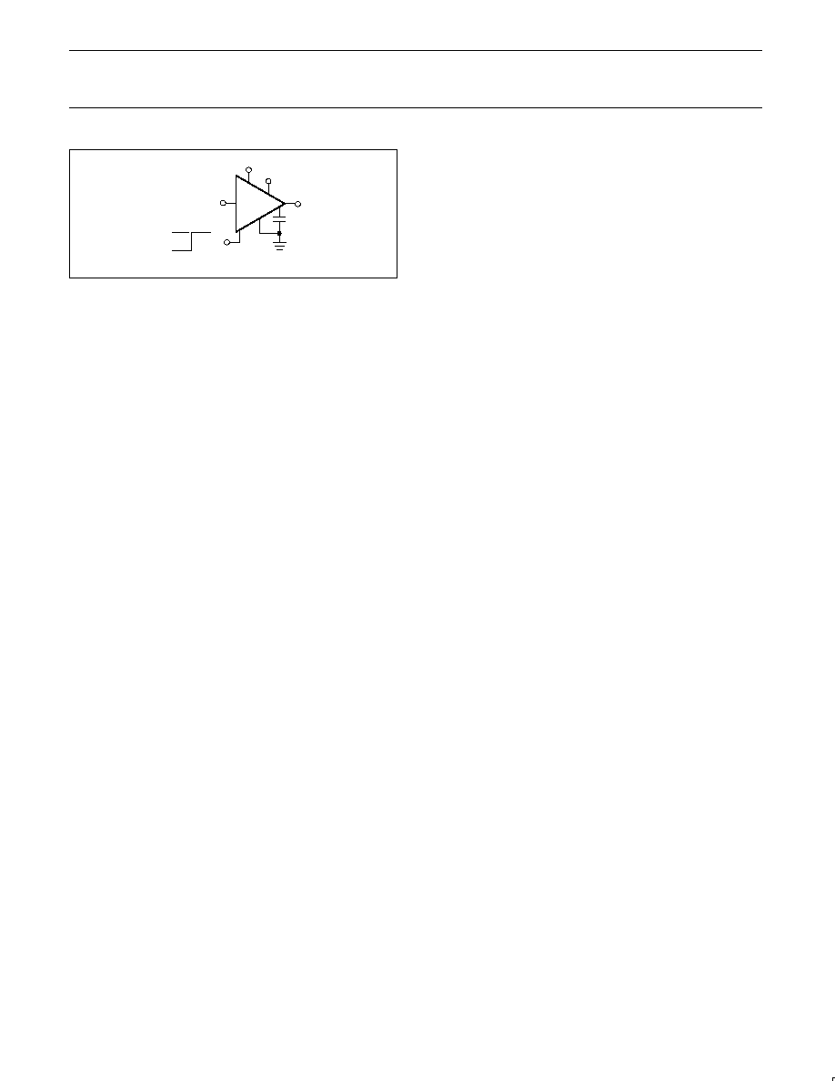
BASIC BLOCK DIAGRAM
The basic circuit concept of the sample-and-hold circuit incorporates
the use of two (2) operational amplifiers and a switch control
mechanism (which determines sample, hold or track conditions).
The block diagram of the NE5537 is a closed loop, non-inverting
unity gain sample-and-hold system. The input buffer amplifier
supplies the current necessary to charge the hold capacitor, while
the output buffer amplifier closes the loop so that the output voltage
is identical to the input voltage (with consideration for input offset
voltage, offset current, and temperature variations which are
common to all sample-and-hold circuits, be they monolithic, hybrid
or modular).
When the sampling switch is open (in the hold mode), the clamping
diodes close the loop around the input amplifier to keep it from being
overdriven into saturation.
The switch control is driven by external logic levels via a timing
sequence remote from the sample-and-hold device (See Figure 1).
The switch control has a floating reference (Pin 7), referred to as the
logic reference which makes the sample-and-hold device compatible
to several types of external logic signals (TTL, PMOS, and CMOS).
The switching device operates at a threshold level of 1.4V.
Philips Semiconductors Linear Products
Product specification
NE/SE5537
Sample-and-hold amplifier
August 31, 1994
890
Figure 1. Typical Connection
V+
V≠
OUTPUT
1
4
5
6
7
8
3
ANALOG INPUT
SAMPLE
HOLD
5V
0V
LOGIC
INPUT
Ch
The switch mechanism is on (sampling an information stream) when
the logic level is high (Pin 8 is 1.4V higher than Pin 7) and presents
a load of 5
µ
A to the input logic signal. The analog sampled signal is
amplified, stored (in the external holding capacitor), and buffered. At
the end of the sampling period, the internal switch mechanism turns
off (switch opens) and the "stored analog memory" information on
the external capacitor (Pin 6) is loaded down by an operational
amplifier connected in the unity gain non-inverting configuration.
This input impedance of this amplifier is effectively:
R
= R
IN
(A
OL
) / (1 + 1/A)
where
R
= Effective input impedance
R
IN
= Open-loop input impedance
A
OL
= Open-loop gain
A
= AC loop gain
Therefore, the higher the open-loop gain of the second operational
amplifier, the larger the effective loading on the capacitor. The larger
the load, the lower the "leakage" current and the better the droop
characteristics.
In actuality, the amplifiers are designed with special leakage current
cancellation circuits along with FET input devices. The leakage
current cancellation circuits give better high temperature operation.
(Remember that the FET amplifiers double in required bias current
for every 10 degree increase in junction temperature.)
Sampling time for the NE5537 is less than 10
µ
s (measured to 0.1%
of input signal). Leakage current is 6pA at a rate output load of 2k
.
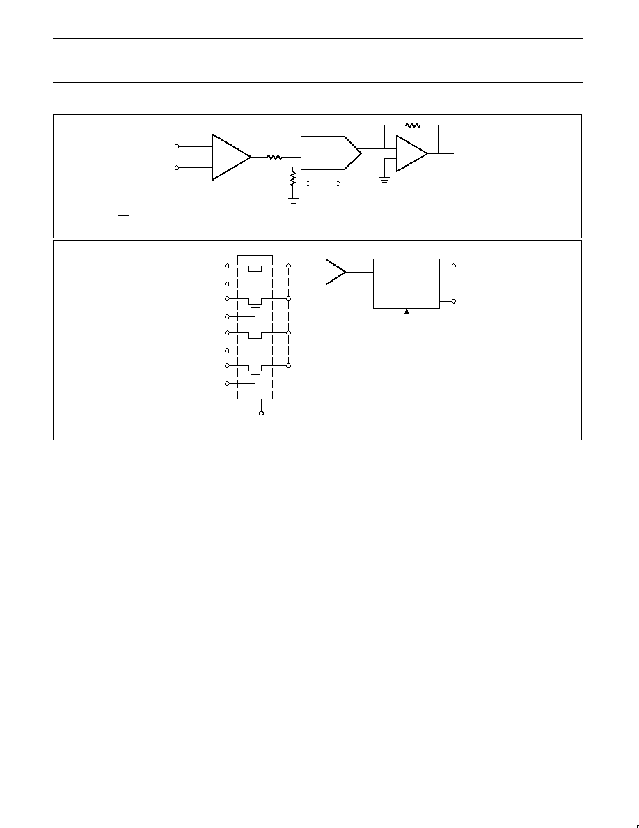
BASIC APPLICATIONS
Multiplying DAC
As depicted in the block diagram of Figure 2, the sample-and-hold
circuit is used to supply a "variable" reference to the digital-to-analog
converter. As the input reference varies, the output will change in
accordance with Equation 1, shown in Figure 2.
Varying the input signal reference level can aid the system in
performing both compression and expansion operations. The
multiplying DACs used are the Philips Semiconductors NE/SE5008;
however, if the rate of change of the reference variation is kept slow
enough, a microprocessor-compatible DAC can be incorporated,
such as the NE5018 or the NE5020.
DATA ACQUISITION SYSTEMS
As mentioned earlier, the designer may wish to operate on several
different segments of an "analog" signal; however, he is limited by
the fact that only one analog-to-digital converter channel is available
to him. Figure 3 shows the means by which a multiplexing system
may be accomplished.
APPLICATION HINTS
Hold Capacitor
A significant source of error in an accurate sample-and-hold circuit
is dielectric absorption in the hold capacitor. A mylar cap, for
instance, may "sag back" up to 0.2% after a quick change in voltage.
A long "soak" time is required before the circuit can be put back in
the hold mode with this type of capacitor. Dielectrics with very low
hysteresis are polystyrene, polypropylene, and teflon. Other types
such as mica and polycarbonate are not nearly as good. Ceramic is
unusable with >1% hysteresis. The advantage of polypropylene over
polystyrene is that it extends the maximum ambient temperature
from 85
∞
C to 100
∞
C. The hysteresis relaxation time constant in
polystyrene, for instance, is 10-50ms. If A-to-D conversion can be
made within 1ms, hysteresis error will be reduced by a factor of ten.
DC ZEROING
DC zeroing is accomplished by connecting the offset adjust pin to
the wiper of a 1k
potentiometer which has one end tied to V+ and
the other end tied through a resistor to ground. The resistor should
be selected to give 0.6mA through the 1k
potentiometer.
Sampling Dynamic Signals
Sampling errors due to moving (changing) input signals are of
significant concern to designers employing sample-and-hold circuits.
There exist finite phase delays through the sample-and-hold circuit
causing an input-output phase of differential for moving signals. In
addition, the series protection resistor (300
to Pin 6 of the NE5537)
will add an RC time constant, over and above the slew rate limitation
of the input buffer/current drive amplifier. This means that at the
moment the "HOLD" command arrives, the hold capacitor voltage
may be somewhat different from the actual analog input. The effect
of these delays is opposite to the effect created by delays in the
logic which switches the circuit from sample to hold. For example,
consider an analog input of 20 V
P-P
at 10kHz. Maximum dV/dt is
0.6V/
µ
s. With no analog phase delay and 100ns logic delay, one
could expect up to (0.1
µ
s) (0.6V/
µ
s) =60mV error if the "HOLD"
signal arrived near maximum dV/dt of the input. A positive-going
input would give a
±
60mV error. Now assume a 1MHz (3dB)
bandwidth for the overall analog loop. This generates a phase delay
of 160ns. If the hold capacitor sees this exact delay, then error due
to analog delay will be (0.16
µ
s) (0.6V/
µ
s)=-96mV (analog) for a total
of -36mV. To add to the confusion, analog delay is proportional to
hold capacitor value, while digital delay remains constant. A family
of curves (dynamic sampling error) is included to help estimate
errors.
Philips Semiconductors Linear Products
Product specification
NE/SE5537
Sample-and-hold amplifier
August 31, 1994
891
VOUT
Figure 2. Multiplying DAC Application
VIN
+VREFIN
NE5537
5k
5008/DAC-08
530
5k
D0-D7
NOTE:
V
OUT
+
V
IN
x
1
256
(20 D
0
)
21D
1
)
27D
7
) Equation 1
Figure 3. Analog Data Multiplexing
SD5000
NE5537
A/D
CONVERTER
ANALOG INPUT 1
CONTROL 1
ANALOG INPUT 2
CONTROL 2
ANALOG INPUT 3
CONTROL 3
ANALOG INPUT 4
CONTROL 4
SUCCESSIVE APPROXIMATION
(NE5034, NE5037)
or INTEGRATING TYPE ADC
SUBSTRATE
D0
D7
A curve labeled "Aperture Time" has been included for sampling
conditions where the input is steady during the sampling period, but
may experience a sudden change nearly coincident with the "HOLD"
command. This curve is based on a 1mV error fed into the output.
A second curve, "Hold Settling Time," indicates the time required for
the output to settle to 1mV after the "HOLD" command.
Digital Feedthrough
Fast rise time logic signals can cause hold errors by feeding
externally into the analog input at the same time the amplifier is put
into the hold mode. To minimize this problem, board layout should
keep logic lines as far as possible from the analog input. Grounded
guarding traces may also be used around the input line, especially if
it is driven from a high impedance source. Reducing high amplitude
logic signals to 2.5V will also help.
Logic signals also couple to the hold capacitor. This hold capacitor
should be guarded by a PC card trace connected to the
sample-and-hold output. This will also minimize board leakage.
SPECIAL NOTES
1. Not all definitions herein defined are measured parametrically for
the NE5537, but are legitimate terms used in sample-and-hold
systems.
2. Reference should be made to Design Engineering, Volumes 23
(Nov. 8, 1978), 25 (Dec. 6, 1978) and 26 (Dec. 20, 1978) for
articles written by Eugene Zuch of Datel Systems, Inc., for a
further discussion of sample-and-hold circuits.
3. Reference also made to National Semiconductor Corporation's
Special Functions Data Book (1976).