
Philips
Semiconductors
NE56631-XX
Active-LOW system reset
Product data
Supersedes data of 2002 Oct 07
2003 Feb 14
INTEGRATED CIRCUITS

Philips Semiconductors
Product data
NE56631-XX
Active-LOW system reset
2
2003 Feb 14
GENERAL DESCRIPTION
The NE56631-XX is a family of Active-LOW, power-on resets that
offers precision threshold voltage detection within
±
3% and super
low operating supply current of typically 1.5
µ
A.
Several detection threshold voltages are available at 1.9 V, 2.0 V,
2.7 V, 2.8 V, 2.9 V, 3.0 V, 3.1 V, 4.2 V, 4.3 V, 4.4 V, 4.5 V, and 4.6 V.
Other thresholds are offered upon request at 100 mV steps from
1.9 V to 4.6 V.
With its ultra low supply current and high precision voltage threshold
detection capability, the NE56631-XX is well suited for various
battery powered applications such as reset circuits for logic and
microprocessors, voltage check, and level detecting.
FEATURES
∑
High precision threshold detection voltage:
V
S
±
3%
∑
Super low operating supply current:
I
CCH
=1.5
µ
A typ.;
I
CCL
=1.0
µ
A typ.
∑
Hysteresis voltage:
50 mV typ.
∑
Internal Power-On-Reset Delay time:
20
µ
s typ.
∑
Detection threshold voltage:
1.9 V, 2.0 V, 2.7 V, 2.8 V, 2.9 V,
3.0 V, 3.1 V, 4.2 V, 4.3 V, 4.4 V, 4.5 V, and 4.6 V
∑
Other detection threshold voltages available upon request at
100 mV steps from 1.9 V to 4.6 V
∑
Large low reset output current:
30 mA typ.
∑
Reset assertion with V
CC
down to 0.65 V typ.
APPLICATIONS
∑
Reset for microprocessor and logic circuits
∑
Voltage level detection circuit
∑
Battery voltage check circuit
∑
Detection circuit for battery backup
SIMPLIFIED SYSTEM DIAGRAM
NE56631-XX
V
CC
RESET
V
CC
GND
V
OUT
LOGIC SYSTEM
SL01739
Figure 1. Simplified system diagram.
Philips Semiconductors
Product data
NE56631-XX
Active-LOW system reset
2003 Feb 14
3
ORDERING INFORMATION
TYPE NUMBER
PACKAGE
TEMPERATURE
TYPE NUMBER
NAME
DESCRIPTION
RANGE
NE56631-XXD
SOT23-5 / SOT25 (SO5)
plastic small outline package; 5 leads (see dimensional drawing)
≠20 to +75
∞
C
NOTE:
The device has 12 voltage output options, indicated by the XX on
the `Type number'.
XX
VOLTAGE (Typical)
19
1.9 V
20
2.0 V
27
2.7 V
28
2.8 V
29
2.9 V
30
3.0 V
31
3.1 V
42
4.2 V
43
4.3 V
44
4.4 V
45
4.5 V
46
4.6 V
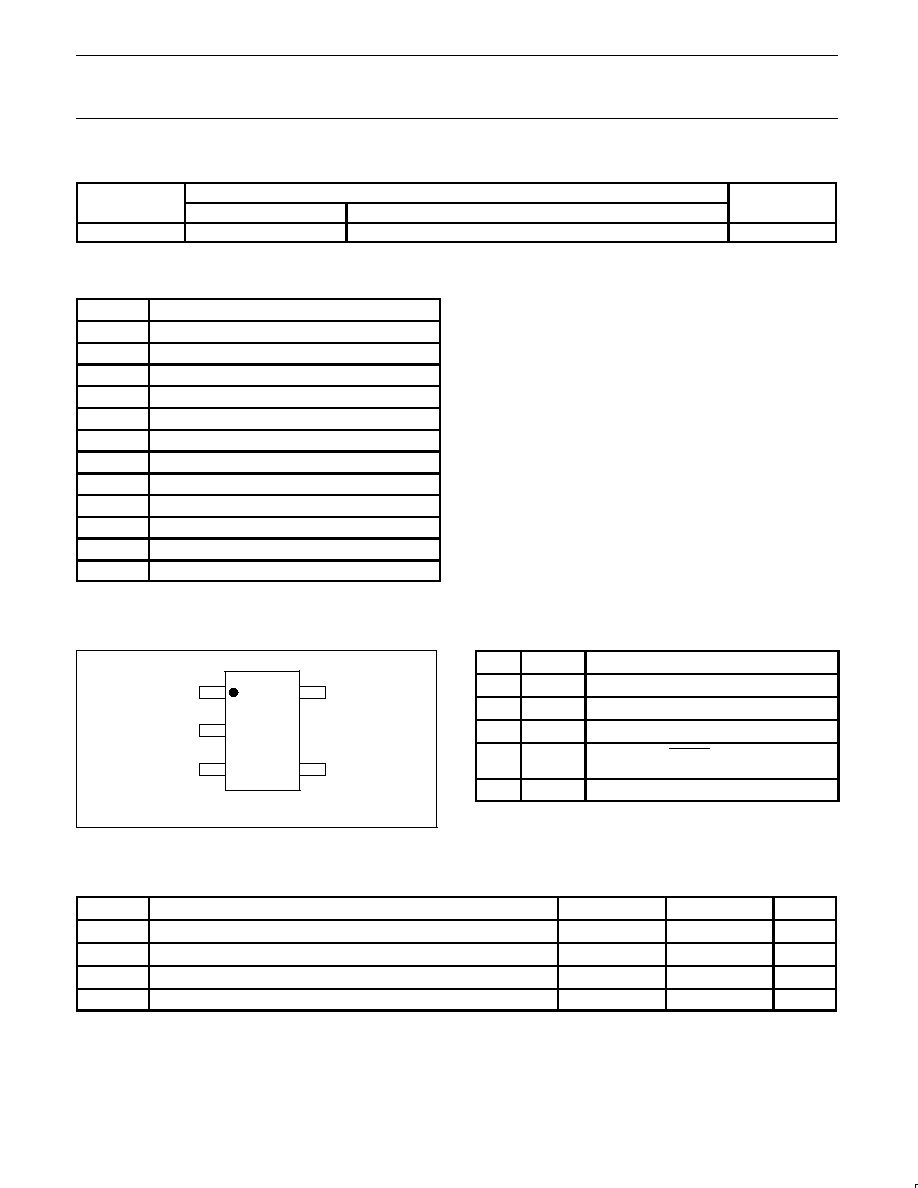
PIN CONFIGURATION
SL01737
1
2
3
4
5
V
CC
V
OUT
GND
SUB
NC
NE56631-XX
Figure 2. Pin configuration.
PIN DESCRIPTION
PIN
SYMBOL
DESCRIPTION
1
NC
No connection.
2
SUB
Substrate. Connect to ground (GND).
3
GND
Ground. Negative supply.
4
V
OUT
Reset output (RESET).
Active-LOW, open collector.
5
V
CC
Positive supply voltage
MAXIMUM RATINGS
SYMBOL
PARAMETER
MIN.
MAX.
UNIT
V
CC
Supply voltage
≠0.3
+10
V
T
amb
Ambient operating temperature
≠20
+75
∞
C
T
stg
Storage temperature
≠40
+125
∞
C
P
D
Power dissipation
≠
150
mW

Philips Semiconductors
Product data
NE56631-XX
Active-LOW system reset
2003 Feb 14
4
ELECTRICAL CHARACTERISTICS
T
amb
= 25
∞
C, unless otherwise specified.
SYMBOL
PARAMETER
CONDITIONS
MIN.
TYP.
MAX.
UNIT
V
S
Detection threshold voltage
R
L
= 470
; V
OL
0.4 V;
V
CC
= HIGH-to-LOW
0.97 V
S
V
S
1.03 V
S
V
V
S
Hysteresis voltage
R
L
= 470
;
V
CC
= LOW-to-HIGH-to-LOW
30
50
100
mV
V
S
/
T
Detection threshold voltage
temperature coefficient
R
L
= 470
; T
amb
= ≠20
∞
C to +75
∞
C
≠
±
0.01
≠
%/
∞
C
V
OL
LOW-level output voltage
V
CC
= V
S(min)
≠ 0.05 V; R
L
= 470
≠
0.2
0.4
V
I
LO
Output leakage current
V
CC
= 10 V; V
O
= V
CC
≠
≠
±
0.1
V
I
CCL
Supply current (LOW Reset)
V
CC
= V
S(min)
≠ 0.05 V; R
L
=
≠
1.0
2.0
µ
A
I
CCH
Supply current (HIGH Reset)
V
CC
= V
S(typ)
/ 0.85 V; R
L
=
≠
1.5
2.5
µ
A
t
PLH
HIGH-to-LOW delay time
C
L
= 100 pF; R
L
= 4.7 k
≠
20
60
µ
s
t
PHL
LOW≠to-HIGH delay time
C
L
= 100 pF; R
L
= 4.7 k
≠
20
60
µ
s
V
OPL
Minimum operating threshold voltage
R
L
= 4.7 k
; V
OL
0.4 V
≠
0.65
0.80
V
I
OL1
Output current (LOW Reset) 1
V
O
= 0.4 V; R
L
= 0;
V
CC
= V
S(min)
≠ 0.05 V
≠
30
≠
mA
I
OL2
Output current (LOW Reset) 2
V
O
= 0.4 V; R
L
= 0;
V
CC
= V
S(min)
≠ 0.15 V;
T
amb
= ≠30
∞
C to +80
∞
C
≠
23
≠
mA

Philips Semiconductors
Product data
NE56631-XX
Active-LOW system reset
2003 Feb 14
5
TYPICAL PERFORMANCE CURVES
SL01845
AMBIENT TEMPERATURE, T
amb
(
∞
C)
≠25
0
25
50
75
4.60
4.55
4.50
4.45
4.40
DETECTION
VOL
T
AGE, V (mV)
S
R
L
= 470
V
OL
0.4 V
V
CC
= HIGH-to-LOW
Figure 3. Detection voltage versus ambient temperature.
SL01841
AMBIENT TEMPERATURE, T
amb
(
∞
C)
≠25
0
25
50
75
31
30
29
28
OUTPUT
CURRENT
(RESET
LOW), I (mA)
32
33
34
OL
V
O
= 0.4 V
R
L
= 0
V
CC
= V
S(min)
≠ 0.05 V
Figure 4. Detection voltage versus ambient temperature.
SL01840
AMBIENT TEMPERATURE, T
amb
(
∞
C)
≠25
0
25
50
75
1.7
1.6
1.5
1.4
1.3
1.8
SUPPL
Y
CURRENT
(RESET
LOW), I (
A)
µ
CCL
V
CC
= V
S(min)
≠ 0.05 V
R
L
=
Figure 5. Supply current (Reset LOW) versus
ambient temperature.
HYSTERESIS
VOL
T
AGE, V (mV)
SL01842
AMBIENT TEMPERATURE, T
amb
(
∞
C)
≠25
0
25
50
75
80
70
60
50
40
30
20
S
R
L
= 470
V
CC
= LOW-to-HIGH-to-LOW
Figure 6. Hysteresis voltage versus ambient temperature.
MINIMUM OPERA
TING
THRESHOLD
VOL
T
AGE,
SL01844
AMBIENT TEMPERATURE, T
amb
(
∞
C)
≠25
0
25
50
75
0.9
0.8
0.7
0.6
0.5
0.4
R
L
= 4.7 k
V
OL
0.4 V
V (V)
OPL
Figure 7. Minimum operating threshold voltage versus
ambient temperature.
SL01843
AMBIENT TEMPERATURE, T
amb
(
∞
C)
≠25
0
25
50
75
190
170
150
130
110
LOW
-LEVEL
OUTPUT
VOL
T
AGE, V (V)
OL
V
CC
= V
S(min)
≠ 0.05 V
R
L
= 470
Figure 8. LOW-level output voltage versus
ambient temperature.
Philips Semiconductors
Product data
NE56631-XX
Active-LOW system reset
2003 Feb 14
6
TECHNICAL DISCUSSION
The NE56631-XX is a Bipolar IC designed to provide power source
monitoring and a system reset function in the event the power sags
below an acceptable level for the system to operate reliably. The IC
is designed to generate a reset signal for a wide range of
microprocessor and other logic systems. The NE56631-XX can
operate at supply voltage up to 10 volts. The series includes several
devices with precision threshold reset voltage values of 1.9, 2.0, 2.7,
2.8, 2.9, 3.0, 3.1, 4.2, 4.3, 4.4, 4.5, 4.6 V. The reset threshold
incorporates a typical hysteresis of 50 mV to prevent erratic
reasserts from being generated. An internal fixed delay time circuit
provides a fixed power-on-reset delay of typically 20
µ
s with a
guaranteed maximum delay of 60
µ
s.
The output of the NE56631-XX utilizes an open collector topology,
which requires an external pull-up resistor to V
CC
. Though this may
be regarded as a disadvantage, it is advantageous in many
sensitive applications. Since the open collector output cannot source
reset current when both are operated from a common supply, the
NE56631-XX offers a safe interconnect to a wide variety of
microprocessors.
The NE56631-XX operates at low supply currents, typically 1.5
µ
A,
while offering high precision of the threshold detection (
±
3%).
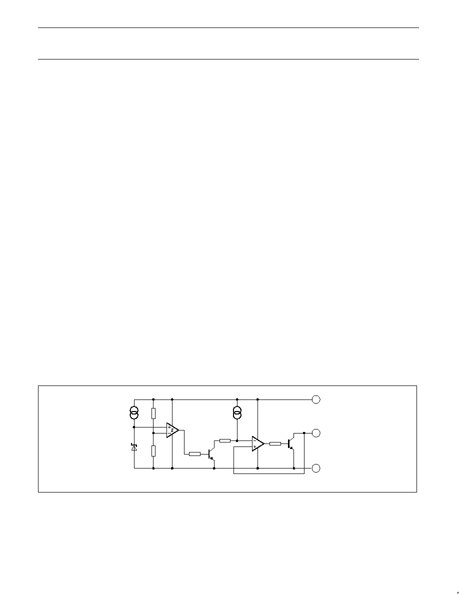
Figure 9 is a functional block diagram of the NE56631-XX. The
internal reference source voltage is typically 0.65 V over the
temperature range. The reference voltage is connected to the
non-inverting input of the threshold comparator while the inverting
input monitors the supply voltage through a voltage divider network
made up of R1 and R2. The output of the comparator drives the
series base resistor, R3 of a common emitter amplifier, Q1. The
collector of Q1 is connected through R4 to the inverting terminal of
the op amp. The op amp output is connected to the series base
resistor, R5 of the output common emitter transistor, Q2. The
collector output of Q2 is connected to the non-inverting terminal of
the op amp which drives it.
When the supply voltage sags to the threshold detection voltage, the
resistor divider network supplies a voltage to the inverting terminal of
the threshold comparator which is less than V
REF
, causing the
output of the comparator to go to a HIGH state. This causes the
common emitter amplifier, Q1 to turn on pulling down the
non-inverting terminal of the op amp, which causes its output to go
to a HIGH state. This high output level turns on the output common
emitter transistor, Q2. The collector output of Q2 is pulled LOW
through the external pull-up resistor, thereby asserting the
Active-LOW reset.
The bipolar common emitter transistor, Q1and the op amp
establishes threshold hysteresis by turning on when the threshold
comparator goes to a HIGH state (when V
CC
sags to or below the
threshold level). With the output of Q2 connected to the
non-inverting terminal of the op amp, the non-inverting terminal of
the op amp has a level near ground at about 0.4 V when the reset is
asserted (Active-LOW). For the op amp to reverse its output, the
comparator output and Q1 must overcome the additional pull-down
voltage present on the op amp inverting input. The differential
voltage required to do this establishes the hysteresis voltage of the
sensed threshold voltage. Typically it is 50 mV.
When V
CC
voltage sags, and it is below the detection Threshold
(V
SL
), the device will assert a Reset LOW output at or near ground
potential. As V
CC
voltage rises from (V
CC
< V
SL
) to V
SH
or higher,
the Reset is released and the output follows V
CC
. Conversely,
decreases in V
CC
from (V
CC
> V
SL
) to V
SL
will cause the output to
be pulled to ground.
Hysteresis Voltage = Released Voltage ≠ Detection Threshold
Voltage
V
S
= V
SH
≠ V
SL
where:
V
SH
= V
SL
+
V
S
V
SL
= V
SH
≠
V
S
When V
CC
drops below the minimum operating voltage, typically
0.65 V, the output is undefined and the output reset low assertion is
not guaranteed. At this level of V
CC
the output will try to rise to V
CC
.
3
4
R3
Q1
Q2
R5
V
OUT
GND
OP1
CO1
R2
R1
5
V
REF
V
CC
SL01738
R4
Figure 9. Functional diagram.

Philips Semiconductors
Product data
NE56631-XX
Active-LOW system reset
2003 Feb 14
7
TIMING DIAGRAM
The Timing Diagram in Figure 10 depicts the operation of the device.
Letters A≠J on the Time axis indicates specific events.
A:
At "A", V
CC
begins to increase. Also the V
OUT
voltage initially
increases but abruptly decreases when V
CC
reaches the level
(approximately 0.65 V) that activates the internal bias circuitry and
RESET is asserted.
B:
At "B", V
CC
reaches the threshold level of V
SH
. At this point the
device releases the hold on the V
OUT
reset. The Reset output V
OUT
tracks V
CC
as it rises above V
SH
(assuming the reset pull-up resistor
R
PU
is connected to V
CC
). In a microprocessor-based system these
events release the reset from the microprocessor, allowing the
microprocessor to function normally.
C-D:
At "C", V
CC
begins to fall, causing V
OUT
to follow. V
CC
continues to fall until the V
SL
undervoltage detection threshold is
reached at "D". This causes a reset signal to be generated (V
OUT
RESET goes LOW).
D-E:
Between "D" and "E", V
CC
starts rising.
E:
At "E", V
CC
rises to the V
SH
level. Once again, the device
releases the hold on the V
OUT
reset. The Reset output tracks V
CC
as it rises above V
SH
.
F-G:
At "F", V
CC
is above the upper threshold and begins to fall,
causing V
OUT
to follow it. As long as V
CC
remains above the V
SH
,
no reset signal will be triggered. Before V
CC
falls to the V
SH
, it
begins to rise, causing V
OUT
to follow it. At "G", V
CC
returns to
normal.
H:
At event "H", V
CC
falls until the V
SL
undervoltage detection
threshold is reached. At this level, a RESET signal is generated and
V
OUT
goes LOW.
J:
At "J", the V
CC
voltage has decreased until normal internal
circuit bias is unable to maintain a V
OUT
reset. As a result, V
CC
may
rise to less than 0.65 V. As V
CC
decreases further, the V
OUT
reset
also decreases to zero.
SL01740
V
CC
V
OUT
TIME
V
SH
V
SL
0
0
A
B
C
G
H
J
D
E
F
V
S
Figure 10. Timing diagram.
Philips Semiconductors
Product data
NE56631-XX
Active-LOW system reset
2003 Feb 14
8
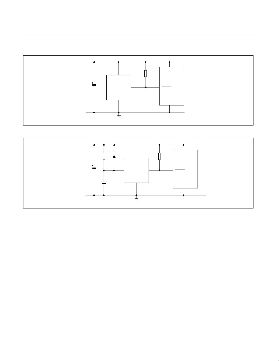
APPLICATION INFORMATION
RESET
V
CC
SUPPLY
GND
V
CC
NE56631-XX
V
SS
V
OUT
R
PU
CPU
SL01741
Figure 11. Conventional reset application for NE56631-XX.
RESET
V
CC
SUPPLY
GND
V
CC
NE56631-XX
V
SS
V
OUT
R
PU
CPU
SL01742
R
D
Figure 12. Power On Reset circuit for NE56631-XX.
The Power ON Reset Circuit shown in Figure 12 is an example of
obtaining a stable reset condition upon power-up. If power supply
rises abruptly, the RESET may go "HIGH" momentarily when V
CC
is
below the minimum operating voltage (0.85 V). To overcome this
undesirable response, a resistor in placed between positive supply,
V
CC
and V
CC
pin and a capacitor from V
CC
pin to ground. The RC
circuit solution works reasonably well for power-up as long as the
power supply voltage rises faster than the RC time constant. The
RC network provides the necessary reset delay to hold the
microprocessor in reset until its circuitry settles down and normal
operation begins. When the supply turns off, the diode provides a
path for the capacitor to discharge to more quickly assert logic LOW
reset.

Philips Semiconductors
Product data
NE56631-XX
Active-LOW system reset
2003 Feb 14
9
PACKING METHOD
The NE56631-XX is packed in reels, as shown in Figure 13.
SL01305
TAPE DETAIL
COVER TAPE
CARRIER TAPE
REEL
ASSEMBLY
TAPE
GUARD
BAND
BARCODE
LABEL
BOX
Figure 13. Tape and reel packing method.
Philips Semiconductors
Product data
NE56631-XX
Active-LOW system reset
2003 Feb 14
10
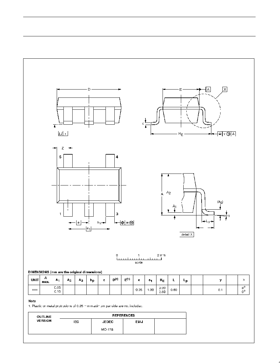
SOT23-5: plastic small outline package; 5 leads; body width 1.5 mm
1.35
1.2
1.0
0.025
0.55
0.41
0.22
0.08
3.00
2.70
1.70
1.50
0.55
0.35

Philips Semiconductors
Product data
NE56631-XX
Active-LOW system reset
2003 Feb 14
11
REVISION HISTORY
Rev
Date
Description
_2
20030214
Product data (9397 750 11131); ECN 853-2328 29155 of 06 November 2002.
Supersedes data of 2002 Oct 07 (9397 750 10266).
Modifications:
∑
Page 6, Technical discussion; third paragraph: from "... typically 1.5 mA, ..." to "... typically 1.5
µ
A, ..."
_1
20021007
Product data (9397 750 10266); ECN 853≠2328 27919 of 25 March 2002.
Definitions
Short-form specification -- The data in a short-form specification is extracted from a full data sheet with the same type number and title. For detailed information see
the relevant data sheet or data handbook.
Limiting values definition -- Limiting values given are in accordance with the Absolute Maximum Rating System (IEC 60134). Stress above one or more of the limiting
values may cause permanent damage to the device. These are stress ratings only and operation of the device at these or at any other conditions above those given
in the Characteristics sections of the specification is not implied. Exposure to limiting values for extended periods may affect device reliability.
Application information -- Applications that are described herein for any of these products are for illustrative purposes only. Philips Semiconductors make no
representation or warranty that such applications will be suitable for the specified use without further testing or modification.
Disclaimers
Life support -- These products are not designed for use in life support appliances, devices, or systems where malfunction of these products can reasonably be
expected to result in personal injury. Philips Semiconductors customers using or selling these products for use in such applications do so at their own risk and agree
to fully indemnify Philips Semiconductors for any damages resulting from such application.
Right to make changes -- Philips Semiconductors reserves the right to make changes in the products--including circuits, standard cells, and/or software--described
or contained herein in order to improve design and/or performance. When the product is in full production (status `Production'), relevant changes will be communicated
via a Customer Product/Process Change Notification (CPCN). Philips Semiconductors assumes no responsibility or liability for the use of any of these products, conveys
no license or title under any patent, copyright, or mask work right to these products, and makes no representations or warranties that these products are free from patent,
copyright, or mask work right infringement, unless otherwise specified.
Contact information
For additional information please visit
http://www.semiconductors.philips.com.
Fax: +31 40 27 24825
For sales offices addresses send e-mail to:
sales.addresses@www.semiconductors.philips.com.
©
Koninklijke Philips Electronics N.V. 2003
All rights reserved. Printed in U.S.A.
Date of release: 02-03
Document order number:
9397 750 11131
Philips
Semiconductors
Data sheet status
[1]
Objective data
Preliminary data
Product data
Product
status
[2] [3]
Development
Qualification
Production
Definitions
This data sheet contains data from the objective specification for product development.
Philips Semiconductors reserves the right to change the specification in any manner without notice.
This data sheet contains data from the preliminary specification. Supplementary data will be published
at a later date. Philips Semiconductors reserves the right to change the specification without notice, in
order to improve the design and supply the best possible product.
This data sheet contains data from the product specification. Philips Semiconductors reserves the
right to make changes at any time in order to improve the design, manufacturing and supply. Relevant
changes will be communicated via a Customer Product/Process Change Notification (CPCN).
Data sheet status
[1] Please consult the most recently issued data sheet before initiating or completing a design.
[2] The product status of the device(s) described in this data sheet may have changed since this data sheet was published. The latest information is available on the Internet at URL
http://www.semiconductors.philips.com.
[3] For data sheets describing multiple type numbers, the highest-level product status determines the data sheet status.
Level
I
II
III