Philips Semiconductors Linear Products
Product specification
NE/SE566
Function generator
398
April 15, 1992
853-0910 06454
DESCRIPTION
The NE/SE566 Function Generator is a voltage-controlled oscillator
of exceptional linearity with buffered square wave and triangle wave
outputs. The frequency of oscillation is determined by an external
resistor and capacitor and the voltage applied to the control terminal.
The oscillator can be programmed over a ten-to-one frequency
range by proper selection of an external resistance and modulated
over a ten-to-one range by the control voltage, with exceptional
linearity.
FEATURES
∑
Wide range of operating voltage (up to 24V; single or dual)
∑
High linearity of modulation
∑
Highly stable center frequency (200ppm/
∞
C typical)
∑
Highly linear triangle wave output
∑
Frequency programming by means of a resistor or capacitor,
voltage or current
∑
Frequency adjustable over 10-to-1 range with same capacitor
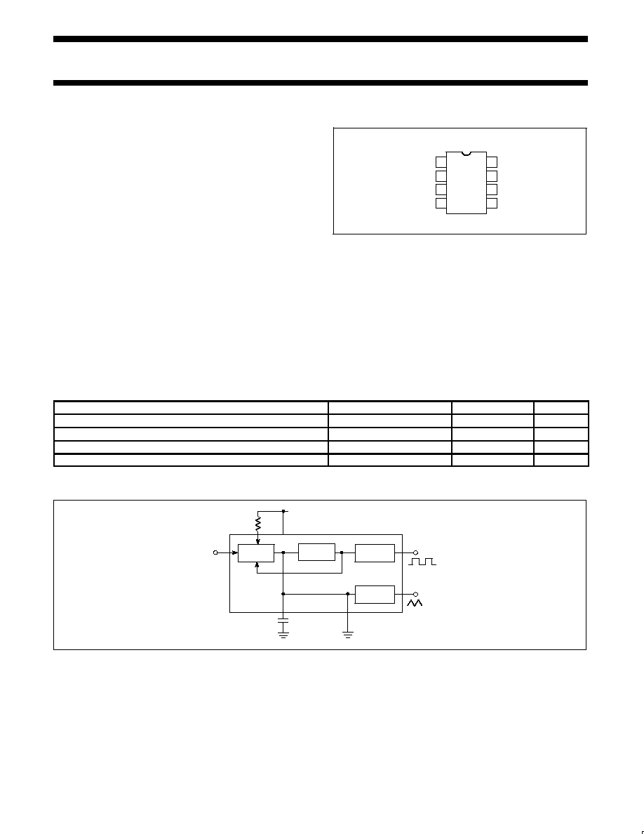
PIN CONFIGURATIONS
D, N Packages
1
2
3
4
5
6
7
8
GROUND
NC
SQUARE WAVE OUTPUT
TRIANGLE WAVE OUTPUT
V+
MODULATION INPUT
C1
R1
TOP VIEW
APPLICATIONS
∑
Tone generators
∑
Frequency shift keying
∑
FM modulators
∑
Clock generators
∑
Signal generators
∑
Function generators
ORDERING INFORMATION
DESCRIPTION
TEMPERATURE RANGE
ORDER CODE
DWG #
8-Pin Plastic Small Outline (SO) Package
0 to +70
∞
C
NE566D
0174C
14-Pin Ceramic Dual In-Line Package (CERDIP)
0 to +70
∞
C
NE566F
0581B
8-Pin Plastic Dual In-Line Package (DIP)
0 to +70
∞
C
NE566N
0404B
8-Pin Plastic Dual In-Line Package (DIP)
-55
∞
C to +125
∞
C
SE566N
0404B
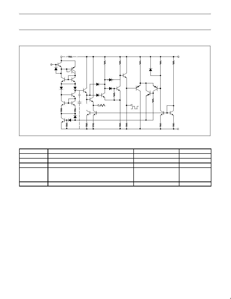
BLOCK DIAGRAM
VC
MODULATION
INPUT
R1
V+
6
8
5
7
C1
SCHMITT
TRIGGER
BUFFER
AMPLIFIER
BUFFER
AMPLIFIER
3
4
CURRENT
SOURCES
Philips Semiconductors Linear Products
Product specification
NE/SE566
Function generator
April 15, 1992
400
DC ELECTRICAL CHARACTERISTICS
T
A
=25
∞
C, V
CC
=
±
6V, unless otherwise specified.
SYMBOL
PARAMETER
SE566
NE566
UNIT
SYMBOL
PARAMETER
Min
Typ
Max
Min
Typ
Max
UNIT
General
T
A
Operating ambient temperature range
-55
125
0
70
∞
C
V
CC
Operating supply voltage
±
6
±
12
±
6
±
12
V
I
CC
Operating supply current
7
12.5
7
12.5
mA
VCO
1
f
MAX
Maximum operating frequency
1
1
MHz
Frequency drift with temperature
500
600
ppm/
∞
C
Frequency drift with supply voltage
0.1
1
0.2
2
%/V
Control terminal input impedance
2
1
1
M
FM distortion (
±
10% deviation)
0.2
0.75
0.4
1.5
%
Maximum sweep rate
1
1
MHz
Sweep range
10:1
10:1
Output
Triangle wave output
impedance
50
50
voltage
1.9
2.4
1.9
2.4
V
P-P
linearity
0.2
0.5
%
Square wave input
impedance
50
50
voltage
5
5.4
5
5.4
V
P-P
duty Cycle
45
50
55
40
50
60
%
t
R
Rise time
20
20
ns
t
F
Fall Time
50
50
ns
NOTES:
1. The external resistance for frequency adjustment (R
1
) must have a value between 2k
and 20k
.
2. The bias voltage (V
C
) applied to the control terminal (Pin 5) should be in the range V+
V
C
V+.

Philips Semiconductors Linear Products
Product specification
NE/SE566
Function generator
April 15, 1992
401
TYPICAL PERFORMANCE CHARACTERISTICS
««««
««««
««««
««««
««««
««««
«««««
«««««
«««««
«««««
«««««
«««««
Normalized Frequency as a
Function of Control Voltage
Normalized Frequency as a
Function of Resistance (R1)
Change in Frequency as a
Function of Temperature
Power Supply Current as a
Function of Supply Voltage
Frequency as a Function
of Capacitance (C1)
VCO Output Waveforms
2.5
2.0
1.5
1.0
0.5
0
0.5
1.0
1.5
2.0
2.5
3.0
CONTROL VOLTAGE
(BETWEEN PIN 8 AND PIN 5) -- VOLTS
NORMALIZED FREQUENCY
V+ = 12 VOLTS
100
50
20
10
5
2
1
0.1
0.2
0.5
1
2
5
10
V+ = 12 VOLTS
VC = 10 VOLTS
NORMALIZED FREQUENCY
RESIST
ANCE (R ) -- (K )
1
+2.5
+2.0
+1.5
+1.0
+0.5
0
≠0.5
≠1.0
≠1.5
≠2.0
≠2.5
≠75 ≠50 ≠25
0
+25 +50 +75 +100 +125
TEMPERATURE -- (
o
C)
CHANGE IN FREQUENCY
-- (%)
V+ = 12 VOLTS
VC = 10 VOLTS
TYPICAL
20.0
17.5
15.0
12.5
10.0
7.5
5
10
13
16
19
22
25
SUPPLY VOLTAGE -- V
SUPPL
Y
CURRENT -- mA
Rt = 4k
MAXIMUM
TYPICAL
V+ = 12 VOLTS
VC = 10 VOLTS
R1 = 4k
10
1.0
0.1
0.01
0.001
0.0001
1
10
102
103
104
105
106
FREQUENCY -- Hz
CAP
ACIT
ANCE (C ) -- F
1
µ
6
5
4
12
10
8
6
4
V+ = 12 VOLTS
OUTPUT 3 -- V OUTPUT PIN 4 -- V
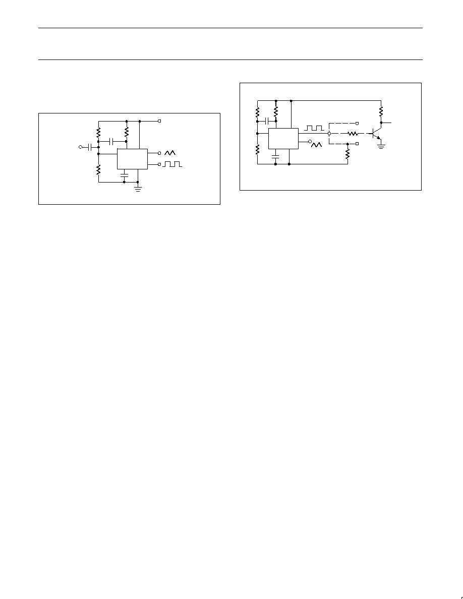
OPERATING INSTRUCTIONS
The NE/SE566 Function Generator is a general purpose
voltage-controlled oscillator designed for highly linear frequency
modulation. The circuit provides simultaneous square wave and
triangle wave outputs at frequencies up to 1MHz. A typical
connection diagram is shown in Figure 1. The control terminal (Pin
5) must be biased externally with a voltage (V
C
) in the range
V+
V
C
V+
where V
CC
is the total supply voltage. In Figure 1, the control
voltage is set by the voltage divider formed with R
2
and R
3
. The
modulating signal is then AC coupled with the capacitor C
2
. The
modulating signal can be direct coupled as well, if the appropriate
DC bias voltage is applied to the control terminal. The frequency is
given approximately by
f
O
+
2 [(V
)
)
*
(V
C
)]
R
1
C
1
V
)
and R
1
should be in the range 2k
< R
1
<20k
.
A small capacitor (typically 0.001
µ
F) should be connected between
Pins 5 and 6 to eliminate possible oscillation in the control current
source.
If the VCO is to be used to drive standard logic circuitry, it may be
desirable to use a dual supply as shown in Figure 2. In this case the
square wave output has the proper DC levels for logic circuitry. RTL
can be driven directly from Pin 3. For DTL or TTL gates, which
require a current sink of more than 1mA, it is usually necessary to
connect a 5k
resistor between Pin 3 and negative supply. This
increases the current sinking capability to 2mA. The third type of