 | –≠–ª–µ–∫—Ç—Ä–æ–Ω–Ω—ã–π –∫–æ–º–ø–æ–Ω–µ–Ω—Ç: NE567D | –°–∫–∞—á–∞—Ç—å:  PDF PDF  ZIP ZIP |
Document Outline
- DESCRIPTION
- FEATURES
- APPLICATIONS
- PIN CONFIGURATIONS
- BLOCK DIAGRAM
- EQUIVALENT SCHEMATIC
- ORDERING INFORMATION
- ABSOLUTE MAXIMUM RATINGS
- DC ELECTRICAL CHARACTERISTICS
- TYPICAL PERFORMANCE CHARACTERISTICS
- DESIGN FORMULAS
- PHASE-LOCKED LOOP TERMINOLOGY CENTER FREQUENCY (f O )
- Detection Bandwidth (BW)
- Lock Range
- Detection Band Skew
- OPERATING INSTRUCTIONS
- TYPICAL RESPONSE
- AVAILABLE OUTPUTS
- OPERATING PRECAUTIONS
- SPEED OF OPERATION
- OPTIONAL CONTROLS
- SENSITIVITY ADJUSTMENT
- CHATTER PREVENTION
- DETECTION BAND CENTERING (OR SKEW) ADJUSTMENT
- ALTERNATE METHOD OF BANDWIDTH REDUCTION
- OUTPUT LATCHING
- REDUCTION OF C1 VALUE
- PROGRAMMING
- TYPICAL APPLICATIONS
Philips Semiconductors Linear Products
Product specification
NE/SE567
Tone decoder/phase-locked loop
403
April 15, 1992
853-0124 06456
DESCRIPTION
The NE/SE567 tone and frequency decoder is a highly stable
phase-locked loop with synchronous AM lock detection and power
output circuitry. Its primary function is to drive a load whenever a
sustained frequency within its detection band is present at the
self-biased input. The bandwidth center frequency and output delay
are independently determined by means of four external
components.
FEATURES
∑
Wide frequency range (.01Hz to 500kHz)
∑
High stability of center frequency
∑
Independently controllable bandwidth (up to 14%)
∑
High out-band signal and noise rejection
∑
Logic-compatible output with 100mA current sinking capability
∑
Inherent immunity to false signals
∑
Frequency adjustment over a 20-to-1 range with an external
resistor
∑
Military processing available
APPLICATIONS
∑
Touch-Tone
Æ
decoding
∑
Carrier current remote controls
∑
Ultrasonic controls (remote TV, etc.)
∑
Communications paging
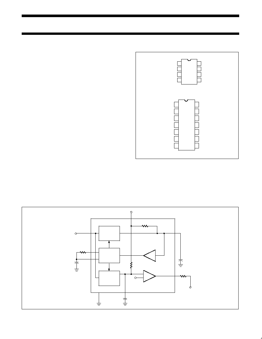
PIN CONFIGURATIONS
FE, D, N Packages
F Package
1
2
3
4
5
6
7
8
1
2
3
4
5
6
7
8
14
13
12
11
10
9
OUTPUT FILTER
CAPACITOR C3
LOW-PASS FILTER
CAPACITOR C2
INPUT
SUPPLY VOLTAGE V+
OUTPUT
GROUND
TIMING
ELEMENTS R1
AND C1
TIMING ELEMENT R1
OUTPUT
C3
NC
C2
INPUT
NC
VCC
GND
NC
NC
R1C1
R1
NC
NC
TOP VIEW
TOP VIEW
∑
Frequency monitoring and control
∑
Wireless intercom
∑
Precision oscillator
BLOCK DIAGRAM
Æ
Touch-Tone is a registered trademark of AT&T.
INPUT
V1
PHASE
DETECTOR
CURRENT
CONTROLLED
OSCILLATOR
QUADRATURE
PHASE
DETECTOR
AMP
AMP
LOOP
LOW
PASS
FILTER
3
5
6
7
1
8
2
4
3.9k
+
≠
+V
FILTER
C1
R1
R2
R3
RL
VREF
C2
C3 OUTPUT
Philips Semiconductors Linear Products
Product specification
NE/SE567
Tone decoder/phase-locked loop
April 15, 1992
404
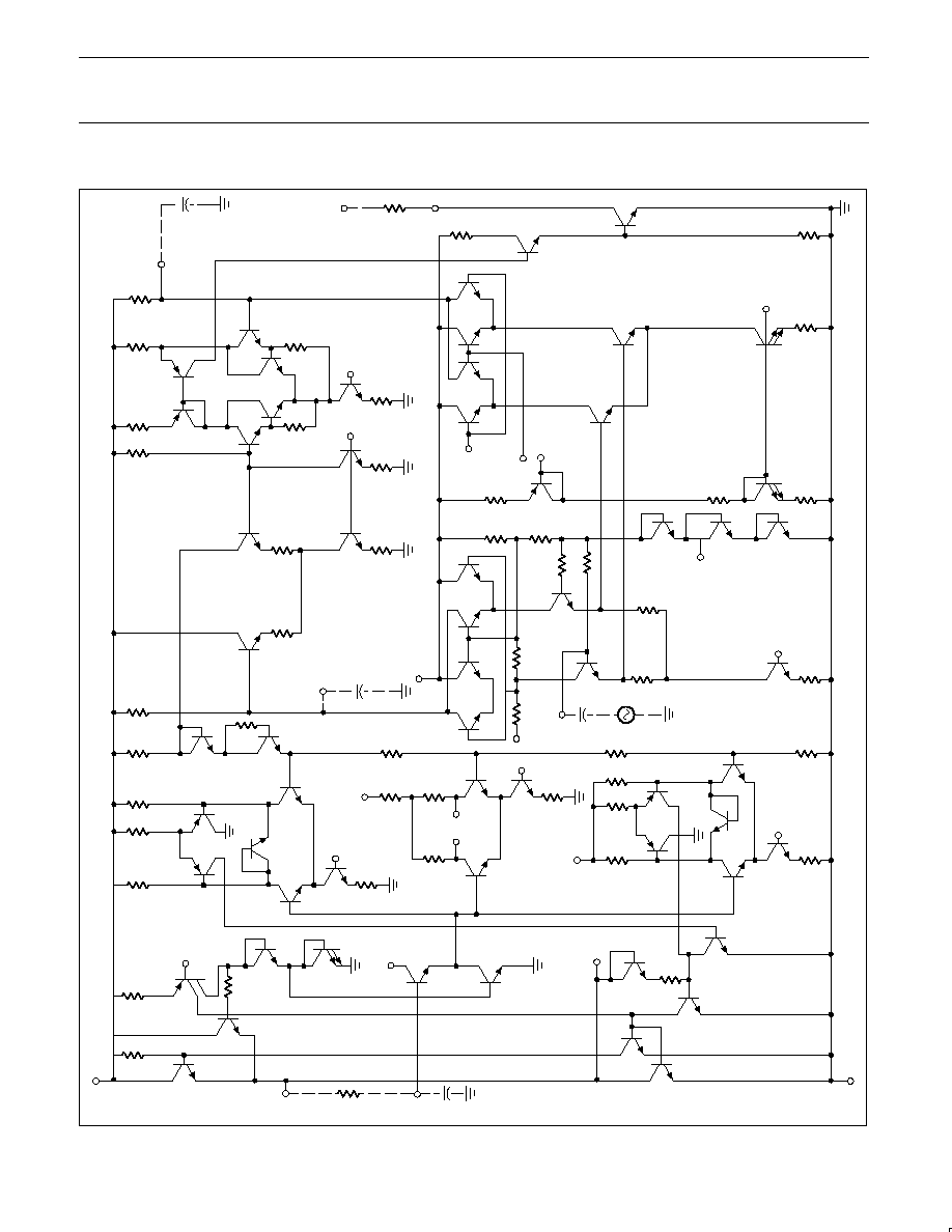
EQUIVALENT SCHEMATIC
≠V
4
R5
Q1
5
R1
6
C1
Q2
7
Q8
Q3
R6
Q10
D
R7
Q12
Q13
≠V
Q6
Q7
A
Q9
R4
Q5
R9
Q14
Q16
Q17
Q19
B
R19
R12
Q22
≠V
R15
Q25
Q24
Q26
Q27
Q28
Q29
B
R18
R10
R1
1
≠V
R20
R13
E
F
Q23
Q30
B
R14
R16
R17
R23
R24
R21
R2
10k
Q20
R26
Q21
R22
A
Q34
R29
3
C
V
i
2
C2
≠V
Q35
R30
R26
R27
Q33
Q36
Q37
R36
Q50
R37
Q62
V
ref
Q59
R40
F
E
R32
R48
21k
R48
21k
Q40
C
Q30
Q38
R36
R34
Q61
R36
Q16
Q18
Q31
B
R28
Q40
R33
R39
5k
R41
Q63
Q55
R48
Q60
C
R43
Q47
Q46
Q45
Q44
Q43
Q42
Q41
B
R44
Q62
Q61
R45
B
RL
≠V
R49
C3
1
R3
4.7k
R42
Q54
Q57
Q56
Q58
Q32
c
Philips Semiconductors Linear Products
Product specification
NE/SE567
Tone decoder/phase-locked loop
April 15, 1992
405
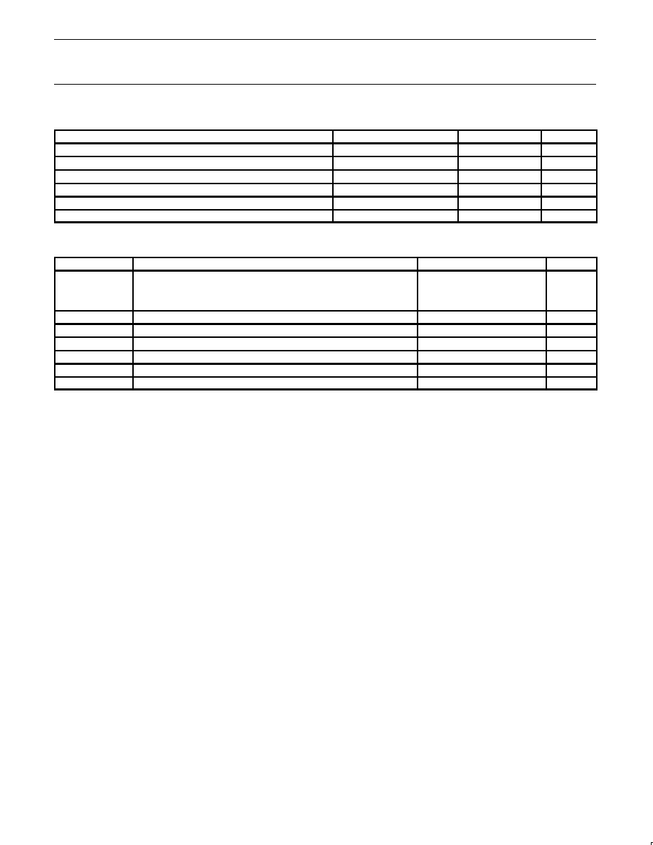
ORDERING INFORMATION
DESCRIPTION
TEMPERATURE RANGE
ORDER CODE
DWG #
8-Pin Plastic SO
0 to +70
∞
C
NE567D
0174C
14-Pin Cerdip
0 to +70
∞
C
NE567F
0581B
8-Pin Plastic DIP
0 to +70
∞
C
NE567N
0404B
8-Pin Plastic SO
-55
∞
C to +125
∞
C
SE567D
0174C
8-Pin Cerdip
-55
∞
C to +125
∞
C
SE567FE
0581B
8-Pin Plastic DIP
-55
∞
C to +125
∞
C
SE567N
0404B
ABSOLUTE MAXIMUM RATINGS
SYMBOL
PARAMETER
RATING
UNIT
T
A
Operating temperature
NE567
0 to +70
∞
C
SE567
-55 to +125
∞
C
V
CC
Operating voltage
10
V
V+
Positive voltage at input
0.5 +V
S
V
V-
Negative voltage at input
-10
V
DC
V
OUT
Output voltage (collector of output transistor)
15
V
DC
T
STG
Storage temperature range
-65 to +150
∞
C
P
D
Power dissipation
300
mW
Philips Semiconductors Linear Products
Product specification
NE/SE567
Tone decoder/phase-locked loop
April 15, 1992
406
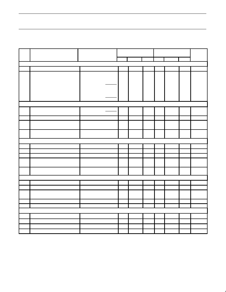
DC ELECTRICAL CHARACTERISTICS
V +=5.0V; T
A
=25
∞
C, unless otherwise specified.
SYM-
BOL
PARAMETER
TEST CONDITIONS
SE567
NE567
UNIT
Min
Typ
Max
Min
Typ
Max
Center frequency
1
f
O
Highest center frequency
500
500
kHz
f
O
Center frequency stability
2
-55 to +125
∞
C
35
±
140
35
±
140
ppm/
∞
C
0 to +70
∞
C
35
±
60
35
±
60
ppm/
∞
C
f
O
Center frequency distribution
f
O
+
100kHz
+
1
1.1R
1
C
1
-10
0
+10
-10
0
+10
%
f
O
Center frequency shift with supply
voltage
f
O
+
100kHz
+
1
1.1R
1
C
1
0.5
1
0.7
2
%/V
Detection bandwidth
BW
Largest detection bandwidth
f
O
+
100kHz
+
1
1.1R
1
C
1
12
14
16
10
14
18
% of f
O
BW
Largest detection bandwidth skew
2
4
3
6
% of f
O
BW
Largest detection bandwidth--
V
I
=300mV
RMS
±
0.1
±
0.1
%/
∞
C
variation with temperature
BW
Largest detection bandwidth--
V
I
=300mV
RMS
±
2
±
2
%/V
variation with supply voltage
Input
R
IN
Input resistance
15
20
25
15
20
25
k
V
I
Smallest detectable input voltage
4
I
L
=100mA, f
I
=f
O
20
25
20
25
mV
RMS
Largest no-output input voltage
4
I
L
=100mA, f
I
=f
O
10
15
10
15
mV
RMS
Greatest simultaneous out-band
+6
+6
dB
signal-to-in-band signal ratio
Minimum input signal to wide-band
noise ratio
B
n
=140kHz
-6
-6
dB
Output
Fastest on-off cycling rate
f
O
/20
f
O
/20
"1" output leakage current
V
8
=15V
0.01
25
0.01
25
µ
A
"0" output voltage
I
L
=30mA
0.2
0.4
0.2
0.4
V
I
L
=100mA
0.6
1.0
0.6
1.0
V
t
F
Output fall time
3
R
L
=50
30
30
ns
t
R
Output rise time
3
R
L
=50
150
150
ns
General
V
CC
Operating voltage range
4.75
9.0
4.75
9.0
V
Supply current quiescent
6
8
7
10
mA
Supply current--activated
R
L
=20k
11
13
12
15
mA
t
PD
Quiescent power dissipation
30
35
mW
NOTES:
1. Frequency determining resistor R
1
should be between 2 and 20k
2. Applicable over 4.75V to 5.75V. See graphs for more detailed information.
3. Pin 8 to Pin 1 feedback R
L
network selected to eliminate pulsing during turn-on and turn-off.
4. With R
2
=130k
from Pin 1 to V+. See Figure 1.
Philips Semiconductors Linear Products
Product specification
NE/SE567
Tone decoder/phase-locked loop
April 15, 1992
407
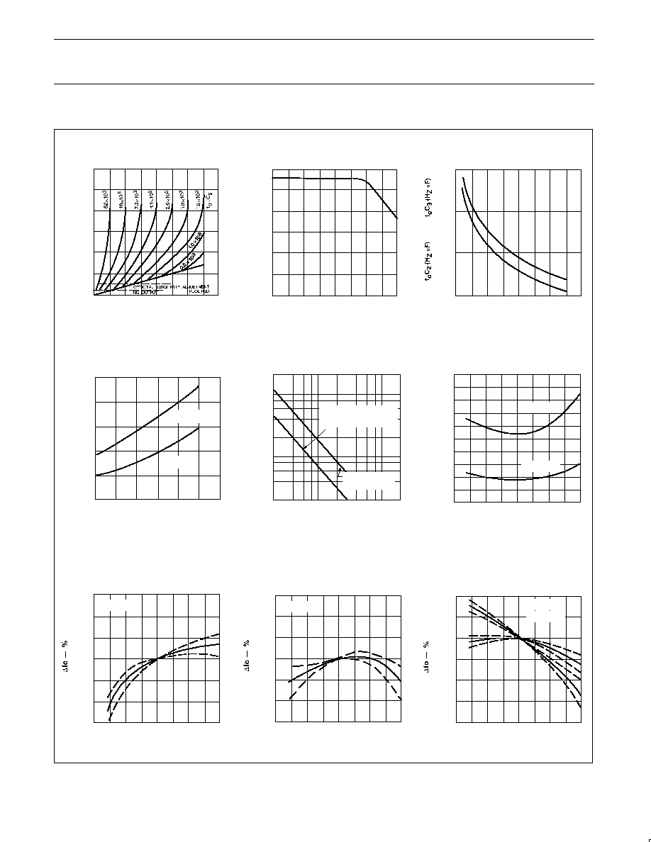
TYPICAL PERFORMANCE CHARACTERISTICS
Bandwidth vs Input
Signal Amplitude
Largest Detection bandwidth
vs Operating Frequency
Detection bandwidth as a
Function of C
2
and C
3
Typical Supply Current vs
Supply Voltage
Greatest Number of Cycles
Before Output
Typical Output Voltage vs
Temperature
Typical Frequency Drift
With Temperature
(Mean and SD)
Typical Frequency Drift
With Temperature
(Mean and SD)
Typical Frequency Drift
With Temperature
(Mean and SD)
300
250
200
150
100
50
0
0
2
4
6
8
10
12
14
16
INPUT
VOL
T
AGE -- mV
rms
BANDWIDTH -- % OF fO
CENTER FREQUENCY -- kHz
LARGEST
BANDWIDTH -- % OF f
15
10
5
0
0.1
1
10
100
1000
O
BANDWIDTH -- % OF fO
0
2
4
6
8
10
12
14
16
106
C3
C2
105
104
103
25
20
15
10
5
0
4
5
6
7
8
9
10
SUPPLY VOLTAGE -- V
CUPPL
Y
CURRENT
-- mA
QUIESCENT
CURRENT
NO LOAD
"ON" CURRENT
1.5
1.0
0.5
0
≠0.5
≠1.0
≠1.5
≠75
≠25
0
25
75
125
TEMPERATURE --
∞
C
TEMPERATURE --
∞
C
TEMPERATURE --
∞
C
+V = 4.75V
1.5
1.0
0.5
0
≠0.5
≠1.0
≠1.5
≠75
≠25
0
25
75
125
+V = 5.75V
5.5
2.5
0
≠2.5
≠5.0
≠7.5
≠10
≠75
≠25
0
25
75
125
(2)
(1)
+V = 7.0V (1)
+V = 9.0V (2)
1.0
0.9
0.8
0.7
0.6
0.5
0.4
0.3
0.2
0.1
0
≠75
≠25
0
25
75
125
TEMPERATURE --
∞
C
OUTPUT
VOL
T
AGE PIN 8 -- V
IL = 100mA
IL = 30mA
1000
500
300
100
50
30
10
CYCLES
BANDWIDTH -- % OF fO
1
5
10
50
100
BANDWIDTH LIMITED BY
EXTERNAL RESISTOR
(MINIMUM C2)
BANDWIDTH
LIMITED BY (C2)
(Hz * F)
µ

Philips Semiconductors Linear Products
Product specification
NE/SE567
Tone decoder/phase-locked loop
April 15, 1992
408
TYPICAL PERFORMANCE CHARACTERISTICS
(Continued)
Center Frequency Temperature
Coefficient
(Mean and SD)
Center Frequency
Shift With Supply
Voltage Change vs
Operating Frequency
Typical Bandwidth Variation
Temperature
100
0
≠100
≠200
≠300
4.5
5.0
5.5
6.0
6.5
7.0
SUPPLY VOLTAGE -- V
TEMPERA
TURE COEFFICIENT
-- ppm/ C
∞
t = 0
∞
C to 70
∞
C
1.0
0.9
0.8
0.7
0.6
0.5
0.4
0.3
0.2
0.1
0
1
2
3 4 5
10
20
40
100
CENTER FREQUENCY -- kHz
D
t
O
t
O
V
*
% V
15.0
12.5
10.0
7.5
5.0
2.5
0
≠75
≠25
0
25
75
125
TEMPERATURE ≠
∞
C
BANDWIDTH AT 25
∞
C
2
4
6
8
10
12
14
BANDWIDTH -- % OF f
O
DESIGN FORMULAS
f
O
[
1
1.1R
1
C
1
BW
[
1070
V
I
f
O
C
2
in % of f
O
V
I
v
200mV
RMS
Where
V
I
=Input voltage (V
RMS
)
C
2
=Low-pass filter capacitor (
µ
F)
PHASE-LOCKED LOOP TERMINOLOGY CENTER
FREQUENCY (f
O
)
The free-running frequency of the current controlled oscillator (CCO)
in the absence of an input signal.
Detection Bandwidth (BW)
The frequency range, centered about f
O
, within which an input signal
above the threshold voltage (typically 20mV
RMS
) will cause a logical
zero state on the output. The detection bandwidth corresponds to
the loop capture range.
Lock Range
The largest frequency range within which an input signal above the
threshold voltage will hold a logical zero state on the output.
Detection Band Skew
A measure of how well the detection band is centered about the
center frequency, f
O
. The skew is defined as (f
MAX
+f
MIN
-2f
O
)/2f
O
where fmax and fmin are the frequencies corresponding to the
edges of the detection band. The skew can be reduced to zero if
necessary by means of an optional centering adjustment.
OPERATING INSTRUCTIONS
Figure 1 shows a typical connection diagram for the 567. For most
applications, the following three-step procedure will be sufficient for
choosing the external components R
1
, C
1
, C
2
and C
3
.
1. Select R1 and C1 for the desired center frequency. For best
temperature stability, R1 should be between 2K and 20K ohm,
and the combined temperature coefficient of the R1C1 product
should have sufficient stability over the projected temperature
range to meet the necessary requirements.
2. Select the low-pass capacitor, C
2
, by referring to the Bandwidth
versus Input Signal Amplitude graph. If the input amplitude
Variation is known, the appropriate value of f
O
C
2
necessary to
give the desired bandwidth may be found. Conversely, an area of
operation may be selected on this graph and the input level and
C2 may be adjusted accordingly. For example, constant
bandwidth operation requires that input amplitude be above
200mV
RMS
. The bandwidth, as noted on the graph, is then
controlled solely by the f
O
C
2
product (f
O
(Hz), C2(
µ
F)).

Philips Semiconductors Linear Products
Product specification
NE/SE567
Tone decoder/phase-locked loop
April 15, 1992
409
TYPICAL RESPONSE
Response to 100mV
RMS
Tone Burst
Response to Same Input Tone Burst
With Wideband Noise
INPUT
OUTPUT
OUTPUT
INPUT
NOTES:
NOTE:
RL = 100
S/N = ≠6dB
Noise Bandwidth = 140Hz
RL = 100
3. The value of C3 is generally non-critical. C3 sets the band edge
of a low-pass filter which attenuates frequencies outside the
detection band to eliminate spurious outputs. If C3 is too small,
frequencies just outside the detection band will switch the output
stage on and off at the beat frequency, or the output may pulse
on and off during the turn-on transient. If C3 is too large, turn-on
and turn-off of the
Figure 1.
INPUT
3
5
6
2
7
1
8
4
+V
+V
OUTPUT
FILTER
LOW
PASS
FILTER
567
R1
RL
R2
C3
C2
C1
f
O
+
1
R
1
C
1
output stage will be delayed until the voltage on C
3
passes the
threshold voltage. (Such delay may be desirable to avoid spurious
outputs due to transient frequencies.) A typical minimum value for
C
3
is 2C
2
.
4. Optional resistor R2 sets the threshold for the largest "no output"
input voltage. A value of 130k
is used to assure the tested limit
of 10mV
RMS
min. This resistor can be referenced to ground for
increased sensitivity. The explanation can be found in the
"optional controls" section which follows.
AVAILABLE OUTPUTS
(Figure 1)
The primary output is the uncommitted output transistor collector,
Pin 8. When an in-band input signal is present, this transistor
saturates; its collector voltage being less than 1.0 volt (typically
0.6V) at full output current (100mA). The voltage at Pin 2 is the
phase detector output which is a linear function of frequency over
the range of 0.95 to 1.05 f
O
with a slope of about 20mV per percent
of frequency deviation. The average voltage at Pin 1 is, during lock,
a function of the in-band input amplitude in accordance with the
transfer characteristic given. Pin 5 is the controlled oscillator square
wave output of magnitude (+V -2V
BE
)
(+V-1.4V) having a DC
average of +V/2. A 1k
load may be driven from pin 5. Pin 6 is an
exponential triangle of 1V
P-P
with an average DC level of +V/2. Only
high impedance loads may be
Figure 2. Typical Output Response
THRESHOLD VOLTAGE
VREF
4.0
3.5
3.0
2.5
0
100
200mVrms
IN-BAND
INPUT
VOLTAGE
PIN 1
VOLTAGE
(AVG)
f1 = fO
7%
BW
VCE (SAT) < 1.0V
14%
V+
0
3.9V
3.8V
3.7V
1.1fO
fO
0.9fO
LOW PASS
FILTER
(PIN 2)
OUTPUT
(PIN 8)
Philips Semiconductors Linear Products
Product specification
NE/SE567
Tone decoder/phase-locked loop
April 15, 1992
410
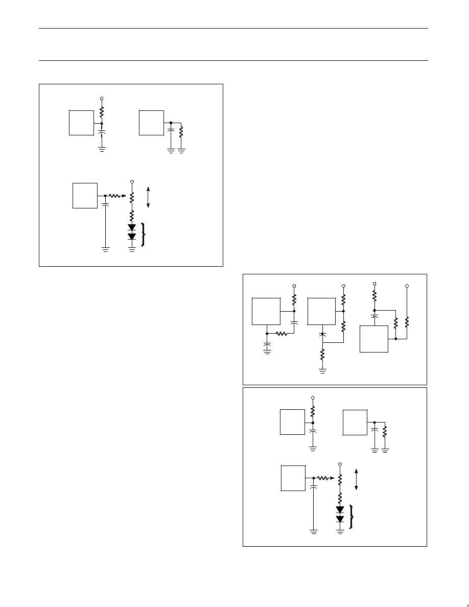
Figure 3. Sensitivity Adjust
567
567
567
DECREASE
SENSITIVITY
INCREASE
SENSITIVITY
V+
R
R
1
1
1
SILICON
DIODES FOR
TEMPERATURE
COMPENSATION
(OPTIONAL)
2.5k
1.0k
50k
C3
C3
C3
RB
RC
V+
DECREASE
SENSITIVITY
INCREASE
SENSITIVITY
RA
connected to pin 6 without affecting the CCO duty cycle or
temperature stability.
OPERATING PRECAUTIONS
A brief review of the following precautions will help the user achieve
the high level of performance of which the 567 is capable.
1. Operation in the high input level mode (above 200mV) will free
the user from bandwidth variations due to changes in the in-band
signal amplitude. The input
stage is now limiting, however, so that out-band signals or high
noise levels can cause an apparent bandwidth reduction as the
inband signal is suppressed. Also, the limiting action will create
in-band components from sub-harmonic signals, so the 567
becomes sensitive to signals at f
O
/3, f
O
/5, etc.
2. The 567 will lock onto signals near (2n+1) f
O
, and will give an
output for signals near (4n+1) f
O
where n=0, 1, 2, etc. Thus,
signals at 5f
O
and 9f
O
can cause an unwanted output. If such
signals are anticipated, they should be attenuated before
reaching the 567 input.
3. Maximum immunity from noise and out-band signals is afforded
in the low input level (below 200mV
RMS
) and reduced bandwidth
operating mode. However, decreased loop damping causes the
worst-case lock-up time to increase, as shown by the Greatest
Number of Cycles Before Output vs Bandwidth graph.
4. Due to the high switching speeds (20ns) associated with 567
operation, care should be taken in lead routing. Lead lengths
should be kept to a minimum. The power supply should be
adequately bypassed close to the 567 with a 0.01
µ
F or greater
capacitor; grounding paths should be carefully chosen to avoid
ground loops and unwanted voltage variations. Another factor
which must be considered is the effect of load energization on
the power supply. For example, an incandescent lamp typically
draws 10 times rated current at turn-on. This can be somewhat
greater when the output stage is made less sensitive, rejection of
third harmonics or in-band harmonics (of lower frequency
signals) is also improved.
cause supply voltage fluctuations which could, for example, shift the
detection band of narrow-band systems sufficiently to cause
momentary loss of lock. The result is a low-frequency oscillation into
and out of lock. Such effects can be prevented by supplying heavy
load currents from a separate supply or increasing the supply filter
capacitor.
SPEED OF OPERATION
Minimum lock-up time is related to the natural frequency of the loop.
The lower it is, the longer becomes the turn-on transient. Thus,
maximum operating speed is obtained when C
2
is at a minimum.
When the signal is first applied, the phase may be such as to initially
drive the controlled oscillator away from the incoming frequency
rather than toward it. Under this condition, which is of course
unpredictable, the lock-up transient is at its worst and the theoretical
minimum lock-up time is not achievable. We must simply wait for the
transient to die out.
The following expressions give the values of C
2
and C
3
which allow
highest operating speeds for various band center frequencies. The
minimum rate at which digital information may be detected without
information loss due to the turn-on transient or output chatter is
about 10 cycles per bit, corresponding to an information transfer rate
of f
O
/10 baud.
Rf
Figure 4. Chatter Prevention
567
V+
8
Cf
LOWER VALUE OF Cf
RL
Rf*
10k
*OPTIONAL - PERMITS
C3
567
V+
8
200 TO
RL
RA
C3
1
1k
10k
567
V+
8
1
10k
Rf
RL
V+
200 TO 1k
RA
1
Figure 5. Skew Adjust
567
567
567
V+
R
R
2
2
1
SILICON
DIODES FOR
TEMPERATURE
COMPENSATION
(OPTIONAL)
2.5k
1.0k
50k
C2
C2
C2
RB
RC
V+
RA
RAISES fO
LOWERS fO
RAISES fO
RAISES fO
LOWERS fO
Philips Semiconductors Linear Products
Product specification
NE/SE567
Tone decoder/phase-locked loop
April 15, 1992
411
C
2
+
130
f
O
m
F
C
3
+
260
f
O
m
F
In cases where turn-off time can be sacrificed to achieve fast
turn-on, the optional sensitivity adjustment circuit can be used to
move the quiescent C
3
voltage lower (closer to the threshold
voltage). However, sensitivity to beat frequencies, noise and
extraneous signals will be increased.
OPTIONAL CONTROLS
(Figure 3)
The 567 has been designed so that, for most applications, no
external adjustments are required. Certain applications, however,
will be greatly facilitated if full advantage is taken of the added
control possibilities available through the use of additional external
components. In the diagrams given, typical
values are suggested where applicable. For best results the
resistors used, except where noted, should have the same
temperature coefficient. Ideally, silicon diodes would be
low-resistivity types, such as forward-biased transistor base-emitter
junctions. However, ordinary low-voltage diodes should be adequate
for most applications.
DETECTION BAND -- % OF fO
Figure 6. BW Reduction
NOTE:
130
f
O
10k
)
R
R
t
C
2
t
1300
f
O
10k
)
R
R
Adjust control for symmetry of detection band edges
about fO.
250
200
150
100
50
0
0
2
4
6
8
10
12
14
16
INPUT VOL
T
AGE MV -- RMS
0.5k 0.9k 1.4k
1.9k
2.5k 3.2k
4.0k
10k
20k
100k
R
OPTIONAL SILICON
DIODES FOR
TEMPERATURE
COMPENSATION
PIN 2
567
V+
C2
RA
RB
RC
R
+
R
A
)
R
B
R
C
R
B
)
R
C
50k
SENSITIVITY ADJUSTMENT
(Figure 3)
When operated as a very narrow-band detector (less than 8
percent), both C
2
and C
3
are made quite large in order to improve
noise and out-band signal rejection. This will inevitably slow the
response time. If, however, the output stage is biased closer to the
threshold level, the turn-on time can be
improved. This is accomplished by drawing additional current to
terminal 1. Under this condition, the 567 will also give an output for
lower-level signals (10mV or lower).
By adding current to terminal 1, the output stage is biased further
away from the threshold voltage. This is most useful when, to obtain
maximum operating speed, C
2
and C
3
are made very small.
Normally, frequencies just outside the detection band could cause
false outputs under this condition. By desensitizing the output stage,
the out-band beat notes do not feed through to the output stage.
Since the input level must
Figure 7. Output Latching
NOTE:
CA prevents latch-up when power supply is turned on.
V+
C3
RL
V+
CA
RA
10k
567 8
1
UNLATCH
20k
Rf
V+
567 8
1
20k
C3
RL
Rf
UNLATCH
V+

Philips Semiconductors Linear Products
Product specification
NE/SE567
Tone decoder/phase-locked loop
April 15, 1992
412
CHATTER PREVENTION
(Figure 4)
Chatter occurs in the output stage when C
3
is relatively small, so
that the lock transient and the AC components at the quadrature
phase detector (lock detector) output cause the output stage to
move through its threshold more than once. Many loads, for
example lamps and relays, will not respond to the chatter. However,
logic may recognize the chatter as a series of outputs. By feeding
the output stage output back to its input (Pin 1) the chatter can be
eliminated. Three schemes for doing this are given in Figure 4. All
operate by feeding the first output step (either on or off) back to the
input, pushing the input past the threshold until the transient
conditions are over. It is only necessary to assure that the feedback
time constant is not so large as to prevent operation at the highest
anticipated speed. Although chatter can always be eliminated by
making C
3
large, the feedback circuit will enable faster operation of
the 567 by allowing C
3
to be kept small. Note that if the feedback
time constant is made quite large, a short burst at the input
frequency can be stretched into a long output pulse. This may be
useful to drive, for example, stepping relays.
DETECTION BAND CENTERING (OR SKEW)
ADJUSTMENT
(Figure 5)
When it is desired to alter the location of the detection band
(corresponding to the loop capture range) within the lock range, the
circuits shown above can be used. By moving the detection band to
one edge of the range, for example, input signal variations will
expand the detection band in only one direction. This may prove
useful when a strong but undesirable signal is expected on one side
or the other of the center frequency. Since R
B
also alters the duty
cycle slightly, this method may be used to obtain a precise duty
cycle when the 567 is used as an oscillator.
ALTERNATE METHOD OF BANDWIDTH
REDUCTION
(Figure 6)
Although a large value of C
2
will reduce the bandwidth, it also
reduces the loop damping so as to slow the circuit response time.
This may be undesirable. Bandwidth can be reduced by reducing
the loop gain. This scheme will improve damping and permit faster
operation under narrow-band conditions. Note that the reduced
impedance level at terminal 2 will require that a larger value of C
2
be
used for a given filter cutoff
frequency. If more than three 567s are to be used, the network of R
B
and R
C
can be eliminated and the R
A
resistors connected together.
A capacitor between this junction and ground may be required to
shunt high frequency components.
OUTPUT LATCHING
(Figure 7)
To latch the output on after a signal is received, it is necessary to
provide a feedback resistor around the output stage (between Pins 8
and 1). Pin 1 is pulled up to unlatch the output stage.
REDUCTION OF C1 VALUE
For precision very low-frequency applications, where the value of C
1
becomes large, an overall cost savings may be achieved by
inserting a voltage-follower between the R
1
C
1
junction and Pin 6,
so as to allow a higher value of R
1
and a lower value of C
1
for a
given frequency.
PROGRAMMING
To change the center frequency, the value of R
1
can be changed
with a mechanical or solid state switch, or additional C
1
capacitors
may be added by grounding them through saturating NPN
transistors.

Philips Semiconductors Linear Products
Product specification
NE/SE567
Tone decoder/phase-locked loop
April 15, 1992
413
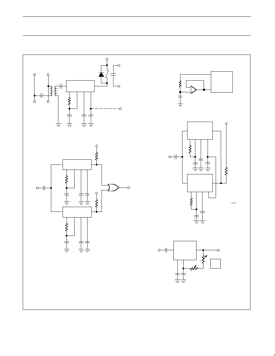
TYPICAL APPLICATIONS
Touch-Tone
Æ
Decoder
NOTES:
Component values (Typical)
R1 = 26.8 to 15k
R2 = 24.7k
R3 = 20k
C1 = 0.10mF
C2 = 1.0mF 5V
C3 = 2.2mF 6V
C4 = 250
µ
F 6V
DIGIT
1
2
3
4
5
6
7
8
9
0
*
567
897Hz
567
770Hz
567
852Hz
567
941Hz
567
1209Hz
567
1336Hz
567
1477Hz
+
+
+
+
+
+
+
R3
R2
R1
C1
C3
C2
Philips Semiconductors Linear Products
Product specification
NE/SE567
Tone decoder/phase-locked loop
April 15, 1992
414
TYPICAL APPLICATIONS
(Continued)
NOTES:
R2 = R1/5
Adjust R1 so that
= 90
∞
with control midway.
NOTES:
1. Resistor and capacitor values chosen for desired frequencies and bandwidth.
2. If C3 is made large so as to delay turn-on of the top 567, decoding of sequential (f1 f2) tones is possible.
Dual-Tone Decoder
24% Bandwidth Tone Decoder
Precision VLF
Carrier-Current Remote Control or Intercom
0
∞
to 180
∞
Phase Shifter
AUDIO OUT
(IF INPUT IS
FREQUENCY
MODULATED)
LOAD
+5 TO 15V
567
3
5
6
2
1
8
60Hz AC LINE
500pF
50≠200VRMS
fO
100kHz
C2
C3
C1
0.004mfd
.006
.02
K1
C4
27pF
1:1
R1
2.5k
567
5
6
5741
≠
+
+
C1
R1
INPUT
CHANNEL
OR RECEIVER
567
3
5
6
2
1
8
567
3
5
6
2
1
8
C1
C2
C3
C'1
C'2
C'3
R1
R'1
NOR
20k
20k
+V
+V
VO
f1
f2
OUTPUT
(INTO 1k
OHM MIN.
LOAD)
567
3
5
6
2
R1
f2
C1
C2
100mv (pp)
SQUARE OR
50mVRMS
SINE INPUT
+90
∞
PHASE
SHIFT
567
3
5
6
2
1
8
567
3
5
6
2
1
8
INPUT SIGNAL
(>100mVrms)
+V
RL
R1
R'1
C'1
C'2
C1
C2
C3
C
2
+
C
2
+
130
f
O
(mfd)
C
1
+
C
1
R
1
+
1.12R
1

Philips Semiconductors Linear Products
Product specification
NE/SE567
Tone decoder/phase-locked loop
April 15, 1992
415
TYPICAL APPLICATIONS
(Continued)
Oscillator With Quadrature Output
Oscillator With Double Frequency
Output
Precision Oscillator With 20ns
Switching
Pulse Generator With 25% Duty Cycle
Precision Oscillator to Switch 100mA
Loads
Pulse Generator
CONNECT PIN 3
TO 2.8V TO
INVERT OUTPUT
567
3
2
6
5
8
+
RL
RL > 1000
R1
CL
80
∞
+
RL
R1
10k
C1
C2
567
3
2
6
5
8
fO
567
2
6
5
RL > 1000
R1
C1
C2
VCO
TERMINAL
(
±
6%)
+
567
1
3
6
5
8
RL
R1
C1
10k
+
567
1
2
6
5
8
RL
R1
C1
C2
VCO
TERMINAL
(
±
6%)
567
6
5
OUTPUT
DUTY
CYCLE
ADJUST
C1
1k
(MIN)
100k