 | –≠–ª–µ–∫—Ç—Ä–æ–Ω–Ω—ã–π –∫–æ–º–ø–æ–Ω–µ–Ω—Ç: NE570D | –°–∫–∞—á–∞—Ç—å:  PDF PDF  ZIP ZIP |
Document Outline
- GENERAL DESCRIPTION
- FEATURES
- APPLICATIONS
- ORDERING INFORMATION
- BLOCK DIAGRAM
- ABSOLUTE MAXIMUM RATINGS
- AC ELECTRICAL CHARACTERISTICS
- CIRCUIT DESCRIPTION
- TYPICAL TEST CIRCUIT
- INTRODUCTION
- CIRCUIT BACKGROUND
- BASIC CIRCUIT HOOK-UP AND OPERATION
- CIRCUIT DETAILSÑRECTIFIER
- VARIABLE GAIN CELL
- OPERATIONAL AMPLIFIER
- RESISTORS
- PACKAGE OUTLINE
- REVISION HISTORY
- Data sheet status
- Definitions
- Disclaimers

Philips
Semiconductors
NE570
Compandor
Product data
Supersedes data of 1990 Jun 07
2003 Apr 03
INTEGRATED CIRCUITS

Philips Semiconductors
Product data
NE570
Compandor
2
2003 Apr 03
GENERAL DESCRIPTION
The NE570 is a versatile low cost dual gain control circuit in which
either channel may be used as a dynamic range compressor or
expandor. Each channel has a full-wave rectifier to detect the
average value of the signal, a linerarized temperature-compensated
variable gain cell, and an operational amplifier.
The NE570 is well suited for use in cellular radio and radio
communications systems, modems, telephone, and satellite
broadcast/receive audio systems.
FEATURES
∑
Complete compressor and expandor in one IC
∑
Temperature compensated
∑
Greater than 110 dB dynamic range
∑
Operates down to 6 V
DC
∑
System levels adjustable with external components
∑
Distortion may be trimmed out
APPLICATIONS
∑
Cellular radio
∑
Telephone trunk comandor
∑
High level limiter
∑
Low level expandor--noise gate
∑
Dynamic noise reduction systems
∑
Voltage-controlled amplifier
∑
Dynamic filters
PIN CONFIGURATION
RECT_CAP_1
RECT_IN_1
G_CELL_IN_1
GND
RECT_CAP_2
RECT_IN_2
V
CC
1
2
3
4
5
6
7
8
9
10
11
12
13
14
16
15
RES_R3_1
OUTPUT_1
THD_TRIM_1
RES_R3_2
OUTPUT_2
THD_TRIM_2
TOP VIEW
SR02503
NE570D
INV_IN_1
INV_IN_2
G_CELL_IN_2
Figure 1. Pin configuration.
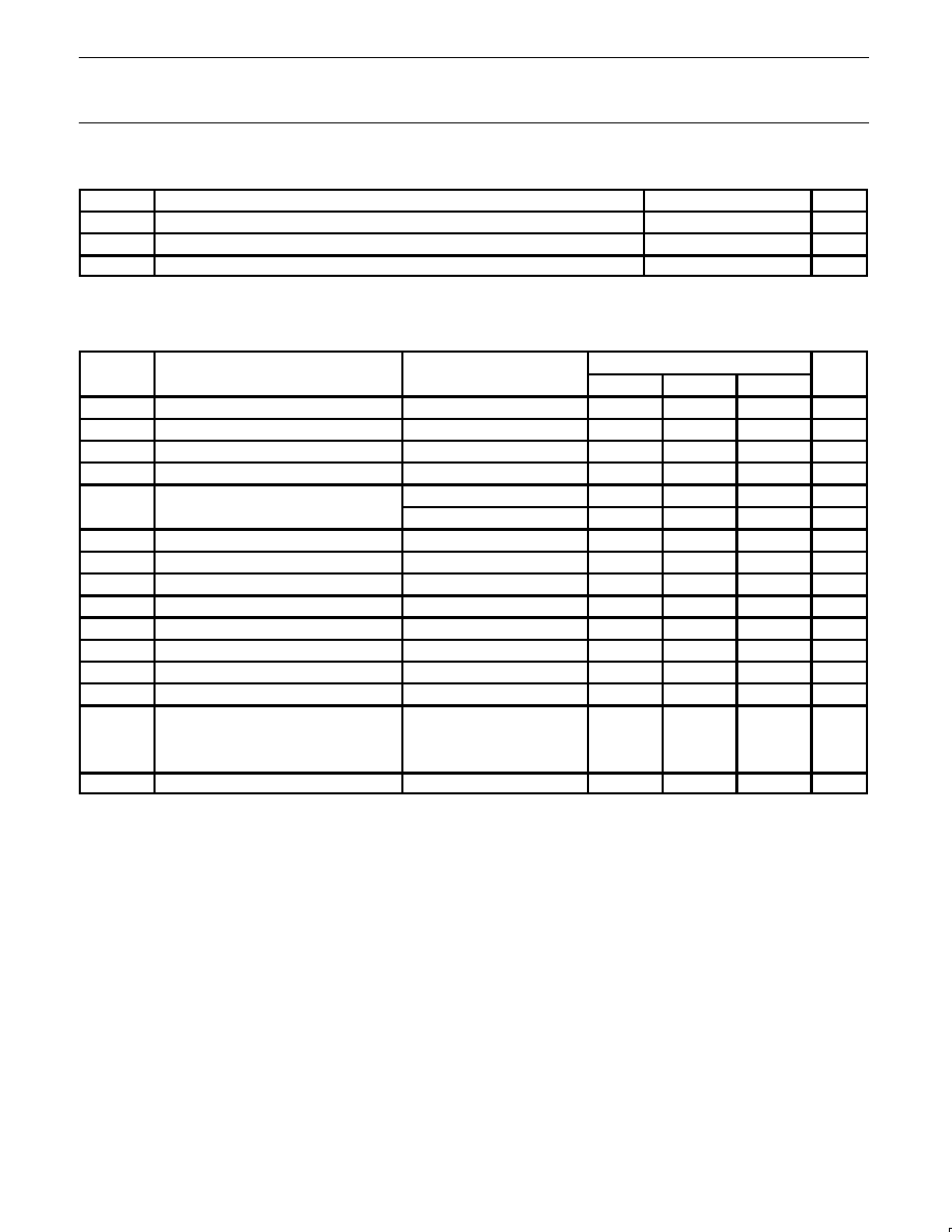
ORDERING INFORMATION
Type number
Package
Temperature range
Name
Description
Version
NE570D
SO16
plastic small outline package; 16 leads; body width 7.5 mm
SOT162-1
0
∞
C to +70
∞
C
BLOCK DIAGRAM
G CELL IN
RECT IN
V
REF
1.8 V
THD TRIM
RECT CAP
R3
INVERTER IN
OUTPUT
+
≠
SR02507
R2 20 k
R1 10 k
RECTIFIER
VARIABLE
GAIN
R4
30 k
R3
20 k
Figure 2. Block diagram
Philips Semiconductors
Product data
NE570
Compandor
2003 Apr 03
3
ABSOLUTE MAXIMUM RATINGS
SYMBOL
PARAMETER
RATING
UNITS
V
CC
Maximum operating voltage
24
V
DC
T
amb
Operating ambient temperature range
0 to +70
∞
C
P
D
Power dissipation
400
mW
AC ELECTRICAL CHARACTERISTICS
V
CC
= +6 V, T
amb
= 25
∞
C; unless otherwise stated.
SYMBOL
PARAMETER
TEST CONDITIONS
LIMITS
UNITS
SYMBOL
PARAMETER
TEST CONDITIONS
MIN
TYP
MAX
UNITS
V
CC
Supply voltage
6
≠
24
V
I
CC
Supply current
No signal
≠
3.2
4.8
mA
I
OUT
Output current capability
±
20
≠
≠
mA
SR
Output slew rate
≠
±
0.5
≠
V/
µ
s
Gain cell distortion
2
Untrimmed
≠
0.3
1.0
%
Trimmed
≠
0.05
≠
%
Resistor tolerance
≠
±
5
±
15
%
Internal reference voltage
1.7
1.8
1.9
V
Output DC shift
3
Untrimmed
≠
±
20
±
100
mV
Expandor output noise
No signal, 15 Hz to 20 kHz
1
≠
20
45
µ
V
Unity gain level
5
≠1
0
+1
dBm
Gain change
2, 4
T
amb
= 0
∞
C to +70
∞
C
≠
±
0.1
±
0.2
dB
Reference drift
4
T
amb
= 0
∞
C to +70
∞
C
≠
±
5
±
10
mV
Resistor drift
4
T
amb
= 0
∞
C to +70
∞
C
≠
+1, ≠0
≠
%
Tracking error (measured relative to value
Rectifier input
Tracking error (measured relative to value
at unity gain) equals [V
O
≠ V
O
(unity gain)]
dB
V dB
V
2
= +6 dBm, V
1
= 0 dB
≠
±
0.2
≠
dB
dB ≠ V
2
dBm
V
2
= -30dBm, V
1
= 0dB
≠
+0.2
≠0.5, +1
dB
Channel separation
≠
60
≠
dB
NOTES:
1. Input to V
1
and V
2
grounded.
2. Measured at 0 dBm, 1 kHz.
3. Expandor AC input change from no signal to 0 dBm.
4. Relative to value at T
amb
= 25
∞
C.
5. 0 dB = 775 mV
RMS
.

Philips Semiconductors
Product data
NE570
Compandor
2003 Apr 03
4
CIRCUIT DESCRIPTION
The NE570 compandor building blocks, as shown in the block
diagram, are a full-wave rectifier, a variable gain cell, an operational
amplifier and a bias system. The arrangement of these blocks in the
IC result in a circuit which can perform well with few external
components, yet can be adapted to many diverse applications.
The full-wave rectifier rectifies the input current which flows from the
rectifier input, to an internal summing node which is biased at V
REF
.
The rectified current is averaged on an external filter capacitor tied
to the C
RECT
terminal, and the average value of the input current
controls the gain of the variable gain cell. The gain will thus be
proportional to the average value of the input signal for
capacitively-coupled voltage inputs as shown in the following
equation. Note that for capacitively-coupled inputs there is no offset
voltage capable of producing a gain error. The only error will come
from the bias current of the rectifier (supplied internally) which is
less than 0.1
µ
A.
G
T
|V
IN
*
V
REF
| avg
R
1
or
G
T
| V
IN
| avg
R
1
The speed with which gain changes to follow changes in input signal
levels is determined by the rectifier filter capacitor. A small capacitor
will yield rapid response but will not fully filter low frequency signals.
Any ripple on the gain control signal will modulate the signal passing
through the variable gain cell. In an expander or compressor
application, this would lead to third harmonic distortion, so there is a
trade-off to be made between fast attack and decay times and
distortion. For step changes in amplitude, the change in gain with
time is shown by this equation.
G(t)
+
(G
initial
*
G
final
)
e
*
t
t )
G
final
;
t +
10k
C
RECT
The variable gain cell is a current-in, current-out device with the ratio
I
OUT
/I
IN
controlled by the rectifier. I
IN
is the current which flows from
the
G input to an internal summing node biased at V
REF
. The
following equation applies for capacitively-coupled inputs. The
output current, I
OUT
, is fed to the summing node of the op amp.
I
IN
+
V
IN
*
V
REF
R
2
+
V
IN
R
2
A compensation scheme built into the
G cell compensates for
temperature and cancels out odd harmonic distortion. The only
distortion which remains is even harmonics, and they exist only
because of internal offset voltages. The THD trim terminal provides
a means for nulling the internal offsets for low distortion operation.
The operational amplifier (which is internally compensated) has the
non-inverting input tied to V
REF
, and the inverting input connected to
the
G cell output as well as brought out externally. A resistor, R
3
, is
brought out from the summing node and allows compressor or
expander gain to be determined only by internal components.
The output stage is capable of
±
20 mA output current. This allows a
+13 dBm (3.5 V
RMS
) output into a 300
load which, with a series
resistor and proper transformer, can result in +13 dBm with a 600
output impedance.
A bandgap reference provides the reference voltage for all summing
nodes, a regulated supply voltage for the rectifier and
G cell, and a
bias current for the
G cell. The low tempco of this type of reference
provides very stable biasing over a wide temperature range.
The typical performance characteristics illustration shows the basic
input-output transfer curve for basic compressor or expander
circuits.
+20
+10
0
≠10
≠20
≠30
≠40
≠50
≠60
≠70
≠80
≠40
≠30
≠20
≠10
0
+10
COMPRESSOR OUTPUT LEVEL
OR
EXPANDOR INPUT LEVEL (dBm)
COMPRESSOR
INPUT
LEVEL
OR EXP
ANDOR
OUTPUT
LEVEL
(dBm)
SR00677
Figure 3. Basic input-output transfer curve
TYPICAL TEST CIRCUIT
13
2, 15
4
1, 16
5, 12
8, 9
7, 10
6, 11
V
1
V
2
V
O
V
CC
= 15 V
V
REF
10
µ
F
0.1
µ
F
SR02508
200 pF
8.2 k
2.2
µ
F
≠
+
30 k
20 k
G
10 k
20 k
2.2
µ
F
3, 14
2.2
µ
F
Figure 4. Typical Test Circuit

Philips Semiconductors
Product data
NE570
Compandor
2003 Apr 03
5
INTRODUCTION
Much interest has been expressed in high performance electronic
gain control circuits. For non-critical applications, an integrated
circuit operational transconductance amplifier can be used, but
when high-performance is required, one has to resort to complex
discrete circuitry with many expensive, well-matched components.
This paper describes an inexpensive integrated circuit, the NE570
Compandor, which offers a pair of high performance gain control
circuits featuring low distortion (<0.1 %), high signal-to-noise ratio
(90 dB), and wide dynamic range (110 dB).
CIRCUIT BACKGROUND
The NE570 Compandor was originally designed to satisfy the
requirements of the telephone system. When several telephone
channels are multiplexed onto a common line, the resulting
signal-to-noise ratio is poor and companding is used to allow a wider
dynamic range to be passed through the channel. Figure 5
graphically shows what a compandor can do for the signal-to-noise
ratio of a restricted dynamic range channel. The input level range of
+20 dB to ≠80 dB is shown undergoing a 2-to-1 compression where
a 2 dB input level change is compressed into a 1 dB output level
change by the compressor. The original 100 dB of dynamic range is
thus compressed to a 50 dB range for transmission through a
restricted dynamic range channel. A complementary expansion on
the receiving end restores the original signal levels and reduces the
channel noise by as much as 45 dB.
The significant circuits in a compressor or expander are the rectifier
and the gain control element. The phone system requires a simple
full-wave averaging rectifier with good accuracy, since the rectifier
accuracy determines the (input) output level tracking accuracy. The
gain cell determines the distortion and noise characteristics, and the
phone system specifications here are very loose. These specs could
have been met with a simple operational transconductance
multiplier, or OTA, but the gain of an OTA is proportional to
temperature and this is very undesirable. Therefore, a linearized
transconductance multiplier was designed which is insensitive to
temperature and offers low noise and low distortion performance.
These features make the circuit useful in audio and data systems as
well as in telecommunications systems.
INPUT
LEVEL
COMPRESSION
EXP
ANSION
OUTPUT
LEVEL
NOISE
+20
0 dB
≠40
≠80
≠20
0 dB
≠40
≠80
SR00679
Figure 5. Restricted dynamic range channel
BASIC CIRCUIT HOOK-UP AND OPERATION
Figure 6 shows the block diagram of one half of the chip, (there are
two identical channels on the IC). The full-wave averaging rectifier
provides a gain control current, I
G
, for the variable gain (
G) cell.
The output of the
G cell is a current which is fed to the summing
node of the operational amplifier. Resistors are provided to establish
circuit gain and set the output DC bias.
7, 10
OUTPUT
SR02509
≠
+
G
R2
20 k
V
REF
1.8 V
5, 12
INV. IN
R3
6, 11
R3
20 k
R4
30 k
V
CC
: PIN 13
GND: PIN 4
I
G
C
RECT
1, 16
8, 9
THD_TRIM
R1
10 k
RECT_IN
2, 15
3, 14
G_CELL_IN
Figure 6. Chip block diagram (1 of 2 channels)
The circuit is intended for use in single power supply systems, so
the internal summing nodes must be biased at some voltage above
ground. An internal band gap voltage reference provides a very
stable, low noise 1.8 V reference denoted V
REF
. The non-inverting
input of the op amp is tied to V
REF
, and the summing nodes of the
rectifier and
G cell (located at the right of R1 and R2) have the
same potential. The THD_TRIM pin is also at the V
REF
potential.
Figure 7 shows how the circuit is hooked up to realize an expander.
The input signal, V
IN
, is applied to the inputs of both the rectifier and
the
G cell. When the input signal drops by 6 dB, the gain control
current will drop by a factor of 2, and so the gain will drop 6 dB. The
output level at V
OUT
will thus drop 12 dB, giving us the desired
2-to-1 expansion.
V
OUT
SR02510
≠
+
G
R4
V
REF
R3
C
RECT
R2
R1
V
IN
*C
IN1
*C
IN2
* EXTERNAL COMPONENTS
GAIN =
2 R3 V
IN
(Avg.)
R1 R2 IB
I
B
= 140
µ
A
NOTES:
Figure 7. Basic expander